ROHM BD6757KN, BD6889GU Technical data
System Lens Driver Series for Digital Still Cameras / Single-lens Reflex Cameras
7ch System Lens Drivers for
Digital Still Cameras / Single-lens Reflex Cameras
BD6757KN, BD6889GU
No.09014EAT04
●Description
BD6757KN and BD6889GU motor drivers provide 6 Full-ON Drive H-bridge channels and 1 Linear Constant-Current Drive
H-bridge channel. Stepping motors can be used for the auto focus, zoom, and iris, making it possible to configure a
sophisticated, high precision lens drive system. ROHM’s motor drivers are both compact, multifunctional, and enable
advanced features such as lens barrier and anti shock.
●Features
1) Subminiature grid array package: 5.0 5.0 1.2mm
3
(BD6889GU)
2) DMOS output allowing a range power supply: 2.0V to 8.0V (BD6757KN)
3) Low ON-Resistance Power MOS output:
Full-ON Drive block with 1.3Ω Typ. and Linear Constant-Current Drive block with 0.9Ω Typ. (BD6757KN, BD6889GU)
4) Built-in two digital NPN transistor circuits for photo-interrupter waveform shaping:
Input-dividing type with output pull-up resistance (BD6757KN)
5) Built-in four digital NPN transistor circuits for photo-interrupter waveform shaping:
Input-dividing type with output pull-up resistance (BD6889GU)
6) Built-in four digital PNP transistor circuits for photo-interrupter waveform shaping:
Input-dividing type with output pull-down resistance (BD6889GU)
7) Built-in voltage-regulator circuit for photo-interrupter (BD6889GU)
8) Built-in two-step output current setting switch for the Linear Constant-Current Drive block (BD6757KN)
9) 0.9V±2% high-precision reference voltage output
10) Constant-Current Drive block features phase compensation capacitor-free design
11) Built-in ±3% high-precision Linear Constant-Current Driver
12) Built-in charge pump circuit for the DMOS gate voltage drive(BD6757KN)
13) UVLO (Under Voltage Lockout Protection) function
14) Built-in TSD (Thermal Shut Down) circuit
15) Standby current consumption: 0μA (Typ.)
●Absolute Maximum Ratings
Parameter Symbol
BD6757KN BD6889GU
Limit
Unit
Power supply voltage VCC -0.5 to +7.0 -0.5 to +7.0 V
Motor power supply voltage VM -0.5 to +10.0 -0.5 to +7.0 V
Charge pump voltage VG 15.0 None V
Control input voltage VIN -0.5 to VCC+0.5 -0.5 to VCC+0.5 V
Power dissipation Pd 950
Operating temperature range Topr -25 to +75 -25 to +85 °C
1
※
980
2
※
mW
Junction temperature Tjmax +150 +150 °C
Storage temperature range Tstg -55 to +150 -55 to +150 °C
H-bridge output current Iout -800 to +800
※1 Reduced by 7.6mW/°C over 25°C, when mounted on a glass epoxy board (70mm 70mm 1.6mm).
※2 Reduced by 7.84mW/°C over 25°C, when mounted on a glass epoxy board (70mm 70mm 1.6mm).
※3 Must not exceed Pd, ASO, or Tjmax of 150°C.
3
※
-800 to +800
3
※
mA/ch
●Operating Conditions (Ta=-25 to +75°C(BD6757KN), -25 to +85°C(BD6889GU))
Parameter Symbol
BD6757KN
Limit
BD6889GU
Unit
Power supply voltage VCC 2.5 to 5.5 2.5 to 5.7 V
Motor power supply voltage VM 2.5 to 8.0 2.5 to 5.7 V
Control input voltage VIN 0 to VCC 0 to VCC V
H-bridge output current Iout -500 to +500
※4 Must not exceed Pd or ASO.
4
※
-500 to +500
4
※
mA/ch
www.rohm.com
© 2009 ROHM Co., Ltd. All rights reserved.
1/15
2009.06 - Rev.A
BD6757KN, BD6889GU
●Electrical Characteristics
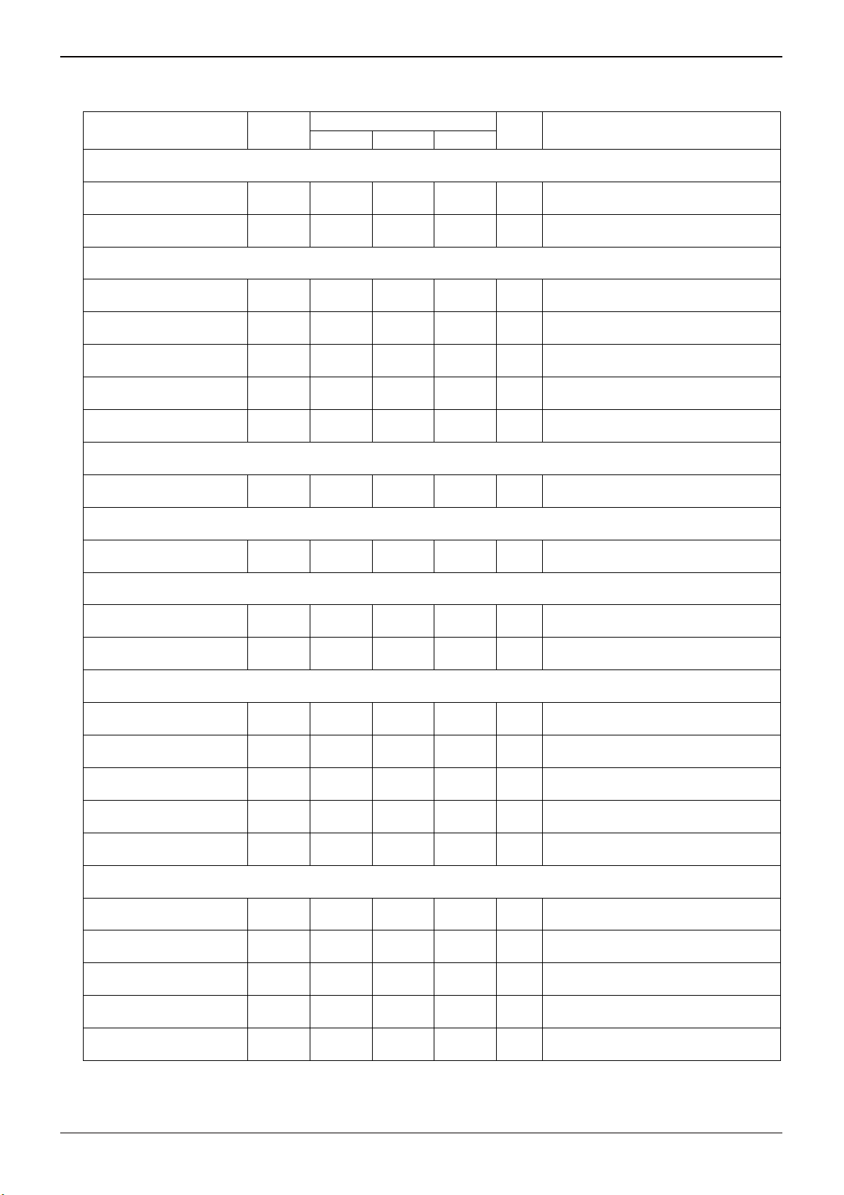
1) BD6757KN Electrical Characteristics (Unless otherwise specified, Ta=25°C, VCC=3.0V, VM=5.0V)
Parameter Symbol
Min. Typ. Max.
Limit
Unit Conditions
Overall
Technical Note
Circuit current
during standby operation
ICCST - 0 10 μA PS=0V
Circuit current ICC - 1.0 3.0 mA PS=VCC with no signal
Control input (IN=PS, IN1A to IN7B, and LIMSW)
High level input voltage VINH 2.0 - - V
Low level input voltage VINL - - 0.7 V
High level input current IINH 15 30 60 μA VINH=3V
Low level input current IINL -1 0 - μA VINL=0V
Pull-down resistor RIN 50 100 200 kΩ
Charge pump
Charge pump voltage VCP 10 11 - V
UVLO
UVLO voltage VUVLO 1.6 - 2.4 V
Full-ON Drive block (ch1 to ch6)
Output ON-Resistance RON - 1.3 1.6 Ω
Io=±400mA on high and low sides
in total
Pulse input response tp 100 - - ns With an input pulse with of 200ns
Linear Constant-Current Drive block (ch7)
Output ON-Resistance RON - 0.9 1.1 Ω
Io=±400mA on high and low sides
in total
VREF output voltage VREF 0.88 0.90 0.92 V Iout=0~1mA
Output limit current 1 IOL1 388 400 412 mA
Output limit current 2 IOL2 285 300 315 mA
Output limit current 3 IOL3 190 200 210 mA
RNF=0.5Ω with a load of 10Ω
VLIMH(L)=0.2V, LIMSW=0V(3V)
RNF=0.5Ω with a load of 10Ω
VLIMH(L)=0.15V, LIMSW=0V(3V)
RNF=0.5Ω with a load of 10Ω
VLIMH(L)=0.1V, LIMSW=0V(3V)
Digital NPN transistor block for photo-interrupter waveform shaping
Input current ISIH - - 0.1 mA SIx=3V
Low level output voltage VSOL - 0.1 0.25 V SIx=3V, ISO=0.5mA
Input dividing resistance RSIL 70 100 130 kΩ
Output pull-up resistance RSOH 5 10 20 kΩ
5
※
5
※
Input dividing resistance
comparison
※5 Design target value (Not all shipped devices are fully tested.)
www.rohm.com
© 2009 ROHM Co., Ltd. All rights reserved.
- 0.8 1.0 1.2 -
2/15
Division resistance comparison
between SIx and GND
5
※
2009.06 - Rev.A
BD6757KN, BD6889GU
Technical Note
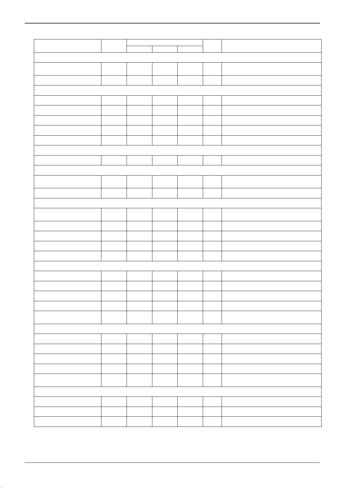
2) BD6889GU Electrical Characteristics (Unless otherwise specified, Ta=25°C, VCC=3.0V, VM=5.0V)
Parameter Symbol
Min. Typ. Max.
Limit
Unit Conditions
Overall
Circuit current
during standby operation
ICCST - 0 10 μA PS=0V
Circuit current ICC - 1.5 3.0 mA PS=VCC with no signal
Control input (IN=PS, IN1A to IN7B, SW, DSW, DSEL1, and DSEL2)
High level input voltage VINH 2.0 - - V
Low level input voltage VINL - - 0.7 V
High level input current IINH 15 30 60 μA VINH=3V
Low level input current IINL -1 0 - μA VINL=0V
Pull-down resistor RIN 50 100 200 kΩ
UVLO
UVLO voltage VUVLO 1.6 - 2.4 V
Full-ON Drive block (ch1 to ch6)
Output ON-Resistance RON - 1.3 1.6 Ω
Io=±400mA on high and low sides
in total
Pulse input response tp 100 - - ns With an input pulse with of 200ns
Linear Constant-Current Drive block (ch7)
Output ON-Resistance RON - 0.9 1.1 Ω
Io=±400mA on high and low sides
in total
VREF output voltage VREF 0.88 0.90 0.92 V Iout=0~1mA
Output limit current 1 IOL1 388 400 412 mA RNF=0.5Ω with a load of 10Ω, VLIM=0.2V
Output limit current 2 IOL2 285 300 315 mA RNF=0.5Ω with a load of 10Ω, VLIM=0.15V
Output limit current 3 IOL3 190 200 210 mA RNF=0.5Ω with a load of 10Ω, VLIM=0.1V
Digital NPN transistor block for photo-interrupter waveform shaping
Input current ISIH - - 0.1 mA SIx=3V
Low level output voltage VSOL - 0.1 0.25 V SIx=3V, ISO=0.5mA
Input dividing resistance RSIN 70 100 130 kΩ
Output pull-up resistance RSOH 23 33 43 kΩ
Input dividing resistance
comparison
- 0.8 1.0 1.2 -
Division resistance comparison
between SIx and GND
6
※
Digital PNP transistor block for photo-interrupter waveform shaping
Input current ISIL -0.1 - - mA SIx=0V
High level output voltage VSOH VCC-0.25 VCC-0.1 - V SIx=0V, ISO=-0.5mA
Input dividing resistance RSIP 70 100 130 kΩ
Output pull-down resistance RSOL 23 33 43 kΩ
Input dividing resistance
comparison
- 0.8 1.0 1.2 -
Division resistance comparison
between SIx and VCC
6
※
Voltage-regulator for photo-interrupter
High level output voltage VREGH VCC-0.25 VCC-0.2 - V IREG=100mA
Output ON-Resistance RONREG - 2 2.5 Ω IREG=100mA
Output leak current ILPI - 0 1 μA SW=VCC
※6 Design target value (Not all shipped devices are fully tested.)
www.rohm.com
© 2009 ROHM Co., Ltd. All rights reserved.
3/15
2009.06 - Rev.A
BD6757KN, BD6889GU
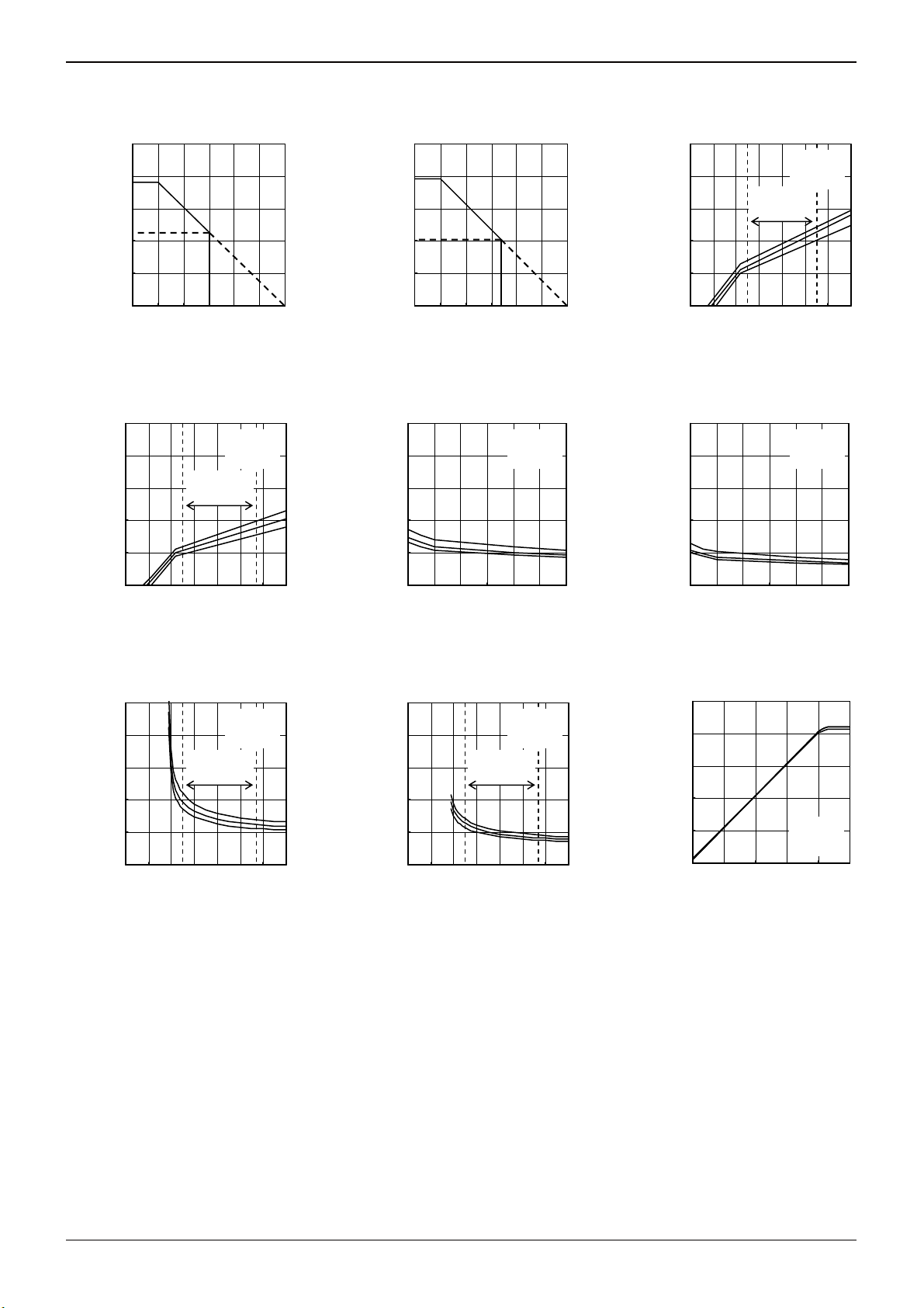
●Electrical Characteristic Diagrams
1250
1000
940mW
750
570mW
500
250
Power dissipation : Pd [mW]
0
0 25 50 75 100 125 150
Ambient t emperature : Ta [° C]
Fig.1 Power Dissipation Reduction
5.0
4.0
3.0
2.0
1.0
Circuit current : ICC [mA]
0.0
0.0 1.0 2.0 3.0 4.0 5.0 6.0 7.0
Fig.4 Circuit current
(2.5V to 5.7V)
Supply voltag e : VCC [V]
5.0
4.0
3.0
2.0
1.0
Output ON resistance : RON [Ω]
0.0
0.0 1.0 2.0 3.0 4.0 5.0 6.0 7.0
Fig.7 Output ON-Resistance
(Full-ON Drive block)
(2.5V to 5.7V)
Supply voltag e : VM [V]
75°C
Op. range
Op. range
BD6757KN
BD6889GU
Top 8 5 ° C
Mid 25°C
Low -25°C
BD6889GU
Top 8 5 ° C
Mid 25°C
Low -25°C
1250
980mW
1000
750
510mW
500
250
Power dissipation : Pd [mW]
0
0 25 50 75 100 125 150
Ambient t emperature : Ta [° C]
BD6889GU
85°C
Fig.2 Power Dissipation Reduction
5.0
4.0
3.0
2.0
1.0
Output ON resistance : RON [Ω]
0.0
9.0 10.0 11.0 12.0 13.0 14. 0 15. 0
Supply voltag e : VG [V]
BD6757KN
Top 7 5 ° C
Mid 25°C
Low -25°C
Fig.5 Output ON-Resistance
(Full-ON Drive block)
Op. range
BD6889GU
Top 8 5 ° C
Mid 25°C
Low -25°C
5.0
4.0
3.0
2.0
1.0
Output ON resistance : RON [Ω]
0.0
0.0 1.0 2.0 3.0 4.0 5.0 6.0 7.0
(2.5V to 5.7V)
Supply voltag e : VM [V]
Fig.8 Output ON-Resistance
(Linear Constant-Current Drive block)
5.0
4.0
3.0
2.0
1.0
Circuit current : ICC [mA]
0.0
5.0
4.0
3.0
2.0
1.0
Output ON resistance : RON [Ω]
0.0
(Linear Constant-Current Drive block)
250
200
150
100
RNF voltage : VRNF [mV]
Technical Note
BD6757KN
Top 7 5 ° C
Mid 25°C
Low -25°C
Op. range
(2.5V to 5.5V)
0.0 1.0 2.0 3.0 4.0 5.0 6.0 7.0
Supply voltag e : VCC [V]
Fig.3 Circuit current
BD6757KN
Top 7 5 ° C
Mid 25°C
Low -25°C
9.0 10.0 11.0 12. 0 13. 0 14.0 15.0
Supply voltag e : VG [V]
Fig.6 Output ON-Resistance
BD6757KN, BD6889GU
50
0
0 50 100 150 200 250
VLIM voltage : VLIM [mV]
Fig.9 Output limit voltage
(RNF=0.5Ω)
Top 8 5 ° C
Mid 25°C
Low -25°C
www.rohm.com
© 2009 ROHM Co., Ltd. All rights reserved.
4/15
2009.06 - Rev.A
BD6757KN, BD6889GU
Technical Note
●Pin arrangement and Pin Function
39
VG
CP4
CP3
CP2
CP1
VM3
IN4B
IN4A
SI1
SI2
OUT5A
OUT5B
PGND2
OUT6A
OUT6B
OUT7A
RNF
OUT7B
SENSE
SO2
SO1
52
IN3B
BD6757KN
IN7B
VM4
IN7A
GND
VREF
VLIMH
VM2
IN3A
IN2B
IN2A
IN1B
26
IN1A
OUT4A
OUT4B
OUT3A
OUT3B
PGND1
OUT2B
OUT2A
OUT1B
OUT1A
IN5A
IN5B
VLIML
LIMSW
VCC
VM1
PS
IN6B
IN6A
13
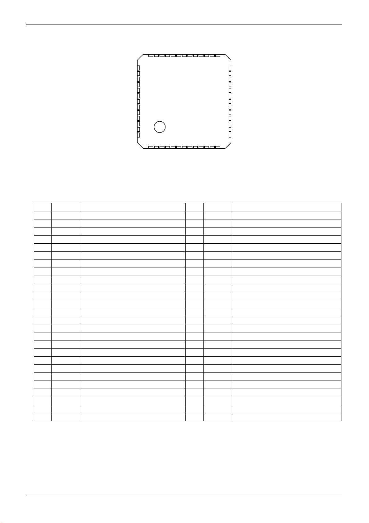
Fig.10 BD6757KN Pin Arrangement (Top View)
UQFN52 Package
BD6757KN Pin Function Table
No. Pin Name Function No. Pin Name Function
1 IN7B Control input pin ch7 B 27 IN2A Control input pin ch2 A
2 VM4 Motor power supply pin ch7 28 IN2B Control input pin ch2 B
3 IN7A Control input pin ch7 A 29 IN3A Control input pin ch3 A
4 GND Ground Pin 30 VM2 Motor power supply pin ch3 and ch4
5 VREF Reference voltage output pin 31 CP1 Charge pump capacitor connection pin 1
6 VLIMH Output current setting pin 1 ch7 32 CP2 Charge pump capacitor connection pin 2
7 VLIML Output current setting pin 2 ch7 33 CP3 Charge pump capacitor connection pin 3
8 LIMSW Output current setting selection pin ch7 34 CP4 Charge pump capacitor connection pin 4
9 VCC Power supply pin 35 VG Charge pump output pin
10 VM1 Motor power supply pin ch1 and ch2 36 VM3 Motor power supply pin ch5 and ch6
11 PS Power-saving pin 37 IN3B Control input pin ch3 B
12 IN6B Control input pin ch6 B 38 IN4A Control input pin ch4 A
13 IN6A Control input pin ch6 A 39 IN4B Control input pin ch4 B
14 IN5B Control input pin ch5 B 40 SI1 Digital transistor input pin 1
15 IN5A Control input pin ch5 A 41 SI2 Digital transistor input pin 2
16 OUT1A H-bridge output pin ch1 A 42 OUT5A H-bridge output pin ch5 A
17 OUT1B H-bridge output pin ch1 B 43 OUT5B H-bridge output pin ch5 B
18 OUT2A H-bridge output pin ch2 A 44 PGND2 Motor ground pin ch5 and ch6
19 OUT2B H-bridge output pin ch2 B 45 OUT6A H-bridge output pin ch6 A
20 PGND1 Motor ground pin ch1 to ch4 46 OUT6B H-bridge output pin ch6 B
21 OUT3B H-bridge output pin ch3 B 47 OUT7A H-bridge output pin ch7 A
22 OUT3A H-bridge output pin ch3 A 48 RNF Resistance connection pin for output current detection ch7
23 OUT4B H-bridge output pin ch4 B 49 OUT7B H-bridge output pin ch7 B
24 OUT4A H-bridge output pin ch4 A 50 SENSE Output current detection pin ch7
25 IN1A Control input pin ch1 A 51 SO2 Digital transistor output pin 2
26 IN1B Control input pin ch1 B 52 SO1 Digital transistor output pin 1
www.rohm.com
© 2009 ROHM Co., Ltd. All rights reserved.
5/15
2009.06 - Rev.A
 Loading...