1/4
STRUCTURE Silicon Monolithic Integrated Circuit
PRODUCT SERIES 1ch. Reversible Motor Driver
TYPE BD6736FV
FEATURES ・Full-ON type 1ch. H-bridge Driver
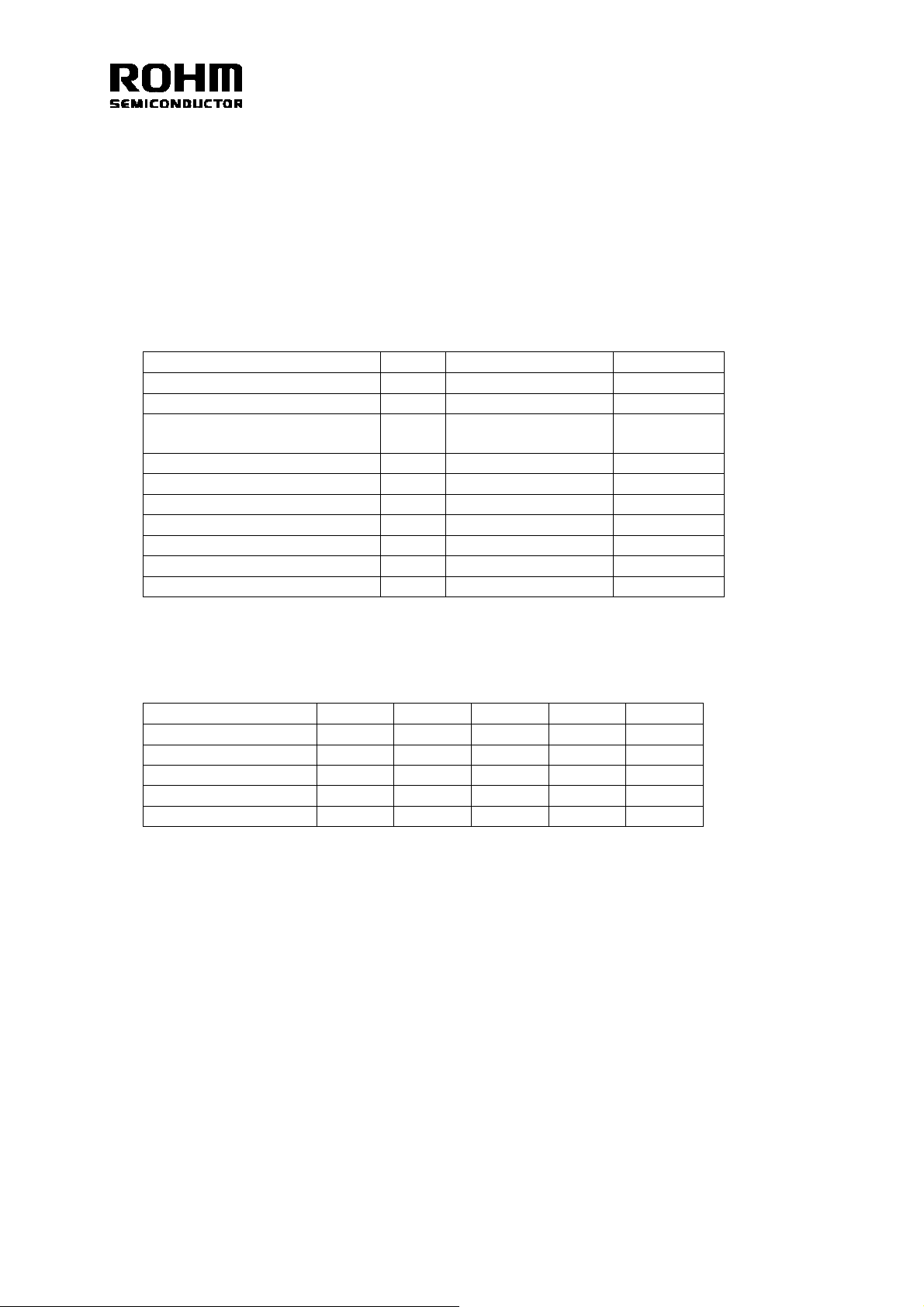
zAbsolute maximum ratings (Ta=25°C)
Parameter Symbol Limit Unit
Power supply voltage VCC -0.5 to +10.0 V
Motor power supply voltage VM -0.5 to +10.0 V
Charge pump step-up
power supply voltage
Control input voltage VIN -0.5 to VCC+0.5 V
Power dissipation Pd 930※1 mW
Operating temperature range Topr -30 to +75 °C
Junction temperature Tjmax 150 °C
Storage temperature range Tstg -55 to +150 °C
H-bridge output current DC Iout -1000 to +1000※2 mA
H-bridge output current (100msec) Iopeak -3200 to +3200※2 mA
※1
Reduced by 7.44mW/°C over 25°C, when mounted on a glass epoxy board (70mm × 70mm × 1.6mm)
※2
Must not exceed Pd, ASO, or Tjmax of 150°C.
VBST -0.5 to +15.0 V
zOperating Conditions (Ta= -30°C to +75°C)
Parameter Symbol Min. Typ. Max. Unit
Power supply voltage VCC 2.0 5.0 9.0 V
Motor power supply voltage VM 2.0 5.0 9.0 V
Control input voltage VIN 0 - VCC V
Logic input frequency FIN 0 - 100 kHz
Min. logic pulse width TIN 0.5 - - μs
The product described in this specification is a strategic product (and/or service) subject to COCOM regulations.
It should not be exported without authorization from the appropriate government authorities.
This product isn’t designed for protection against radioactive rays.
Status of this document: The Japanese version of this document is the formal specification. A customer may use this translation
version only for a reference to help reading the formal version. If there are any differences in translation version of this document,
formal version takes priority.
REV. C

2/4
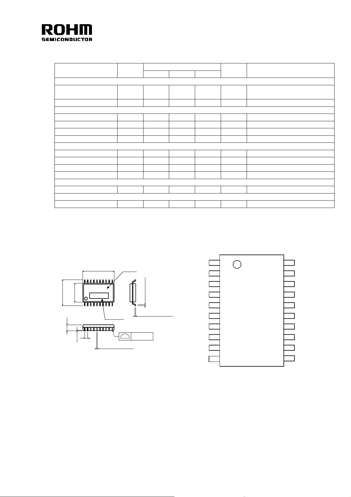
zBD6736FV Electrical Characteristics (Unless otherwise specified Ta=25°C, VCC=5.0V, VM=5.0V)
Parameter Symbol
Overall
Circuit current
during standby operation
Circuit current ICC 0.5 2.0 4.0 mA PS=H, FIN=100kHz
Power saving
High-level input voltage VPSH 2.0 - VCC V
Low-level input voltage VPSL -0.3 - 0.5 V
High-level input current IPSH 25 50 100 μA VPSH=5V
Low-level input current IPSL -1 0 1 μA VPSL=0V
Control input
High-level input voltage VINH 2.0 - VCC V
Low-level input voltage VINL -0.3 - 0.7 V
High-level input current IINH 25 50 100 μA VINH=5V
Low-level input current IINL -1 0 1 μA VINL=0V
UVLO
UVLO voltage VUVLO 1.5 - 1.9 V
Full-ON Drive block
Output ON-Resistance RON - 0.35 0.5 Ω Io=±500mA on high and low sides in total
ICCST - 0 1 μA PS=0V
Min. Typ. Max.
Limit
Unit Conditions
zPackage Outline zPin Arrangement (Top View)
1
6.4 ± 0.3
6.5 ± 0.2
20
4.4 ± 0.2
1
BD6736
11
10
Lot No.
Type name
0.3Min.
0.15 ± 0.1
1.15 ± 0.1
0.1
0.65
0.22 ± 0.1
0.1
VM
2
N.C.
3
OUTA
4
OUTA
MGND
5
MGND
6
OUTB
7
OUTB
8
VM
9
10
GND
Fig.1 SSOP-B20 Package (Unit: mm)
Fig.2 BD6736FV Pin Arrangement (Top View)
VCC
PS
INA
INB
PWM
CPL1
CPL2
CPH1
CPH2
BST
20
19
18
17
16
15
14
13
12
11
REV. C
 Loading...