

Page 1
System Lens Driver Series for Digital Still Cameras / Single-lens Reflex Cameras
1 to 2ch Lens Drivers
for Single-Lens Reflex Cameras
BD6735FV, BD6736FV
No.09014EAT03
●Description
The BD6735FV motor driver provides 2 Full-ON Drive H-bridge channels, while BD6736FV provides 1 Full-ON Drive H-bridge
channel. ROHM’s lens driver series features high voltage resistance and large current output in a compact surface mount
package, making it ideally suited for smaller systems such as Single-Lens Reflex with Interchangeable Lenses.
●Features
1) Low ON-Resistance Power MOS output: Full-ON Drive block with 1.0Ω Typ. (BD6735FV)
Full-ON Drive block with 0.35Ω Typ. (BD6736FV)
2) DMOS output allowing a range power supply: 2.0V to 8.0V (BD6735FV), 2.0V to 9.0V (BD6736FV)
3) Built-in step-up circuit for the DMOS gate voltage drive
4) Drive mode switching function
5) H bridge maximum output current: DC maximum 1.0A (BD6735FV and BD6736FV), Peak maximum 3.2A (BD6736FV)
6) UVLO (Under Voltage Lockout Protection) function
7) Built-in TSD (Thermal Shut Down) circuit
8) Standby current consumption: 0μA Typ.
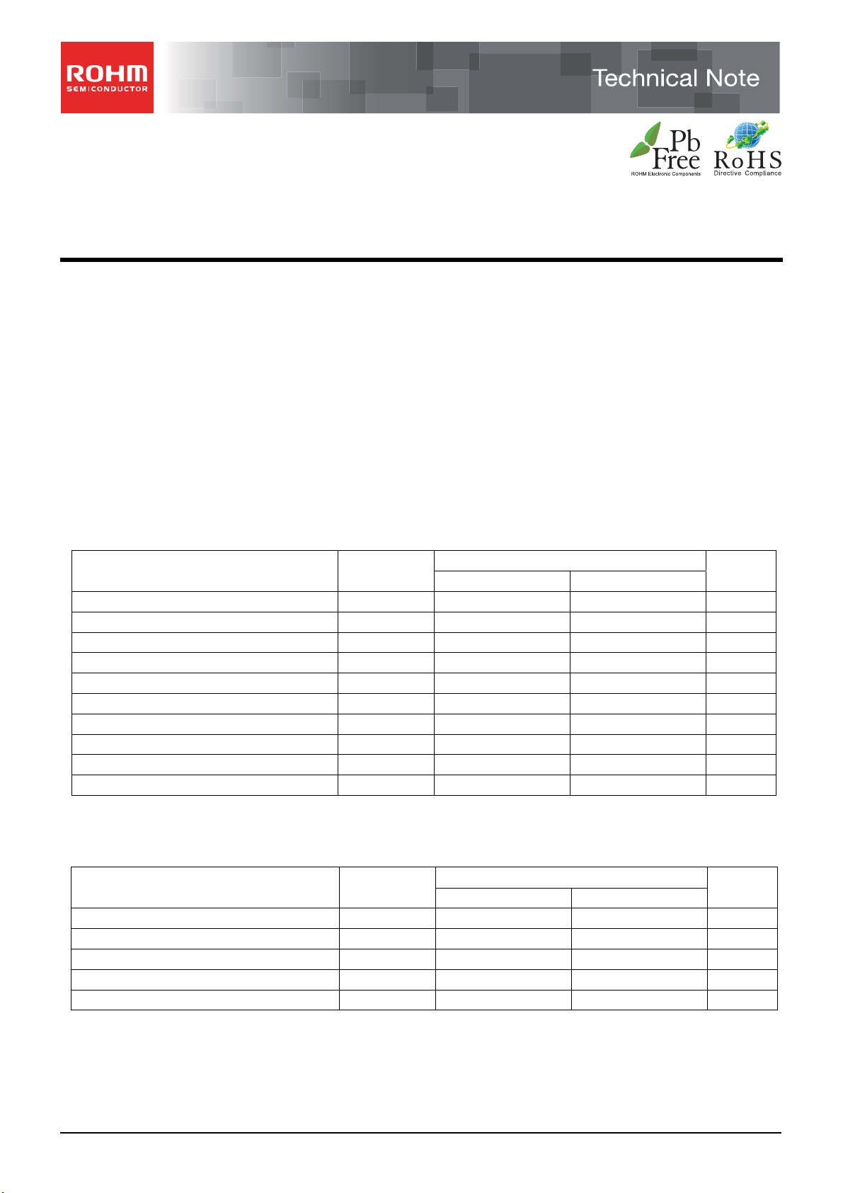
●Absolute Maximum Ratings
Parameter Symbol
BD6735FV BD6736FV
Limit
Unit
Power supply voltage VCC -0.5 to +10.0 -0.5 to +10.0 V
Motor power supply voltage VM -0.5 to +10.0 -0.5 to +10.0 V
Charge pump step-up power supply voltage VBST -0.5 to +15.0 -0.5 to +15.0 V
Control input voltage VIN -0.5 to VCC+0.5 -0.5 to VCC+0.5 V
Power dissipation Pd 810
1
※
810
1
※
mW
Operating temperature range Topr -30 to +75 -30 to +75 ℃
Junction temperature Tjmax +150 +150 ℃
Storage temperature range Tstg -55 to +150 -55 to +150 ℃
2
H-bridge output current (DC) Iout -1000 to +1000
※
-1000 to +1000
H-bridge output current (Peak) Ipeak - -3200 to +3200
※1 Reduced by 6.48mW/°C over 25℃, when mounted on a glass epoxy board (70mm 70mm 1.6mm).
※2 Must not exceed Pd, ASO, or Tjmax of 150℃
※3 Peak=100msec
2
※
mA/ch
3
※
mA/ch
●Operating Conditions (Ta=-30 to +75℃)
Parameter Symbol
BD6735FV BD6736FV
Limit
Power supply voltage VCC 2.0 to 8.0 2.0 to 9.0 V
Motor power supply voltage VM 2.0 to 8.0 2.0 to 9.0 V
Control input voltage VIN 0 to VCC 0 to VCC V
Logic input frequency FIN 0 to 100 0 to 100 kHz
Min. logic input pulse width TIN 0.5 0.5 μs
Unit
www.rohm.com
© 2009 ROHM Co., Ltd. All rights reserved.
1/8
2009.06 - Rev.A
Page 2
BD6735FV, BD6736FV
Technical Note
●Electrical Characteristics
1) BD6735FV and BD6736FV Electrical Characteristics (Unless otherwise specified, Ta=25°C, VCC=5.0V, VM=5.0V)
Parameter Symbol
Min. Typ. Max.
Limit
Unit Conditions
Overall
Circuit current
during standby operation
ICCST - 0 1 μA PS=0V
Circuit current (BD6735FV) ICC 0.5 2.0 4.0 mA PS=H, FIN=100kHz
Circuit current (BD6736FV) ICC 0.5 1.5 4.0 mA PS=H, FIN=100kHz
Power saving (PS)
High-level input voltage VPSH 2.0 - VCC V
Low-level input voltage VPSL -0.3 - 0.5 V
High-level input current IPSH 25 50 100 μA VPSH=5V
Low-level input current IPSL -1 0 1 μA VPSL=0V
Control input (BD6735FV; INxA, INxB, PWMEN, and BD6736FV; INA, INB, PWM)
High-level input voltage VINH 2.0 - VCC V
Low-level input voltage VINL -0.3 - 0.7 V
High-level input current IINH 25 50 100 μA VINH=5V
Low-level input current IINL -1 0 1 μA VINL=0V
UVLO
UVLO voltage VUVLO 1.5 - 1.9 V
BD6735FV Full-ON Drive block (ch1 and ch2)
Output ON-Resistance RON - 1.0 1.35 Ω Io=700mA on high and low sides in total
BD6736FV Full-ON Drive block (ch1)
Output ON-Resistance RON - 0.35 0.5 Ω Io=500mA on high and low sides in total
●Electrical Characteristics
1000
800
810mW
BD6735FV, BD6736FV
600
486mW
400
200
Power dissipation : Pd [mW]
0
0 25 50 75 100 125 150
Ambient temperature : Ta [°C]
75°C
Fig.1 Power Dissipation Reduction
800
600
BD6735FV
Top 7 5° C
Mid 25°C
Low -30°C
400
: VDSL [mV]
DS
200
Output V
0
0 200 400 600 800 1000
Output current : I
OUT
[mA]
Fig.4 Output ON-Voltage on Low-Side
5.0
4.0
3.0
2.0
1.0
Circuit current : ICC [mA]
0.0
0.0 2.0 4.0 6. 0 8.0 10.0
Fig.2 Circuit current
250
200
150
: VDSH [mV]
DS
100
50
Output V
0
0 200 400 600 800 1000
Fig.5 Output ON-Voltage on High-Side
BD6735FV, BD6736FV
BD6736FV Op. range
(2.0V to 9.0V)
BD6735FV Op. range
(2.0V to 8.0V)
Top 7 5° C
Mid 25°C
Low -30°C
Supply voltag e : VCC [V]
Top 7 5° C
Mid 25°C
Low -30°C
Output current : I
OUT
BD6736FV
[mA]
800
600
400
: VDSL [mV]
DS
200
Output V
0
0 200 400 600 800 1000
Output current : I
Fig.3 Output ON-Voltage on High-Side
250
200
150
: VDSH [mV]
DS
100
50
Output V
0
0 200 400 600 800 1000
Output current : I
Fig.6 Output ON-Voltage on Low-Side
BD6735FV
Top 7 5° C
Mid 25°C
Low -30°C
[mA]
OUT
BD6736FV
Top 7 5° C
Mid 25°C
Low -30°C
[mA]
OUT
www.rohm.com
© 2009 ROHM Co., Ltd. All rights reserved.
2/8
2009.06 - Rev.A
Page 3
BD6735FV, BD6736FV
●Application Circuit Diagram, Pin Function, and Pin Arrangement
Bypass filter Capacitor for
power supply input. (p.7/8)
Power-saving (p.5/8)
H : Active
L : Standby
Motor control input
(p.5/8)
Drive mode selection
(p.5/8)
H : EN/IN
L : IN/IN
PS
IN1A
IN1B
IN2A
IN2B
PWME N
20
19
18
17
16
15
Power Save
Logic
Power Save
OSC Charge Pump Charge Pump
10
GND
Connecting capacitors between the CPL1 and C PL2, CPH1 and CPH2, and BST and GND pins generate a
BST voltage. Use caution to ensure that the vo ltage differential between BST and VM is 3.0V or higher, and that
the BST voltage does not exceed the absolute maximum rating of 15V, especially set the BST voltage direct
input.(p.5/8)
Fig.7 BD6735FV Application Circuit Diagram
1~100uF
Level Shift
Pre Driver
14 12 9
CPL1 CPL2
0.1μF 0.1μF 1.0μF
VCC
1
BST
&
13
No. Pin Name Function
1 VCC Power supply pin
2 MGND2 Motor ground pin 2
3 OUT4 H-bridge output pin 4
4 OUT3 H-bridge output pin 3
5 VM Motor power supply pin
6 OUT1 H-bridge output pin 1
7 OUT2 H-bridge output pin 2
8 MGND1 Motor ground pin 1
9 BST Charge pump step-up power supply pin
10 GND Ground pin
11 CPH2 Capacitor connection pin for second charge 2
12 CPH1 Capacitor connection pin for second charge 1
13 CPL2 Capacitor connection pin for first charge 2
14 CPL1 Capacitor connection pin for first charge 1
15 PWMEN Drive mode selection pin
16 IN2B Control input pin ch2 B
17 IN2A Control input pin ch2 A
18 IN1B Control input pin ch1 B
19 IN1A Control input pin ch1 A
20 PS Power-saving pin
Fig.8 BD6735FV Pin Arrangement (Top View)
BandGapTSD & UVLO
5
6
7
4
3
2
8
BST
CPH1
H bridge
Full ON
H bridge
Full ON
11
CPH2
BD6735FV Pin Function Table
1~100uF
VM
OUT1
OUT2
OUT3
OUT4
MGND2
MGND1
Technical Note
Bypass filter Capacitor for
power supply input. (p.7/8)
M
www.rohm.com
© 2009 ROHM Co., Ltd. All rights reserved.
3/8
2009.06 - Rev.A
Page 4

BD6735FV, BD6736FV
Power-saving (p.5/8)
H : Active
L : Standby
Motor control input
(p.5/8)
PS
19
18
Drive mode selection
(p.5/8)
H : EN/IN
L : IN/IN
INA
INB
PWM
17
16
Connecting capacitors between the CPL1 and C PL2, CPH1 and CPH2, and BST and GND pins generate a
BST voltage. Use caution to ensure that the vo ltage differential between BST and VM is 3.0V or higher, and that
the BST voltage does not exceed the absolute maximum rating of 15V, especially set the BST voltage direct
input. (p.5/8)
Fig.10 BD6736FV Pin Arrangement (Top View)
Bypass filter Capacitor for
power supply input. (p.7/8)
1~100uF
Power Save
Logic
Power Save
OSC Charge Pump Charge Pump
10
GND
Level Shift
Pre Driver
15 13 11
CPL1 CPL2
0.1μF 0.1μF 1.0μF
VCC
20
BandGapTSD & UVLO
BST
CPH1
H bridge
Full ON
12
CPH2
&
14
Fig.9 BD6736FV Application Circuit Diagram
BD6736FV Pin Function Table
No. Pin Name Function
1 VM Motor power supply pin
2 N.C. 3 OUTA H-bridge output pin A
4 OUTA H-bridge output pin A
5 MGND Motor ground pin
6 MGND Motor ground pin
7 OUTB H-bridge output pin B
8 OUTB H-bridge output pin B
9 VM Motor power supply pin
10 GND Ground pin
11 BST Charge pump step-up power supply pin
12 CPH2 Capacitor connection pin for second charge 2
13 CPH1 Capacitor connection pin for second charge 1
14 CPL2 Capacitor connection pin for first charge 2
15 CPL1 Capacitor connection pin for first charge 1
16 PWM Drive mode selection pin
17 INB Control input pin ch1 B
18 INA Control input pin ch1 A
19 PS Power-saving pin
20 VCC Power supply pin
BST
Technical Note
Bypass filter Capacitor for
power supply input. (p.7/8)
1~100uF
1
9
VM
3
4
OUTA
OUTB
7
8
MGND
5
6
www.rohm.com
© 2009 ROHM Co., Ltd. All rights reserved.
4/8
2009.06 - Rev.A
Page 5

BD6735FV, BD6736FV
●Function Explanation
1) Power-saving function
When Low-level voltage is applied to PS pin, the IC will be turned off internally and the circuit current will be 0μA (Typ.).
During operating mode, PS pin should be High-level. (See the Electrical Characteristics; p.2/8)
2) Motor Control input
(1) INxA and INxB pins (BD6735FV), INA and INB pins (BD6736FV)
These pins are used to program and control the motor drive modes. (See the Electrical Characteristics; p.2/8, and I/O
Truth Table; p.5/8)
(2) PWMEN pin (BD6735FV), PWM pin (BD6736FV)
When the High-level voltage is applied to the PWMEN pin (PWM pin), the I/O logic can be set to EN/IN mode.
However, when the Low-level voltage is applied, the I/O logic can be set to IN/IN mode. (See the Electrical
Characteristics; p.2/8, and I/O Truth Table; p.5/8)
3) H-bridge
The 2-channel H-bridges can be controlled independently. For this reason, it is possible to drive the H-bridges
simultaneously, as long as the package thermal tolerances are not exceeded.
The H-bridge output transistors consist of Power DMOS with the charge pump step-up power supply BST.
The total H-bridge ON-Resistance on the high and low sides varies with the BST voltages.
4) Charge pump
Each output H-bridge on the high and low sides consists of Nch DMOS. Therefore, the gate voltage BST should be
higher than the VM voltage to drive the Nch DMOS on the high side.
The BD6735FV and BD6736FV have a built-in charge pump circuit that generates BST voltage by connecting an external
capacitor, between CPL1 and CPL2, CPH1 and CPH2, BST and GND.
In order to ensure better performance, the voltage differential between BST and VM must be 3.0V or higher, and the BST
voltage must not exceed the absolute maximum rating of 15.0V.
●I/O Truth Table
BD6735FV I/O Truth Table
INPUT OUTPUT
Drive mode
PS
PWM
EN
IN1A/2A IN1B/2B OUT1/3 OUT2/4
L X L L Brake
EN/IN
H
H L H L CW
H H L H CCW
H
IN/IN L
L L Z Z Standby
H L H L CW
L H L H CCW
H H L L Brake
- L X X X Z Z Standby
L: Low, H: High, X: Don’t care, Z: High Impedance
At CW, current flows from OUT1(3) to OUT2(4). At CCW, current flows from OUT2(4) to OUT1(3).
BD6736FV I/O Truth Table
Drive mode
PS PWM INA INB OUTA OUTB
INPUT OUTPUT
L X L L Brake
EN/IN
H
H L H L CW
H H L H CCW
H
IN/IN L
L L Z Z Standby
H L H L CW
L H L H CCW
H H L L Brake
- L X X X Z Z Standby
L: Low, H: High, X: Don’t care, Z: High Impedance
At CW, current flows from OUTA to OUTB. At CCW, current flows from OUTB to OUTA.
Technical Note
Output mode
Output mode
www.rohm.com
© 2009 ROHM Co., Ltd. All rights reserved.
5/8
2009.06 - Rev.A
Page 6

BD6735FV, BD6736FV
Technical Note
●I/O Circuit Diagram
PS
VCC
100kΩ
INxA, INxB, PWMEN (BD6735FV)
INA, INB, PWM (BD6736FV)
VCC
10kΩ
VCC
70kΩ
VM, MGND, OUT1~4 (BD6735FV) VM, MGND, OUTA, B (BD6736FV)
VM
OUT1, 3
CPH1, CPL1
275kΩ
100kΩ
BST, CPH2, CPL2
3.33kΩ
OUT2, 4
VCC
MGND
VM Inside REG
BST
CPH2
CPL2
Fig.11 I/O Circuit Diagram (Resistance values are typical ones)
VM
●Notes for use
1) Absolute maximum ratings
Use of the IC in excess of absolute maximum ratings such as the applied voltage or operating temperature range may
result in IC damage. Assumptions should not be made regarding the state of the IC (short mode or open mode) when such
damage is suffered. The implementation of a physical safety measure such as a fuse should be considered when use of
the IC in a special mode where the absolute maximum ratings may be exceeded is anticipated.
2) Storage temperature range
As long as the IC is kept within this range, there should be no problems in the IC’s performance. Conversely, extreme
temperature changes may result in poor IC performance, even if the changes are within the above range.
3) Power supply pins and lines
None of the VM line for the H-bridges is internally connected to the VCC power supply line, which is only for the control
logic or analog circuit. Therefore, the VM and VCC lines can be driven at different voltages. Although these lines can be
connected to a common power supply, do not open the power supply pin but connect it to the power supply externally.
Regenerated current may flow as a result of the motor's back electromotive force. Insert capacitors between the power
supply and ground pins to serve as a route for regenerated current. Determine the capacitance in full consideration of all
the characteristics of the electrolytic capacitor, because the electrolytic capacitor may loose some capacitance at low
temperatures. If the connected power supply does not have sufficient current absorption capacity, regenerative current will
cause the voltage on the power supply line to rise, which combined with the product and its peripheral circuitry may exceed
the absolute maximum ratings. It is recommended to implement a physical safety measure such as the insertion of a
voltage clamp diode between the power supply and ground pins.
For this IC with 2 power supplies and a part consists of the CMOS block, it is possible that rush current may flow
instantaneously due to the internal powering sequence and delays, and to the unstable internal logic, respectively. Therefore,
give special consideration to power coupling capacitance, width of power and ground wirings, and routing of wiring.
4) Ground pins and lines
Ensure a minimum GND pin potential in all operating conditions. Make sure that no pins are at a voltage below the GND at
any time, regardless of whether it is a transient signal or not.
When using both small signal GND and large current MGND patterns, it is recommended to isolate the two ground patterns,
placing a single ground point at the application's reference point so that the pattern wiring resistance and voltage variations
caused by large currents do not cause variations in the small signal ground voltage. Be careful not to change the GND
wiring pattern of any external components, either.
The power supply and ground lines must be as short and thick as possible to reduce line impedance.
VM
VM
OUTA
OUTB
MGND
www.rohm.com
© 2009 ROHM Co., Ltd. All rights reserved.
6/8
2009.06 - Rev.A
Page 7

BD6735FV, BD6736FV
Technical Note
5) Thermal design
Use a thermal design that allows for a sufficient margin in light of the power dissipation (Pd) in actual operating conditions.
6) Pin short and wrong direction assembly of the device
Use caution when positioning the IC for mounting on printed circuit boards. The IC may be damaged if there is any
connection error or if positive and ground power supply terminals are reversed. The IC may also be damaged if pins are
shorted together or are shorted to other circuit’s power lines.
7) Actions in strong magnetic field
Use caution when using the IC in the presence of a strong magnetic field as doing so may cause the IC to malfunction.
8) ASO
When using the IC, set the output transistor for the motor so that it does not exceed absolute maximum ratings or ASO.
9) Thermal shutdown circuit
If the junction temperature (Tjmax) reaches 175°C (BD6735FV Typ.) and 160°C (BD6736FV Typ.), the TSD circuit will
operate, and the coil output circuit of the motor will open. There is a temperature hysteresis of approximately 20°C. The
TSD circuit is designed only to shut off the IC in order to prevent runaway thermal operation. It is not designed to protect
the IC or guarantee its operation. The performance of the IC’s characteristics is not guaranteed and it is recommended that
the device is replaced after the TSD is activated.
10) Testing on application board
When testing the IC on an application board, connecting a capacitor to a pin with low impedance subjects the IC to stress.
Always discharge capacitors after each process or step. Always turn the IC's power supply off before connecting it to, or
removing it from a jig or fixture, during the inspection process. Ground the IC during assembly steps as an antistatic
measure. Use similar precaution when transporting and storing the IC.
11) Application example
The application circuit is recommended for use. Make sure to confirm the adequacy of the characteristics. When using the
circuit with changes to the external circuit constants, make sure to leave an adequate margin for external components
including static and transitional characteristics as well as dispersion of the IC.
12) Regarding input pin of the IC
This monolithic IC contains P
+
isolation and P substrate layers between adjacent elements to keep them isolated. P-N
junctions are formed at the intersection of these P layers with the N layers of other elements, creating a parasitic diode or
transistor. For example, the relation between each potential is as follows:
When GND > Pin A, the P-N junction operates as a parasitic diode.
When GND > Pin B, the P-N junction operates as a parasitic diode and transistor.
Parasitic elements can occur inevitably in the structure of the IC. The operation of parasitic elements can result in mutual
interference among circuits, operational faults, or physical damage. Accordingly, methods by which parasitic elements
operate, such as applying a voltage that is lower than the GND (P substrate) voltage to an input pin, should not be used.
Pin A
N
P+ P
P
Parasitic element
GND
Resistor Transistor (NPN)
Pin A
+
N N
P substrate
Parasitic
element
Fig.12 Example of Simple IC Architecture
Pin B
C
N
Parasitic element
P+
B
E
N
P
P+
N
P substrate
GND
GND
Pin B
B C
Other adjacent
elements
E
GND
Parasitic
element
www.rohm.com
© 2009 ROHM Co., Ltd. All rights reserved.
7/8
2009.06 - Rev.A
Page 8

BD6735FV, BD6736FV
●Ordering part number
B D 6 7 3 5 F V - E 2
Technical Note
Part No. Part No.
6735 : 8.0V power supply voltage
6736 : 9.0V power supply voltage
3.2A peak current
SSOP-B20
6.5 ± 0.2
20
11
6.4 ± 0.3
4.4 ± 0.2
1
10
1.15 ± 0.1
0.1± 0.1
0.65
0.22 ± 0.1
Package
FV : SSOP-B20
<Tape and Reel information>
Embossed carrier tapeTape
Quantity
Direction
0.3Min.
0.15 ± 0.1
0.1
(Unit : mm)
of feed
2500pcs
E2
The direction is the 1pin of product is at the upper left when you hold
()
reel on the left hand and you pull out the tape on the right hand
Reel
Packaging and forming specification
E2: Embossed tape and reel
1pin
Order quantity needs to be multiple of the minimum quantity.
∗
Direction of feed
www.rohm.com
© 2009 ROHM Co., Ltd. All rights reserved.
8/8
2009.06 - Rev.A
Page 9

Notes
No copying or reproduction of this document, in part or in whole, is permitted without the
consent of ROHM Co.,Ltd.
The content specied herein is subject to change for improvement without notice.
The content specied herein is for the purpose of introducing ROHM's products (hereinafter
"Products"). If you wish to use any such Product, please be sure to refer to the specications,
which can be obtained from ROHM upon request.
Examples of application circuits, circuit constants and any other information contained herein
illustrate the standard usage and operations of the Products. The peripheral conditions must
be taken into account when designing circuits for mass production.
Great care was taken in ensuring the accuracy of the information specied in this document.
However, should you incur any damage arising from any inaccuracy or misprint of such
information, ROHM shall bear no responsibility for such damage.
The technical information specied herein is intended only to show the typical functions of and
examples of application circuits for the Products. ROHM does not grant you, explicitly or
implicitly, any license to use or exercise intellectual property or other rights held by ROHM and
other par ties. ROHM shall bear no responsibility whatsoever for any dispute arising from the
use of such technical information.
Notice
The Products specied in this document are intended to be used with general-use electronic
equipment or devices (such as audio visual equipment, ofce-automation equipment, communication devices, electronic appliances and amusement devices).
The Products specied in this document are not designed to be radiation tolerant.
While ROHM always makes efforts to enhance the quality and reliability of its Products, a
Product may fail or malfunction for a variety of reasons.
Please be sure to implement in your equipment using the Products safety measures to guard
against the possibility of physical injury, re or any other damage caused in the event of the
failure of any Product, such as derating, redundancy, re control and fail-safe designs. ROHM
shall bear no responsibility whatsoever for your use of any Product outside of the prescribed
scope or not in accordance with the instruction manual.
The Products are not designed or manufactured to be used with any equipment, device or
system which requires an extremely high level of reliability the failure or malfunction of which
may result in a direct threat to human life or create a risk of human injur y (such as a medical
instrument, transportation equipment, aerospace machinery, nuclear-reactor controller,
fuel-controller or other safety device). ROHM shall bear no responsibility in any way for use of
any of the Products for the above special purposes. If a Product is intended to be used for any
such special purpose, please contact a ROHM sales representative before purchasing.
If you intend to export or ship overseas any Product or technology specied herein that may
be controlled under the Foreign Exchange and the Foreign Trade Law, you will be required to
obtain a license or permit under the Law.
Thank you for your accessing to ROHM product informations.
More detail product informations and catalogs are available, please contact us.
ROHM Customer Support System
www.rohm.com
© 2009 ROHM Co., Ltd. All rights reserved.
http://www.rohm.com/contact/
R0039
A
 Loading...