

t
Datashee
DC Brushless Fan Motor Drivers
Multifunction Single-phase Full-wave
Fan Motor Driver
BD6721FS
●General description
BD6721FS is a 1chip driver that composes H-bridge of
power DMOS FET.
Moreover, because the level amplifier is installed, the
temperature control by the thermistor is also easy.
●Features
Driver including power DMOS FET
Speed controllable by DC / direct PWM input
PWM soft switching
Quick start
Current limit
Lock protection and automatic restart
Rotation speed pulse signal (FG) output
Lock alarm signal (AL) output
●Application
Fan motors for general consumer equipment of desktop PC, and Projector, etc.
●Absolute maximum ratings
Parameter Symbol Limit Unit
Supply voltage Vcc 20 V
Power dissipation Pd 812.5
Operating temperature range Topr –40 to +100 °C
Storage temperature range Tstg –55 to +150 °C
Output voltage Vo 20 V
Output current Io 1.0
Rotation speed pulse signal (FG) output voltage Vfg 20 V
Rotation speed pulse signal (FG) output current Ifg 10 mA
Lock alarm signal (AL) output voltage Val 20 V
Lock alarm signal (AL) output current Ial 10 mA
Reference voltage (REF) output current Iref 8 mA
Junction temperature Tj 150 °C
*1 Reduce by 6.5mW/°C over Ta=25°C. (On 70.0mm×70.0mm×1.6mm glass epoxy board)
*2 This value is not to exceed Pd.
●Recommended operating conditions
Parameter Symbol Limit Unit
Operating supply voltage range Vcc 4.5 to 17.0 V
Operating input voltage range
(H+, H–, TH, MIN, LAIN) (more than Vcc=9V)
Operating input voltage range
(H+, H–, TH, MIN, LAIN) (less than Vcc=9V)
●Package W (Typ.) x D (Typ.) x H (Max.)
SSOP-A16 6.60mm x 6.20mm x 1.71mm
*1
mW
*2
A
0 to 7 V
Vin
0 to Vcc–2 V
SSOP-A16
○Product structure:Silicon monolithic integrated circuit ○This product is not designed protection against radioactive rays
www.rohm.com
© 2012 ROHM Co., Ltd. All rights reserved.
TSZ22111・14・001
1/13
TSZ02201-0H1H0B100170-1-2
28.JUL.2012 Rev.002
Datasheet
BD6721FS
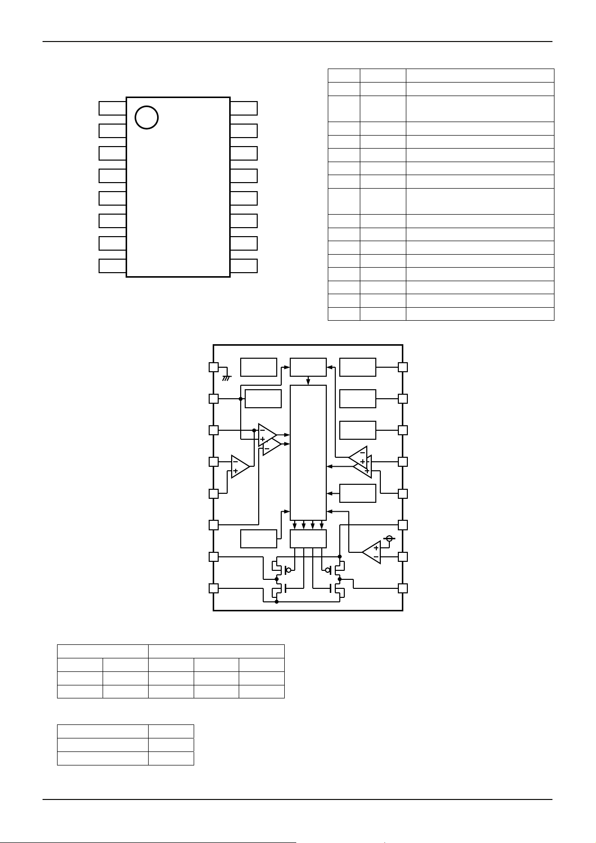
●Pin configuration
GND
OSC
1
2
LAOUT
LAIN
MIN
OUT1
RNF
TH
3
4
5
6
7
8
Fig.1 Pin configuration
●Block diagram
●I/O truth table
Hall input Driver output
H+ H– OUT1 OUT2 FG
H L L H Hi-Z
L H H L L
H; High, L; Low, Hi-Z; High impedance
FG output is open-drain type.
Motor state AL
Rotating L
Locking Hi-Z
L; Low, Hi-Z; High impedance
AL output is open-drain type.
(TOP VIEW)
Datasheet
●Pin description
P/No. T/Name Function
1 GND Ground terminal (signal ground)
16
15
AL
FG
2 OSC
3 LAOUT Level amplifier output terminal
Oscillating capacitor connecting
terminal
4 LAIN Level amplifier input terminal
REF
14
5 TH Output duty controllable input terminal
6 MIN Minimum output duty setting terminal
13
12
11
H–
H+
Vcc
7 OUT1 Motor output terminal 1
8 RNF
Output current detecting resistor
connecting terminal (motor ground)
9 OUT2 Motor output terminal 2
10 CS Output current detection terminal
CS
10
9
OUT2
11 Vcc Power supply terminal
12 H+ Hall + input terminal
13 H– Hall – input terminal
14 REF Reference voltage output terminal
15 FG Speed pulse signal output terminal
16 AL Lock alarm signal output terminal
Vcl
OUT2
AL
FG
REF
H–
H+
Vcc
CS
16
15
14
13
12
11
10
9
GND
1
OSC
2
LA
OUT
3
TSD
OSC
LA
IN
4
LEVEL
AMP
5
TH
MIN
6
QUICK
START
OUT1
7
RNF
8
PWM
COMP
PWM
COMP
PWM SOFT
SWITCHING
CONTROL
LOGIC
PRE-
DRIVER
SIGNAL
OUTPUT
SIGNAL
OUTPUT
REF
HALL
AMP
HALL
COMP
LOCK
PROTECT
CURRENT
LIMIT COMP
Fig.2 Block diagram
www.rohm.com
© 2012 ROHM Co., Ltd. All rights reserved.
TSZ22111・15・001
2/13
TSZ02201-0H1H0B100170-1-2
28.JUL.2012 Rev.002

Datasheet
BD6721FS
●Electrical characteristics(Unless otherwise specified Ta=25°C, Vcc=12V)
Parameter Symbol
Circuit current Icc 4 7 10 mA Fig.3
Hall input hysteresis voltage Vhys ±5 ±10 ±15 mV Fig.4
Output voltage Vo - 0.6 0.9 V
Lock detection ON time Ton 0.3 0.5 0.7 s Fig.9
Lock detection OFF time Toff 3.0 5.0 7.0 s Fig.10
FG output low voltage Vfgl - 0.15 0.30 V Ifg=5mA Fig.11, 12
FG output leak current Ifgl - - 10 µA Vfg=17V Fig.13
AL output low voltage Vall - 0.15 0.30 V Ial=5mA Fig.11, 12
AL output leak current Iall - - 10 µA Val=17V Fig.13
OSC high voltage Vosch 2.3 2.5 2.7 V Fig.14
OSC low voltage Voscl 0.8 1.0 1.2 V Fig.14
OSC charge current Icosc –50 –32 –26 µA Fig.15
OSC discharge current Idosc 26 32 50 µA Fig.15
Level amplifier gain Gla 50 - - dB Fig.16, 17
Level amplifier output high voltage Vlaoh - 1.6 2.0 V For Vcc voltage Fig.18
Level amplifier output low voltage Vlaol - 0.2 0.3 V Fig.19
Output ON duty 1 Poh1 85 90 95 %
Output ON duty 2 Poh2 45 50 55 %
Output ON duty 3 Poh3 5 10 15 %
Reference voltage Vref 2.8 3.0 3.2 V Iref=–2mA Fig.20, 21
Current limit setting voltage Vcl 290 310 330 mV Fig.22
TH input bias current Ith - - –0.2 µA Vth=0V Fig.23
MIN input bias current Imin - - –0.2 µA Vmin=0V Fig.24
About a current item, define the inflow current to IC as a positive notation, and the outflow current from IC as a negative notation.
Limit
Min. Typ. Max.
Unit Conditions
Io=±300mA,
High and low side total
Vth=Vref x 0.383
Output 1kΩ, OSC=470pF
Vth=Vref x 0.583
Output 1kΩ, OSC=470pF
Vth=Vref x 0.783
Output 1kΩ, OSC=470pF
Datasheet
Ref.
data
Fig.5 to 8
-
-
-
www.rohm.com
© 2012 ROHM Co., Ltd. All rights reserved.
TSZ22111・15・001
3/13
TSZ02201-0H1H0B100170-1-2
28.JUL.2012 Rev.002
Datasheet
BD6721FS
–
–
–
–
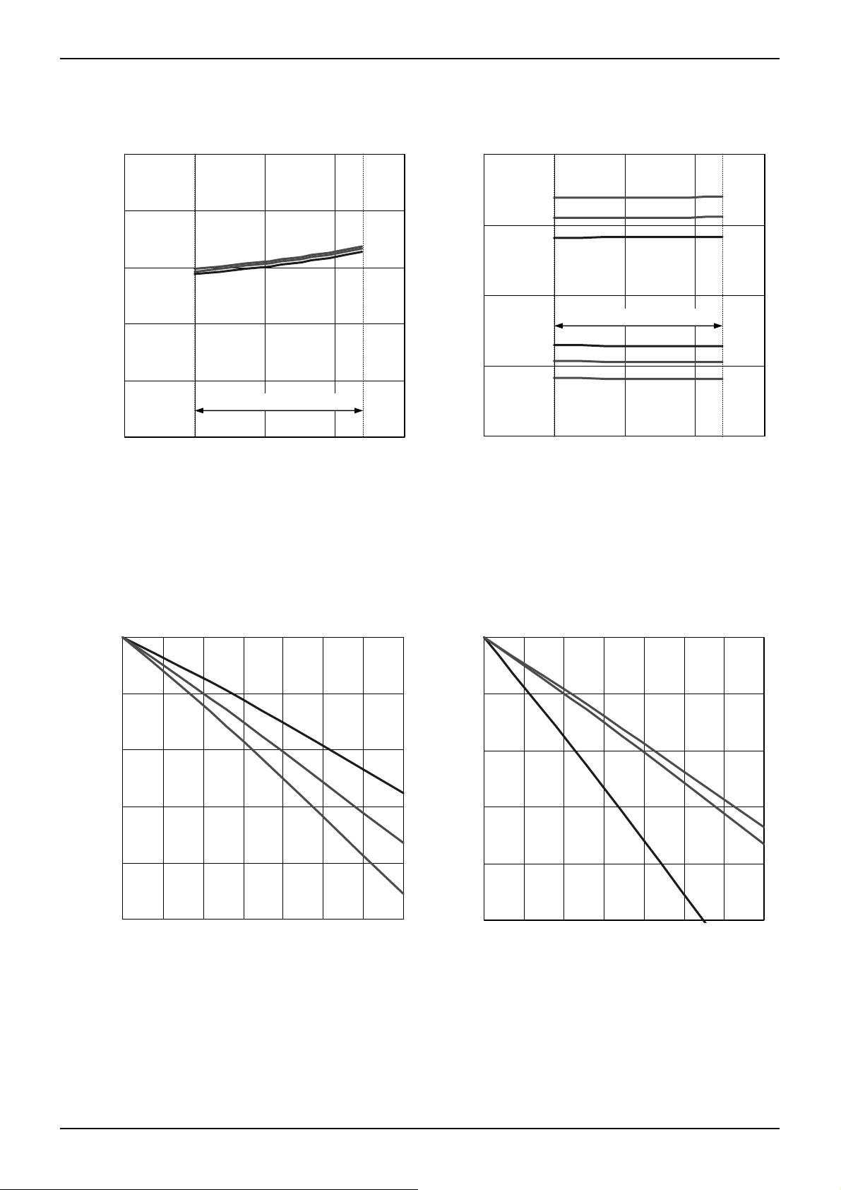
●Typical performance curves(Reference data)
10
8
6
4
Circuit current: Icc[mA]
2
Operating range
0
0 5 10 15 20
Supply voltage: Vcc[V]
Fig.3 Circuit current
0.0
-0.2
-0.4
-0.6
Output high voltage: Voh[V]
-0.8
-1.0
0.0 0.1 0.2 0.3 0.4 0.5 0.6 0.7
Output source current: Io[A]
Fig.5 Output high voltage (Vcc=12V)
25°C
100°C
40°C
40°C
25°C
100°C
20
10
0
Operating range
-10
Hall input hysteresis voltage: Vhys[mV]
-20
0 5 10 15 20
Supply voltage: Vcc[V]
Fig.4 Hall input hysteresis voltage
0.0
-0.2
-0.4
-0.6
Output high voltage: Voh[V]
-0.8
-1.0
0.0 0.1 0.2 0.3 0.4 0.5 0.6 0.7
Output source current: Io[A]
Fig.6 Output high voltage (Ta=25°C)
Datasheet
100°C
25°C
40°C
40°C
25°C
100°C
17V
12V
5V
www.rohm.com
© 2012 ROHM Co., Ltd. All rights reserved.
TSZ22111・15・001
4/13
TSZ02201-0H1H0B100170-1-2
28.JUL.2012 Rev.002
Datasheet
BD6721FS
–
–
–
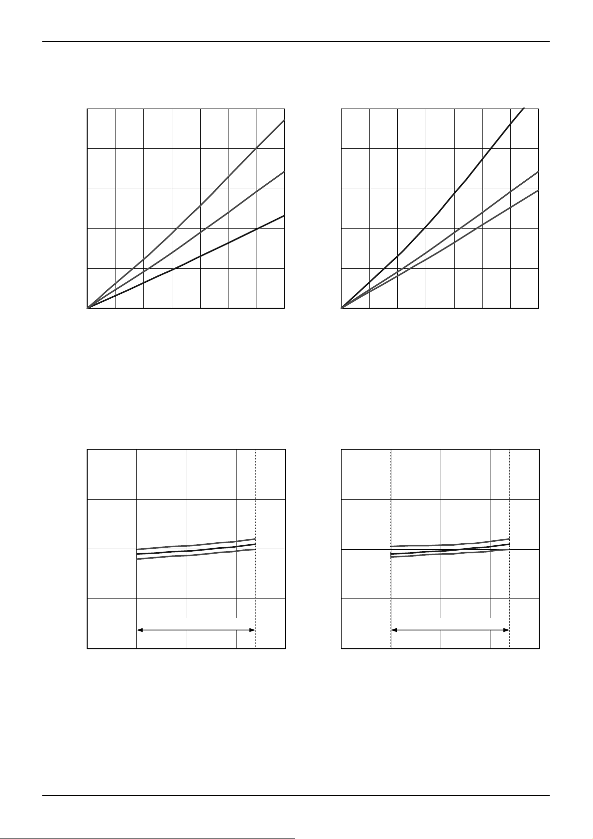
●Typical performance curves(Reference data)
1.0
0.8
0.6
0.4
Output low voltage: Vol[V]
0.2
0.0
0.0 0.1 0.2 0.3 0.4 0.5 0.6 0.7
Output sink current: Io[A]
Fig.7 Output low voltage (Vcc=12V)
0.7
0.6
0.5
0.4
Lock detection ON time: Ton[s]
Operating range
0.3
0 5 10 15 20
Supply voltage: Vcc[V]
Fig.9 Lock detection ON time
100°C
25°C
40°C
100°C
40°C
25°C
1.0
0.8
0.6
0.4
Output low voltage: Vol[V]
0.2
0.0
0.0 0.1 0.2 0.3 0.4 0.5 0.6 0.7
Output sink current: Io[A]
Fig.8 Output low voltage (Ta=25°C)
7.0
6.0
5.0
4.0
Lock detection OFF time: Toff[s]
Operating range
3.0
0 5 10 15 20
Supply voltage: Vcc[V]
Fig.10 Lock detection OFF time
Datasheet
5V
12V
17V
100°C
40°C
25°C
www.rohm.com
© 2012 ROHM Co., Ltd. All rights reserved.
TSZ22111・15・001
5/13
TSZ02201-0H1H0B100170-1-2
28.JUL.2012 Rev.002

Datasheet
BD6721FS
–
–
–
–
●Typical performance curves(Reference data)
0.8
0.6
0.4
0.2
FG/AL output low voltage: Vfgl /Vall[V]
0.0
0246810
Output sink current: Ifg/Ial[mA]
Fig.11 FG/AL output low voltage (Vcc=12V)
8
6
4
2
0
FG/AL output leak current: Ifgl/Iall[uA]
-2
0 5 10 15 20
Fig.13 FG/AL output leak current
Operating range
Supply voltage: Vcc[V]
100°C
25°C
40°C
100°C
25°C
40°C
Datasheet
0.8
0.6
0.4
0.2
FG/AL output low voltage: Vfgl /Vall[V]
0.0
0246810
Output sink current: Ifg/Ial[mA]
Fig.12 FG/AL output low voltage (Ta=25°C)
3.0
100°C
2.5
2.0
Operating range
1.5
100°C
1.0
OSC high/low voltage: Vosch/Voscl [V]
0.5
0 5 10 15 20
Supply voltage: Vcc[V]
Fig.14 OSC high/low voltage
5V
12V
17V
25°C
40°C
25°C
40°C
www.rohm.com
© 2012 ROHM Co., Ltd. All rights reserved.
TSZ22111・15・001
6/13
TSZ02201-0H1H0B100170-1-2
28.JUL.2012 Rev.002

Datasheet
BD6721FS
–
–
–
–
●Typical performance curves(Reference data)
60
40
20
0
-20
-40
OSC charge/discharge current: Icosc/Idosc [uA]
-60
0 5 10 15 20
Fig.15 OSC charge/discharge current
70
17V
12V
5V
60
50
40
Level amplifier gain: Gla[dB]
30
1.E+01 1.E+02 1.E+03 1.E+04
Fig.17 Level amplifier gain (Ta=25°C)
Operating range
Supply voltage: Vcc[V]
Input frequency: Flain[Hz]
40°C
25°C
100°C
100°C
25°C
40°C
Datasheet
70
60
50
40
Level amplifier gain: Gla[dB]
30
1.E+01 1.E+02 1.E+03 1.E+04
Input frequency: Flain[Hz]
Fig.16 Level amplifier gain (Vcc=12V)
2.0
1.8
1.6
1.4
1.2
Level amplifier output high voltage: Vlaoh[V]
1.0
0 5 10 15 20
Fig.18 Level amplifier output high voltage
Operating range
Supply voltage: Vcc[V]
40°C
25°C
100°C
40°C
25°C
100°C
www.rohm.com
© 2012 ROHM Co., Ltd. All rights reserved.
TSZ22111・15・001
7/13
TSZ02201-0H1H0B100170-1-2
28.JUL.2012 Rev.002

Datasheet
BD6721FS
–
–
–
–
●Typical performance curves(Reference data)
0.20
0.15
0.10
0.05
Level amplifi er output low voltage: Vlaol[V]
0.00
0 5 10 15 20
Fig.19 Level amplifier output low voltage
3.2
3.1
3.0
Reference voltage: Vref[V]
2.9
2.8
02468
Output source current: Iref[mA]
Fig.21 Reference voltage current ability (Vcc=12V)
Operating range
Supply voltage: Vcc[V]
100°C
25°C
40°C
100°C
25°C
40°C
3.2
3.1
3.0
Reference voltage: Vref[V]
2.9
Operating range
2.8
0 5 10 15 20
Supply voltage: Vcc[V]
Fig.20 Reference voltage
340
325
310
295
Current limit setting voltage: Vcl[mV]
280
0 5 10 15 20
Fig.22 Current limit setting voltage
Operating range
Supply voltage: Vcc[V]
Datasheet
100°C
25°C
40°C
100°C
25°C
40°C
www.rohm.com
© 2012 ROHM Co., Ltd. All rights reserved.
TSZ22111・15・001
8/13
TSZ02201-0H1H0B100170-1-2
28.JUL.2012 Rev.002

Datasheet
BD6721FS
–
–
●Typical performance curves(Reference data)
0.05
0.00
-0.05
-0.10
TH bias current: Ith[uA]
-0.15
-0.20
0 5 10 15 20
Operating range
Supply voltage: Vcc[V]
Fig.23 TH bias current
100°C
25°C
40°C
0.05
0.00
-0.05
-0.10
MIN bias current: Imin[uA]
-0.15
Operating range
-0.20
0 5 10 15 20
Supply voltage: Vcc[V]
Fig.24 MIN bias current
Datasheet
100°C
25°C
40°C
www.rohm.com
© 2012 ROHM Co., Ltd. All rights reserved.
TSZ22111・15・001
9/13
TSZ02201-0H1H0B100170-1-2
28.JUL.2012 Rev.002

Datasheet
BD6721FS
●Application circuit example(Constant values are for reference)
Output PWM frequency setting Hall bias is set according to the
Circuit that converts PWM duty
into DC voltage
to 1000pF
PWM
Minimum output duty setting
Maximum output voltage and
current are 20V and 1.0A.
To limit motor current, the
current is detected.
Note the power consumption of
detection resistance.
0.33Ω to
-
Gain setting according to
thermistor characteristic
Fig.25 PWM controllable 4 wires type (FG) motor application circuit
to 1000pF
Temperature control setting by
thermistor and linearized
resistance
330pF
330pF
1
2
3
4
5
6
7
8
1
2
3
4
5
GND
OSC
LA
OUT
LA
IN
TH
MIN
OUT1
RNF
GND
OSC
LA
OUT
LA
IN
TH
LEVEL
AMP
LEVEL
AMP
TSD
OSC
QUICK
START
PWM
COMP
PWM
COMP
PWM SOFT
SWITCHING
CONTROL
LOGIC
PRE-
DRIVER
SIGNAL
OUTPUT
SIGNAL
OUTPUT
HALL
AMP
HALL
COMP
PROTECT
M
So bypass capacitor, arrangement near
to Vcc terminal as much as possible
TSD
OSC
PWM
COMP
PWM
COMP
PWM SOFT
SWITCHING
CONTROL
LOGIC
SIGNAL
OUTPUT
SIGNAL
OUTPUT
HALL
AMP
HALL
COMP
PROTECT
REF
LOCK
REF
LOCK
Vcl
CURRENT
LIMIT COMP
OUT2
AL
FG
REF
H–
H+
Vcc
CS
AL
FG
REF
H–
H+
16
15
14
13
12
11
10
9
16
15
14
13
12
0.1µF to
1µF to
0.1µF to
Protection of FG open-drain
0Ω to
H
SIG
Stabilization of REF voltage
amplitude of hall element
output and hall input voltage
range.
Noise measures of su bstrate
Reverse-connected prevention
of the FAN connector
+
100pF
to 0.1µF
200Ω
to 20kΩ
Low-pass filter for RNF voltage
smoothing
Measure against back EMF
0Ω to
Protection of AL open-drain
SIG
H
6
7
8
MIN
OUT1
RNF
QUICK
START
PRE-
DRIVER
Vcl
CURRENT
LIMIT COMP
OUT2
Vcc
CS
11
10
9
1µF to
100pF
to 0.1µF
+
200Ω
to 20kΩ
0.33Ω to
M
-
Fig.26 Thermistor controllable 3 wires type (AL) motor application circuit
Substrate design note
a) IC power, motor outputs, and motor ground lines are made as fat as possible.
b) IC ground (signal ground) line is common with the application ground except motor ground (i.e. hall ground etc.),
and arranged near to (–) land.
c) The bypass capacitor and/or Zenner diode are arrangement near to Vcc terminal.
d) H+ and H– lines are arranged side by side and made from the hall element to IC as shorter as possible,
because it is easy for the noise to influence the hall lines.
Datasheet
www.rohm.com
© 2012 ROHM Co., Ltd. All rights reserved.
TSZ22111・15・001
10/13
TSZ02201-0H1H0B100170-1-2
28.JUL.2012 Rev.002

Datasheet
BD6721FS
0750
0
0
5
k
Datasheet
●Power dissipation
Power dissipation (total loss) indicates the power that can be consumed by IC at Ta=25°C (normal temperature). IC is
heated when it consumes power, and the temperature of IC chip becomes higher than ambient temperature. The
temperature that can be accepted by IC chip depends on circuit configuration, manufacturing process, etc, and consumable
power is limited. Power dissipation is determined by the temperature allowed in IC chip (maximum junction temperature)
and thermal resistance of package (heat dissipation capability). The maximum junction temperature is in general equal to
the maximum value in the storage temperature range.
Heat generated by consumed power of IC is radiated from the mold resin or lead frame of package. The parameter which
indicates this heat dissipation capability (hardness of heat release) is called heat resistance, represented b y the symbol
θja[°C/W]. This heat resistance can estimate the temperature of IC inside the package. Fig.27 shows the model of heat
resistance of the package. Heat resistance θja, ambient temperature Ta, junction temperature Tj, and power consumption P
can be calculated by the equation below:
θja = (Tj – Ta) / P [°C/W]
Thermal de-rating curve indicates power that can be consumed by IC with reference to ambient temperature. Power that
can be consumed by IC begins to attenuate at certain ambient temperature. This gradient is determined by thermal
resistance θja. Thermal resistance θja depends on chip size, power consumption, package ambient temperature, packaging
condition, wind velocity, etc., even when the same package is used. Thermal de-rating curve indicates a reference value
measured at a specified condition. Fig.28 shows a thermal de-rating curve (Value when mounting FR4 glass epoxy board
70[mm] x 70[mm] x 1.6[mm] (copper foil area below 3[%])). Thermal resistance θjc from IC chip joint part to the package
surface part of mounting the above-mentioned same substrate is shown in the following as a reference value.
θjc = 43 [°C/W] (reference value)
Pd[mW]
*Reduce by 6.5mW/°C over 25°C
Packa ge surface temperature Tc[°C]
Chip surface temperature Tj[°C]
(On 70.0mm x 70.0mm x 1.6mm glass epoxy board)
θja = (Tj – Ta) / P [°C/W]
812.
θjc = (Tj – Tc) / P [°C/W]
Ambien t t em perature Ta[°C]
50
θja=153.8 [°C/W]
25
25 50 75 100 125 150
Power consumption P[W]
Fig.27 Thermal resistance Fig.28 Thermal de-rating curve
Ta[°C]
●I/O equivalence circuit(Resistance values are typical)
1) Power supply terminal, 2) Hall input terminals, 3) Minimum output duty setting 4) Motor output terminals,
and Ground terminal Output duty controllable input terminal and Output current
terminal, detecting resistor
Output current detection connecting terminal
terminal, and
Level amplifier input terminal
Vcc
Vcc
GND
LAIN
H+
H–
TH
CS
Vcc
1kΩ
MIN
1
30Ω
Ω
5) Reference voltage output 6) Speed pulse signal output 7) Oscillating capacitor 8) Level amplifier output
terminal terminal connecting terminal terminal
Lock alarm signal output
terminal
31kΩ
Vcc Vcc
REF
20Ω
FG
AL
Vcc
Vcc
1kΩ
1kΩ
45Ω
45Ω
Vcc
Vcc
OUT1
OUT2
RNF
Vcc
1kΩ
www.rohm.com
© 2012 ROHM Co., Ltd. All rights reserved.
TSZ22111・15・001
11/13
OSC
TSZ02201-0H1H0B100170-1-2
LAOUT
28.JUL.2012 Rev.002

Datasheet
BD6721FS
●Operational Notes
1) Absolute maximum ratings
An excess in the absolute maximum ratings, such as supply voltage, temperature range of operating conditions, etc.,
can break down the devices, thus making impossible to identify breaking mode, such as a short circuit or an open
circuit. If any over rated values will expect to exceed the absolute maximu m ratings, consider adding circuit protecti on
devices, such as fuses.
2) Connecting the power supply connector backward
Connecting of the power supply in reverse polarity can damage IC. Take precautions when connecting the power
supply lines. An external direction diode can be added.
3) Power supply line
Back electromotive force causes regenerated current to power supply lin e , therefore take a measure s u ch as plac ing a
capacitor between power supply and GND for routing regenerated current. And fully ensure that the capacitor
characteristics have no problem before determine a capacitor value. (When applying electrolytic capacitors,
capacitance characteristic values are reduced at low temperatures)
4) GND potential
It is possible that the motor output terminal may deflect below GND terminal because of influence by back
electromotive force of motor. The potential of GND terminal must be minimum potential in all operating conditions,
except that the levels of the motor outputs terminals are under GND level by the back electromotive force of the motor
coil. Also ensure that all terminals except GND and motor output terminals do not fal l below GND voltage including
transient characteristics. Malfunction may possibly occur depending on use con dition, environment, and property of
individual motor. Please make fully confirmation that no problem is found on operation of IC.
5) Thermal design
Use a thermal design that allows for a sufficient margin in light of the power dissipation (Pd) in actual operating
conditions.
6) Inter-pin shorts and mounting errors
Use caution when positioning the IC for mounting on printed circuit boards. The IC may be damaged if there is any
connection error or if pins are shorted together.
7) Actions in strong electromagnetic field
Use caution when using the IC in the presence of a strong electromagnetic field as doing so may cause the IC to
malfunction.
8) ASO
When using the IC, set the output transistor so that it does not exceed absolute maximum rations or ASO.
9) Thermal shut down circuit
The IC incorporates a built-in thermal shutdown circuit (TSD circuit). Operation temperat ure is 175°C (typ.) and has a
hysteresis width of 25°C (typ.). When IC chip temperature rises and TSD circuit works, the output terminal becomes an
open state. TSD circuit is designed only to shut the IC off to prevent thermal runaway. It is not designed to protect the
IC or guarantee its operation. Do not continue to use the IC after operation this circuit or use the IC in an environment
where the operation of this circuit is assumed.
10) Testing on application boards
When testing the IC on an application board, connecting a ca pacitor to a pin with low impedance subjects the IC to
stress. Always discharge capacitors after each process or step. Always turn the IC’s power supply off before
connecting it to or removing it from a jig or fixture during the inspection process. Ground the IC during assembly steps
as an antistatic measure. Use similar precaution when transporting or storing the IC.
11) GND wiring pattern
When using both small signal and large current GND patterns, it is recommended to isolate the two ground patterns,
placing a single ground point at the ground potential of application so that the pattern wiring resistance and voltage
variations caused by large currents do not cause variations in the small signal ground voltage. Be careful not to
change the GND wiring pattern of any external components, either.
12) Capacitor between output and GND
When a large capacitor is connected between output and GND, if Vcc is shorted with 0V or GND for some cause, it is
possible that the current charged in the capacitor may flow into the output resulting in destruction. Keep the capacitor
between output and GND below 100µF.
13) IC terminal input
When Vcc voltage is not applied to IC, do not apply voltage to each input terminal. When voltage above Vcc or belo w
GND is applied to the input terminal, parasitic element is actuated due to the structure of IC. Operation of parasitic
element causes mutual interference between circuits, resulting in malfunct ion as well as destruction in the last. Do not
use in a manner where parasitic element is actuated.
14) In use
e are sure that the example of application circuit is preferable, but please check the character further more in
W
application to a part that requires high precision. In using the unit with external circuit constant changed, consider the
variation of externally equipped parts and our IC including not only static character but also transient character and
allow sufficient margin in determining.
●Status of this document
The Japanese version of this document is formal specification. A customer may use this translation version only for a
reference to help reading the formal version.
If there are any differences in translation version of this document, formal version takes priority.
Datasheet
www.rohm.com
© 2012 ROHM Co., Ltd. All rights reserved.
TSZ22111・15・001
12/13
TSZ02201-0H1H0B100170-1-2
28.JUL.2012 Rev.002

Datasheet
BD6721FS
●Physical dimension tape and reel information
SSOP-A16
6.6± 0.2
(MAX 6.95 include BURR)
1216 14
13
15
11
10
9
6.2± 0.3
4.4± 0.2
2
1.5± 0.1
0.11
0.8
61
453
87
0.36± 0.1
0.1
0.3MIN
0.15± 0.1
(Unit : mm)
<Tape and Reel information>
Embossed carrier tapeTape
Quantity
Direction
of feed
2500pcs
E2
The direction is the 1pin of product is at the upper left when you hold
()
reel on the left hand and you pull out the tape on the right hand
Reel
1pin
Order quantity needs to be multiple of the minimum quantity.
∗
●Marking diagram
SSOP-A16
(TOP VIEW)
BD6721F
Part Number
LOT Number
1PIN Mark
●Revision history
Date Revision Comments
07.JUL.2012 001 New Release
28.JUL.2012 002 Color appearance change (There is no change i n the content.)
Datasheet
Direction of feed
www.rohm.com
© 2012 ROHM Co., Ltd. All rights reserved.
TSZ22111・15・001
13/13
TSZ02201-0H1H0B100170-1-2
28.JUL.2012 Rev.002

Datasheet
Datasheet
Notice
●General Precaution
1) Before you use our Products, you are requested to carefully read this document and fully understand its contents.
ROHM shall not be in any way responsible or liable for failure, malfunction or accident arising from the use of a ny
ROHM’s Products against warning, caution or note contained in this document.
2) All information contained in this document is current as of the issuing date and subject to change without any prior
notice. Before purchasing or using ROHM’s Products, please confirm the latest information with a ROHM sales
representative.
●Precaution on using ROHM Products
1) Our Products are designed and manufactured for application in ordinary electronic equip ments (such as AV equipment,
OA equipment, telecommunication equipment, home electronic appliances, amusement equipment, etc.). If you
intend to use our Products in devices requiring extremely high reliability (such as medical equipment, transport
equipment, traffic equipment, aircraft/spacecraft, nuclear power controllers, fuel controllers, car equipment including car
accessories, safety devices, etc.) and whose malfunction or failure may cause loss of human life, bodily injury or
serious damage to property (“Specific Applications”), please consult with the ROHM sales representative in advance.
Unless otherwise agreed in writing by ROHM in advance, ROHM shall not be in any way respons ible or liable for any
damages, expenses or losses incurred by you or third parties arising from the use of any ROHM’s Products for Specific
Applications.
2) ROHM designs and manufactures its Products subject to strict quality control system. However, semiconductor
products can fail or malfunction at a certain rate. Please be sure to implement, at your own responsibilities, adequate
safety measures including but not limited to fail-safe design against the physical injury, damage to any propert y, which
a failure or malfunction of our Products may cause. The following are examples of safety measures:
[a] Installation of protection circuits or other protective devices to improve system safety
[b] Installation of redundant circuits to reduce the impact of single or multiple circuit failure
3) Our Products are designed and manufactured for use under standard conditions and not under any special or
extraordinary environments or conditions, as exemplified below. Accordingly, ROHM shall not be in any way
responsible or liable for any damages, expenses or losses arising from the use of any ROHM’s Products under any
special or extraordinary environments or conditions. If you intend to use our Products under any special or
extraordinary environments or conditions (as exemplified below), your independent verification and confirmation of
product performance, reliability, etc, prior to use, must be necessary:
[a] Use of our Products in any types of liquid, including water, oils, chemicals, and organic solvents
[b] Use of our Products outdoors or in places where the Products are exposed to direct sunlight or dust
[c] Use of our Products in places where the Products are exposed to sea wind or corrosive gases, including Cl
2S, NH3, SO2, and NO2
H
[d] Use of our Products in places where the Products are exposed to static electricity or electromagnetic waves
[e] Use of our Products in proximity to heat-producing components, plastic cords, or other flammable items
[f] Sealing or coating our Products with resin or other coating materials
[g] Use of our Products without cleaning residue of flux (even if you use no-clean type fluxes, cleaning residue of
flux is recommended); or Washing our Products by using water or water-solub le cleaning agents for cleaning
residue after soldering
[h] Use of the Products in places subject to dew condensation
4) The Products are not subject to radiation-proof design.
5) Please verify and confirm characteristics of the final or mounted products in using the Products.
6) In particular, if a transient load (a large amount of load applied in a short per iod of time, such as pulse) is applied,
confirmation of performance characteristics after on-board mounting is strongly recomm ended. Avoid applying power
exceeding normal rated power; exceeding the power ratin g under steady-state loading condition may negatively affect
product performance and reliability.
7) De-rate Power Dissipation (Pd) depending on Ambient temperature (T a). When us ed in sealed area, confirm the actual
ambient temperature.
8) Confirm that operation temperature is within the specified range d escribed in the product specification.
9) ROHM shall not be in any way responsible or liable for fail ure induced under deviant condition from what is defined in
this document.
2,
Notice - Rev.003
© 2012 ROHM Co., Ltd. All rights reserved.

Datasheet
●Precaution for Mounting / Circuit board design
1) When a highly active halog enous (chlor ine, bromin e, etc.) flux is used, the residue of flux ma y negatively affect product
performance and reliability.
2) In principle, the reflow soldering meth od must be used; if flow soldering method is preferred, please consult with the
ROHM representative in advance.
For details, please refer to ROHM Mounting specification
●Precautions Regarding Application Examples and External Circuits
1) If change is made to the constant of an external circuit, please allow a sufficient margin considering variations of the
characteristics of the Products and external components, including transient characteristics, as well as static
characteristics.
2) You agree that application notes, reference designs, and associated data and inform ation contained in this document
are presented only as guidance for Products use. Therefore, in case you use such information, you are solely
responsible for it and you must exercise your own independent verification and judgmen t in the use of such information
contained in this document. ROHM shall not be in any way responsible or liable for any damages, expenses or losses
incurred by you or third parties arising from the use of such information.
●Precaution for Electrostatic
This Product is electrostatic sensitive product, which may be damaged due to electrostatic discharge. Please take proper
caution in your manufacturing process and storage so that voltage exceeding the Products maximum rating will not be
applied to Products. Please take special care under dr y condition (e.g. Gro unding of human bod y / equipment / solder iron,
isolation from charged objects, setting of Ionizer, friction prevention and temperature / humidity control).
●Precaution for Storage / Transportation
1) Product performance a nd soldered connections may deteriorate if the Products are stored in the places where:
[a] the Products are expos ed to sea winds or corrosive gases, including Cl2, H2S, NH3, SO2, and NO2
[b] the temperature or humidity exceeds those recommended by ROHM
[c] the Products are exposed to direct sunshine or condensation
[d] the Products are expos ed to high Electrostatic
2) Even under ROHM recommended storage condition, solderabil ity of products out of recommended storage time perio d
may be degraded. It is strongly recommended to confirm solderabilit y before using Products of which storage time is
exceeding the recommended storage time period.
3) Store / transport cartons in the correct direction, which is indicated on a c arton with a symbol. Otherwise bent leads
may occur due to excessive stress applied when dropping of a carton.
4) Use Products within the specified time after opening a humidity barrier bag. Baking is require d before using Products of
which storage time is exceeding the recommended storage time period.
●Precaution for Product Label
QR code printed on ROHM Products label is for ROHM’s internal use only.
●Precaution for Disposition
When disposing Products please dispose them properly using an authorized industry waste company.
●Precaution for Foreign Exchange and F oreign Trade act
Since our Products might fall under controlled goods prescribed by the applicable foreign exchange and foreign trade act,
please consult with ROHM representative in case of export.
●Precaution Regarding Intellectual Prop erty Rights
1) All information and data including but not limited to appl ication example contained in this document is for reference
only. ROHM does not warrant that foregoing information or data will not infringe an y intellectual property rights or any
other rights of any third party regarding such information or data. ROHM shall not be in any way responsible or liable
for infringement of any intellectual property rights or other damages arising from use of such information or data.:
No license, expressly or implied, is granted hereby under any intellectual property rights or other rights of ROHM or any
2)
third parties with respect to the information contained in this document.
Datasheet
Notice - Rev.003
© 2012 ROHM Co., Ltd. All rights reserved.

Datasheet
●Other Precaution
1) The information contained in this document is provided on an “as is” basis and ROHM does not warrant that all
information contained in this document is accurate and/or error-free. ROHM shall not be in any way responsible or
liable for any damages, expenses or losses incurred by you or third parties resulting from inaccuracy or errors of or
concerning such information.
2) This document may not be reprinted or reproduced, in whole or in part, without prior written consent of ROHM.
3) The Products may not be disassembled, converted, modified, reprod uced or otherwise changed without prior written
consent of ROHM.
4) In no event shall you use in any way whatsoever the Products and the related technical information contained in the
Products or this document for any military purposes, including but not limited to, the development of mass-destruction
weapons.
5) T he proper names of companies or products described in this document are trademarks or registered trademarks of
ROHM, its affiliated companies or third parties.
Datasheet
Notice - Rev.003
© 2012 ROHM Co., Ltd. All rights reserved.
 Loading...