


LED Drivers for LCD Backlights
White Backlight LED Driver
for Medium to Large LCD Panels
(Switching Regulator Type)
BD6586MUV
●Description
BD6586MUV is white LED driver IC with PWM step-up DC/DC converter that can boost max 24V and current driver that can
drive max 25mA. The wide and precision brightness can be controlled by external PWM pulse.
BD6586MUV has very accurate current drivers, and it has few current errors between each strings.So, it will be helpful to
reduce brightness spots on the LCD.Small package type is suited for saving space.
●Features
1) High efficiency PWM step-up DC/DC converter (fsw=1MHz)
2) High accuracy & good matching (±3.0%) current drivers 4ch (MAX.25mA/ch)
3) 28V power Nch MOSFET
4) Soft Start
5) Drive up to 6
6) Rich safety functions
Over-voltage protection
Output Short protection
External SBD open detect
Over current limit
Thermal shutdown
UVLO
7) Small & thin package (VQFN024V4040) 4.0 × 4.0 × 1.0mm
●Applications
All middle size LCD equipments backlight of Notebook PC, portable DVD player, car navigation systems, etc.
●Absolute maximum ratings (Ta=25 ℃)
in series, 4 strings in parallel
No.11040ECT35
Parameter Symbol Ratings Unit Condition
Maximum applied voltage 1 VMAX1 7 V
Maximum applied voltage 2 VMAX2 25 V LED1, LED2, LED3, LED4,
Maximum applied voltage 3 VMAX3 30.5 V SW
Maximum applied voltage 4 VMAX4 50.5 V VDET
Power dissipation 1 Pd1 500 *1 mW
Power dissipation 2 Pd2 780 *2 mW
Power dissipation 3 Pd3 1510 *3 mW
Operating temperature range Topr -40 ~ +85 ℃
Storage temperature range Tstg -55 ~ +150 ℃
*1 Reduced 4.0mW/ ℃ With Ta>25 ℃ when not mounted on a heat radiation Board.
*2 1 layer (ROHM Standard board) has been mounted. Copper foil area 0mm
*3 4 layer (JEDEC Compliant board) has been mounted.
Copper foil area 1layer 6.28mm
2
, Copper foil area 2~4layers 5655.04mm2, When it’s used by more than Ta=25 ℃, it’s reduced by 12.1mW/ ℃.
2
, When it’s used by more than Ta=25 ℃, it’s reduced by 6.2mW/ ℃.
VBAT, EN1, EN2, TRSW,
PWM,TESTO, ISET, TEST
www.rohm.com
© 2011 ROHM Co., Ltd. All rights reserved.
1/19
2011.6 - Rev.C

BD6586MUV
●Recommended operating range (Ta=-40 ℃ ~ +85 ℃)
Parameter Symbol
Power supply voltage VBAT 2.7 3.6 5.5 V
●Electrical characteristic (Unless otherwise specified, VBAT=3.6V, Ta = +25 ℃)
Parameter Symbol
[EN1, EN2, PWM Terminal]
EN threshold voltage (Low) VthL 0 - 0.4 V
EN threshold voltage (High) VthH 1.4 - 5.5 V
EN terminal input current Iin - 8.3 16.0 µA Input=2.5V
[Under Voltage Lock Out]
Under Voltage Lock Out UVLO 2.05 2.35 2.65 V VBAT falling edge
[Switching Regulator]
Ratings
Min. Typ. Max.
Limits
Min. Typ. Max.
Unit Condition
Unit Condition
Technical Note
Quiescent Current
Current Consumption
LED Control voltage
Over Current Limit
SBD Open Protect
Switching frequency
Duty cycle limit
Over voltage limit
SW Transistor On Resistance
[Current driver]
LED maximum current
LED current accuracy
LED current matching
ISET voltage
LED current limiter
LED Terminal
Over Voltage Protect
*1 This parameter is tested with DC measurement.
Iq - 0.1 2.0 µA
Idd - 2.2 4.6 mA
VLED 0.4 0.5 0.6 V
Ocp 1.1 1.5 2.5 A
Sop - - 0.1 V
fSW 0.7 1.0 1.3 MHz
Duty 91 95 99 %
Ovl 25.0 25.5 26.0 V
RSW - 0.24 0.32
ILMAX - - 25 mA
ILACCU - - ±5 %
ILMAT - - ±3 %
Iset 0.5 0.6 0.7 V
ILOCP 35 60 90 mA
LEDOVP 10.0 11.5 13.0 V
EN1=EN2=PWM=0V
VDET=0V,ISET=24k
*1
Detect voltage of VDET pin
LED1-4=0.3V
LED1-4=0.3V
Isw=100mA
ILED=20mA
Each LED current/Average (LED1- 4)
ILED=20mA
Current limit value at ISET
resistance 4.7k setting
LED1, 2, 3, 4=0.5V
EN1=EN2=PWM=2.5V
www.rohm.com
© 2011 ROHM Co., Ltd. All rights reserved.
2/19
2011.6 - Rev.C

r
BD6586MUV
●Block diagram, I/O equivalent circuit diagram
VBAT
UVLO
VBAT
TRSW
SW
SW
SW
PGND
PGND
N.C.
GND
TSD
Current
SENCE
EN1
Reference
TEST
EN2
TESTO
Soft start
Pulse
Control
OSC
N.C.
PWM COMP
-
+
+
SBD OPEN/
Output short PROTECT
Output Over Voltage PROTECT
ERRAMP
-
+
ISET
Resistor driver
ISET
PWM
GND
+
LED TERMINAL
OPEN/SHORT DETECTOR
Current Drive
Fig.1 Block diagram Fig.2 I/O equivalent circuit diagram
●Pin assignment table
PIN Name In/Out PIN number Function
1 VBAT In Battery input G
2 EN1 In Power control pin A
3 EN2 In Power control pin A
4 GND - GND for DC/DC B
5 PWM In PWM input pin for power ON/OFF only driver A
6 ISET In Register connection for LED current setting D
7 GND - GND for ISET Register B
8 LED1 In Current sink for LED1 C
9 LED2 In Current sink for LED2 C
10 GND - GND for Current Driver B
11 LED3 In Current sink for LED3 C
12 LED4 In Current sink for LED4 C
13 TEST In TEST input (Pull down 100k to GND) A
14 TESTO Out TEST output D
15 N.C. - No connect pin E
16 SW Out Switching Tr drive Pin F
17 SW Out Switching Tr drive Pin F
18 SW Out Switching Tr drive Pin F
19 VDET In Detect input for SBD open and OVP C
20 N.C. - No connect pin E
21 PGND - PGND for switching transistor D
22 PGND - PGND for switching transistor D
23 N.C. - No connect pin E
24 TRSW Out The gate of Switching Tr D
RETURN
SELECT
+
-
LED
Technical Note
VDET
4ch
GND
LED1
LED2
LED3
LED4
VBAT
PIN
GND
A
VBAT
PIN
GND
D
PIN
GND
PGND
G
VBAT
PIN
PGND
B
PIN
E
PIN
PIN
Terminal equivalent
circuit diagram
GND
C
PGND
F
www.rohm.com
© 2011 ROHM Co., Ltd. All rights reserved.
3/19
2011.6 - Rev.C

BD6586MUV
●Description of Functions
1) PWM current mode DC/DC converter
While BD6586MUV is power ON, the lowest voltage of LED1, 2, 3, 4 is detected, PWM duty is decided to be 0.5V
and output voltage is kept invariably. As for the inputs of the PWM comparator as the feature of the PWM current mode,
one is overlapped with error components from the error amplifier, and the other is overlapped with a current sense signal
that controls the inductor current into Slope waveform to prevent sub harmonic oscillation. This output controls internal
Nch Tr via the RS latch. In the period where internal Nch Tr gate is ON, energy is accumulated in the external inductor, and
in the period where internal Nch Tr gate is OFF, energy is transferred to the output capacitor via external SBD.
BD6586MUV has many safety functions, and their detection signals stop switching operation at once.
2) Soft start
BD6586MUV has soft start function.
The soft start function prevents large coil current.
Rush current at turning on is prevented by the soft start function.
After EN1, EN2 are changed L H, soft start becomes effective for within 1ms and soft start doesn't become effective
even if EN1, EN2 are changed L H after that.
And, when the H section of PWM is within 1ms, soft start becomes invalid when PWM is input to H more than three times.
The invalid of the soft start can be canceled by making EN1, EN2, PWM L.
And, a soft start function doesn't work after a protection function release.
3) External SBD open detect and over voltage protection
BD6586MUV has over boost protection by external SBD open and over voltage protection. It detects VDET voltage and is
stopped output Tr in abnormal condition. Details are as shown below.
External SBD open detect
In the case of external SBD is not connected to IC, the coil or internal Tr may be destructed. Therefore, at such an error
as VOUT becoming 0.1V or below, the Under Detector shown in the figure works, and turns off the output Tr, and
prevents the coil and the IC from being destructed.
And the IC changes from activation into non-activation, and current does not flow to the coil (0mA).
Over voltage protection
At such an error of output open as the output DC/DC and the LED is not connected to IC, the DC/DC will boost too much
and the VDET terminal exceed the absolute maximum ratings, and may destruct the IC. Therefore, when VDET becomes
sensing voltage or higher, the over voltage limit works, and turns off the output Tr, and the pressure up made stop.
At this moment, the IC changes from activation into non-activation, and the output voltage goes down slowly. And, when
the output voltage becomes the hysteresis of the over voltage limit or below, the output voltage pressure up to sensing
voltage once again and unless the application error is recovered, this operation is repeated.
4) Thermal shut down
BD6586MUV has thermal shut down function.
The thermal shut down works at 175C or higher, and while holding the setting of EN1, EN2 control from the outside, turns
into non operation condition from operation condition. And at 175C or below, the IC gets back to its normal operation.
5) Over Current Limit
Over current flows the current detection resistor between switching transistor source and PGND, then the voltage of that
resistor turns more than detection voltage. Over current protection is operating and it is prevented from flowing more than
detection current by reducing ON duty of switching Tr without stopping boost.
As over current detector of BD6586MUV is detected peak current, current more than over current setting value does not
flow.
6) Under Voltage Lock Out(UVLO)
When VBAT declines in 2.35V (Typ.) from the condition of the power-on, DC/DC and a current driver are changed from a
state of movement to the condition at the time of the non-movement. And, it is returned in a state of movement when VBAT
is raised beyond 2.55V (Typ.).
Technical Note
www.rohm.com
© 2011 ROHM Co., Ltd. All rights reserved.
4/19
2011.6 - Rev.C

BD6586MUV
●Operating of the application deficiency
1) When 1 LED or 1parallel OPEN during the operating the LED parallel which became OPEN isn't lighting, but other LED
parallel is lighting.
Then, Output boosts up to the over voltage protection voltage 25.5V because LED terminal can be 0V.
After the over voltage protection is detected, LED terminal of 0V isn’t cut from feedback loop.
Then, Output voltage will become normal voltage automatically.
2) When LED short-circuited in the plural
All LED continue to be turned on, unless LED terminal voltage become more than “LED terminal over voltage protection (11.5V)”.
When it was more than 11.5V, the line which short-circuited is only turned on, and LED current of other lines decrease or turn off.
3) When Schottky diode came off
All LED aren't turned on.
Also, IC isn't destroyed because boost operating stops by the Schottky diode coming off protected function.
4) When an output capacitor short.
All LED aren't turned on.
And, an IC isn't destroyed because boost stops by the SBD open protection function.
But, big electric current occurs, and a coil or SBD is likely to destroy it because the route of the GND short circuit of the
power supply coil output capacitor occurs.
5) When the resistance to connect it to the ISET terminal short.
All LED aren't turned on.
Because LED current limit works, all current drivers stop, and DC/DC maintains boost under the state without load.
And, it is returned in a state of normality by canceling a state of short.
●Start control and select constant current driver
BD6586MUV can control the start conditions by EN1, 2 and PWM terminals, and sets 0.4V or below EN1, 2 terminals, so IC
can power off. EN1,2 and PWM power on at more than 1.4V, constant current can select ON/OFF by the combination of EN
as shown below table.
When there is unused constant current driver, unused LED terminal is set “OPEN”.
Enable Constant current driver
EN1 EN2 PWM LED1 LED2 LED3 LED4
H H H OFF ON ON OFF ON
L H H OFF ON ON ON ON
H L H ON ON ON ON ON
L L H OFF OFF OFF OFF OFF
H H L OFF OFF OFF OFF ON
L H L OFF OFF OFF OFF ON
H L L OFF OFF OFF OFF ON
L L L OFF OFF OFF OFF OFF
IC POWER
Technical Note
www.rohm.com
© 2011 ROHM Co., Ltd. All rights reserved.
5/19
2011.6 - Rev.C

BD6586MUV
●Control Signal input timing
HI Voltage of
PWM, EN
2.7V
Technical Note
Stable voltage
VBAT
1
PWM
○
EN1,2
DC/DC VOUT
In case you input control signs, such as EN1, EN2 and PWM in the condition that the standup of supply voltage (VBAT) is not
completed, be careful of the following point.
①Input each control signal after VBAT exceeds 2.7V.
②Please do not input each control sign until VBAT exceeds HI voltage of EN1, EN2 and PWM.
③When you input HI voltage to EN1, EN2 and PWM during the standup of VBAT, please give Min.100µs as the standup time
of VBAT from stable voltage to 2.7V.
There is no timing limitation at each input signal of EN1, EN2 and PWM.
If each control sign changes into a condition lower than VBAT in (1) and (2), it goes via the ESD custody diode by the side of
VBAT of each terminal. A power supply is supplied to VBAT and there is a possibility of malfunctioning. Moreover, when the
entrance current to the terminal exceeds 50mA, it has possibility to damage the LSI. In order to avoid this condition, as
shown in the above figure, please insert about 10k in a signal line, and apply current qualification.
●LED current setting range
LED current can set up Normal current by resistance value (RISET) connecting to ISET voltage.
Setting of each LED current is given as shown below.
Normal current = 20mA(24k/RISET)
Also, Normal current setting range is 10mA~25mA.
LED current becomes a leak current MAX 2µA at OFF setting.
ISET Normal current setting example
RISETH LED current
24k (E24) 20mA
25.5 k (E96) 18.8mA
27 k (E12) 17.8mA
28k (E96) 17.1mA
30k (E24) 16.0mA
33k (E6) 14.5mA
2
○
Fig.3 control Signal timing Fig.4 Voltage with a control sign higher than VBAT
Min. 100µs
3
○
HI Voltage of PWM
10k
5V
Example corresponding to application of conditions
0V
VBAT
PIN
300k
GND
www.rohm.com
© 2011 ROHM Co., Ltd. All rights reserved.
6/19
2011.6 - Rev.C

BD6586MUV
●Brightness control
There are two dimming method is available, first method is analog dimming that apply analog voltage to ISETH terminal, and
second method is PWM control via digital dimming of EN1, EN2 PWM terminals or PWM. Because each method has the
different merit, please choose a suitable method for the application of use.
Refer to Fig.23 for the analog dimming.
Two techniques can be used as digital dimming by the PWM control. One is PWM control of current driver, the other is PWM
control of power control.
As these two characteristics are shown in the below, selects to PWM control process comply with application.
•Efficiency emphasis in the low brightness which has an influence with the battery life 2) Power control PWM control
•LED current dispersion emphasis in the PWM brightness control 1) Current driver PWM control
(Reference)
PWM regulation process
Current driver 60% 0.1%
Power control 94% 0.6%
1) Current driver PWM control is controlled by providing PWM signal to PWM terminal, as it is shown Fig.5.
The current set up with ISET is chosen as the H section of PWM and the current is off as the L section. Therefore, the
average LED current is increasing in proportion to duty cycle of PWM signal. This method that it lets internal circuit and
DC/DC to work, because it becomes to switch the driver, the current tolerance is a few when the PWM brightness is
adjusted, it makes it possible to brightness control until 20µs (MIN0.4% at 200Hz). And, don't use for the brightness control,
because effect of ISET changeover is big under 20µs ON time and under 20µs OFF time. There is no effect of ON/OFF
changeover at 0% and 100%, so there is no problem on use. Typical PWM frequency is 100Hz~10kHz.
Efficiency of LED current 0.2mA
(PWM Duty=1%)
PWM frequency 200Hz
Low Duty
Technical Note
PWM
LED current
Coil current
IC’s active current
Fig.5 Current driver PWM control
2) Power control PWM control is controlled by providing PWM signal to EN1, EN2 as it is shown Fig.6. The current setting set
up with PWM logic is chosen as the H section and the current is off as the L section. Therefore, the average LED current is
increasing in proportion to duty cycle of EN1, EN2 signal. This method is, because IC can be power-off at off-time, the
consumption current can be suppress, and the high efficiency can be available, so it makes it possible to brightness
control until 50µs (MIN1% at 200Hz). And, don't use for the brightness control, because effect of power ON/OFF time
changeover is big under 50µs ON time and under 50µs OFF time. There is no effect of ON/OFF changeover at 0% and
100%, so there is no problem on use. Typical PWM frequency is 100Hz~1kHz.
EN1,EN”
LED current
Coil current
IC’s active current
Fig.6 Power control PWM control
ON OFF
ON OFF
ON OFF
ON
ON OFF
ON
ON
ON OFF
OFF
OFF
www.rohm.com
© 2011 ROHM Co., Ltd. All rights reserved.
7/19
2011.6 - Rev.C

BD6586MUV
Technical Note
●The separations of the IC Power supply and coil Power supply
This IC can work in separating the power source in both IC power supply and coil power supply. With this application, it can
obtain that decrease of IC power consumption, and the applied voltage exceeds IC rating 5.5V.
That application is shown in below Fig.7. The higher voltage source is applied to the power source of coil that is connected
from an adapter etc. Next, the IC power supply is connected with a different coil power supply.
When the coil power supply is applied, it is no any problem even though IC power supply is the state of 0V. Although IC
power supply is set to 0V, pull-down resistance is arranged for the power off which cuts off the leak route from coil power
supply in IC inside, the leak route is cut off. And, there is no power on-off sequence of coil power supply and IC power supply.
Other Power Supply
6V to 25V
4.7F
4.7H
2.2F
Power
ON/OFF
SW
TRSW
EN2
EN1
PWM
TESTO
TEST ISET
SW
PGND
SW
PGND
GND
GND
Battery
2.7V to 5.5V
VBAT
GND
VDET
LED1
LED2
LED3
LED4
24k
6LED x 4Parallel
Each 20mA
Fig.7 Each battery and coil power supply
●The coil selection
The DC/DC is designed by more than 4.7µH. When L value sets to a lower value, it is possibility that the specific
sub-harmonic oscillation of current mode DC / DC will be happened.
Please do not let L value to 3.3µH or below.
And, L value increases, the phase margin of DC / DC becomes to zero. Please enlarge the output capacitor value when you
increase L value.
Example)
4.7µH = output capacitor 2.2µF/50V 1pcs
6.8µH = output capacitor 2.2µF/50V 2pcs
10µH = output capacitor 2.2µF/50V 3pcs
This value is just examples, please made sure the final judgment is under an enough evaluation.
●The adjustment of the switching wave form
A switching wave form between the coil and the switch terminal can be adjusted by connecting a capacitor to TRSW.
Switching noise can be restrained though efficiency is made to decrease by connecting a capacitor.
Decide capacity value after the enough evaluation when you adjust switching noise.
TRSW PGND
www.rohm.com
© 2011 ROHM Co., Ltd. All rights reserved.
SW
TRSW
SW
PGND
Fig.8 The adjustment of the switching wave form
8/19
2011.6 - Rev.C

T
T
W
T
BD6586MUV
Technical Note
●PCB Layout
In order to make the most of the performance of this IC, its layout pattern is very important. Characteristics such as efficiency
and ripple and the likes change greatly with layout patterns, which please note carefully.
to Power Supply
to Pow er Sup ply
to GND
C
IN
L
SBD
C
OUT
to Anode of LED
C
VBAT
(100Hz~1000Hz)
PWM
RISET
1
VBA
2
EN1
3
EN2
LED6 LED5 L ED4 LED3LED2
4
GND
5
PWM
6
ISE
24
TRS
23 22
N.C.
PGND
Thermal Via
BD6586MUV
Thermal Via
21 20 19
PGND
N.C.
VDE
18
SW
17
SW
16
SW
15
N.C.
14
TEST0
13
TEST
7 8 9 10 11 12
GND
LED1
LED2
GND
Fig.9 PCB Layout
Connect the input bypath capacitor CIN nearest to coil L and PGND, as shown in the upper diagram.
Ripple of a power supply is smoothed by CIN and connect stable voltage to VBAT terminal by the low resistance. Thereby,
the input voltage ripple of the IC can be reduced.
Connect CVBAT nearest to between the VBAT terminal and GND (4 pin) as shown in the upper diagram when you can't be
wired by the low resistance from CIN to VBAT pin
Connect schottky barrier diode SBD of the regulator nearest to between coil L and SW terminal.
And connect output capacitor COUT nearest to between CIN and GND pin. Thereby, the output voltage ripple of the IC can
be reduced.
GND terminal (4,7,10 pin) is connected inside the IC, and it is GND of the block except switching and a transistor.
A current drive performance may be restricted by influence of a noise, if PGND which is not smooth connected to GND.
A GND terminal is connected to the stable GND plane. And connect it to a GND plane after smoothing PGND by CIN and
COUT. GND and PGND are separated inside IC.
And connect it to a GND plane after smoothing PGND by CIN and COUT.
Connect the heat sink of IC to a GND plane through Thermal Via. And Connect with the largest possible pattern.
It is satisfactory even if it connects with the GND terminal of IC.
Connect LED current setting resistor RISET nearest to ISET pin. There is possibility to oscillate when capacity is added to
ISET terminal, so pay attention that capacity isn't added. And, RISET of GND side must be wired directly to GND(7pin) pin.
When those pins are not connected directly near the chip, influence is given to the performance of BD6586MUV, and may
limit the current drive performance. As for the wire to the inductor, make its resistance component small so as to reduce
electric power consumption and increase the entire efficiency.
A layout pattern in consideration of these is shown in p.12.
to Anode of each LED
LED3
LED4
www.rohm.com
© 2011 ROHM Co., Ltd. All rights reserved.
9/19
2011.6 - Rev.C

BD6586MUV
●Recommended PCB layout pattern
SBD
Coil
C
IN
C
OUT
RISET
C
VBAT
Fig.10 Frontal surface <Top view>
Fig.11 Rear surface <Top view>
Technical Note
BD6586MUV
www.rohm.com
© 2011 ROHM Co., Ltd. All rights reserved.
10/19
2011.6 - Rev.C

BD6586MUV
●Selection of external parts
Recommended external parts are as shown below.
When to use other parts than these, select the following equivalent parts.
Coil
Value Manufacturer Product number
4.7H TOKO A915AY-4R7M 5.2 5.2 3.0 1870 0.045
4.7H TOKO B1015AS-4R7M 8.4 8.3 4.0 3300 0.038
4.7H TOKO A1101AS-4R7M 4.1 4.1 1.2 1400 0.115
4.7H TDK LTF5022T-4R7N2R0 5.0 5.2 2.2 2000 0.073
10H TDK LTF5022T-100M1R4 5.0 5.2 2.2 1400 0.140
4.7H TDK VLP6810T-4R7M1R6 6.3 6.8 1.0 1600 0.167
10H TDK VLP6810T-100M1R1 6.3 6.8 1.0 1100 0.350
Capacitor
Val ue Pressure Manufacturer Product number
[ Power supply capacitor ]
4.7F 25V MURATA GRM319B31E475K 3.2 1.6 0.85±0.1 B +/-10%
4.7F 25V MURATA GRM21BR61E475K 2.0 1.25 1.25±0.1 X5R +/-10%
1F 10V MURATA GRM188B11A105K 1.6 0.8 0.8±0.1 B +/-10%
4.7F 10V MURATA GRM219B31A475K 2.0 1.25 0.85±0.1 B +/-10%
[ Output capacitor ]
1F 35V MURATA GRM219B3YA105K 2.0 1.25 0.85±0.1 B +/-10%
1F 50V MURATA GRM31MB31H105K 3.2 1.6 1.15±0.1 B +/-10%
1F 50V MURATA GRM21BB31H105K 2.0 1.25 1.25±0.1 B +/-10%
2.2F 50V MURATA GRM31CB31H225K 3.2 1.6 1.6±0.2 B +/-10%
Resistor
Val ue Tolerance Manufacturer Product number
[ Resistor for LED current decision <ISET pin> ]
24k ±0.5% ROHM MCR006YZPD243 0.6 0.3 0.23±0.03
SBD
Pressure Manufacturer Product number
60V ROHM RB160M-60 3.5 1.6 0.8±0.1
The coil is the part that is most influential to efficiency. Select the coil whose direct current resistor (DCR) and current inductance characteristic is excellent. BD6586MUV is designed for the inductance value of 4.7µH. Don’t use the
inductance value less than 2.2µH. Select a capacitor of ceramic type with excellent frequency and temperature
characteristics.
Further, select Capacitor to be used with small direct current resistance, and pay sufficient attention to the layout pattern
shown in P.10.
●Attention point of PCB layout
In PCB layout design, the wiring of power supply line should be low Impedance, and put the bypass capacitor if necessary.
Especially the wiring impedance must be lower around the DC/DC converter.
●About heat loss
In heat design, operate the DC/DC converter in the following condition.
(The following temperature is a guarantee temperature, so consider the margin.)
1. Periphery temperature Ta must be less than 85
2. The loss of IC must be less than dissipation Pd.
℃.
Vertical Horizontal Height (MAX)
Vertical Horizontal Height
Vertical Horizontal Height
Vertical Horizontal Height
Size
Size
Size
Size
Technical Note
DC current
(mA)
TC
Tolerance
DCR
()
Cap
www.rohm.com
© 2011 ROHM Co., Ltd. All rights reserved.
11/19
2011.6 - Rev.C
BD6586MUV
●Application example
・LED current setting controlled ISET resistor.
24k : 20mA
30k : 16mA
19.6k : 24.5mA
33k : 14.5mA
・Brightness control
Please input PWM pulse from EN1, EN2 or PWM terminal.
Please refer electrical function p.7.
7 inch panel
Battery
2.7V to 5.5V
100Hz~1kHz
PWM
4.7F
4.7H
SW
SW
PGND
SW
PGND
TRSW
EN2
EN1
PWM
TESTO
TEST ISET
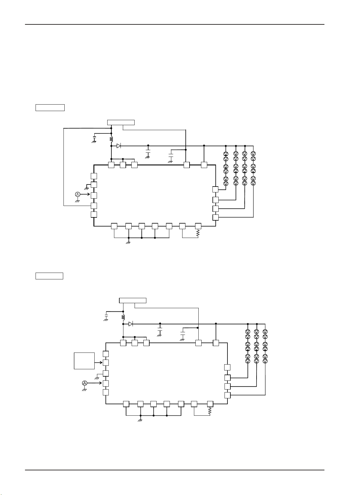
Fig.12 6 series×4 parallel, LED current 20mA setting
Power control PWM application
5inch panel
Battery
2.7V to 5.5V
4.7F
4.7H
Power
ON/OFF
100Hz~10kHz
PWM
SW
TRSW
EN2
EN1
PWM
TESTO
SW
PGND
TEST ISET
Fig.13 6 series×3 parallel, LED current 20mA setting
Current driver PWM application
SW
2.2F
GND
PGND
GND
2.2F
GND
1F
GND
VBAT
GND
1F
VBAT
GND
VDET
LED1
LED2
LED3
LED4
24k
6LED x 4Parallel
Each 20mA
Can be set up to each 10~25mA
6LED x 3Parallel
VDET
LED1
LED2
LED3
LED4
24k
Each 20mA
Can be set up to each 10~25mA
Technical Note
www.rohm.com
© 2011 ROHM Co., Ltd. All rights reserved.
12/19
2011.6 - Rev.C

E
BD6586MUV
●Application example
・LED current setting controlled ISET resistor.
24k : 20mA
30k : 16mA
19.6k : 24.5mA
33k : 14.5mA
・Brightness control
Please input PWM pulse from EN1, EN2 or PWM terminal.
Please refer electrical function p.7.
5 inch panel
Battery
2.7V to 5.5V
4.7F
4.7H
Power
ON/OFF
100Hz~10kHz
PWM
SW
SW
PGND
SW
PGND
TRSW
EN2
EN1
PWM
TESTO
TEST ISET
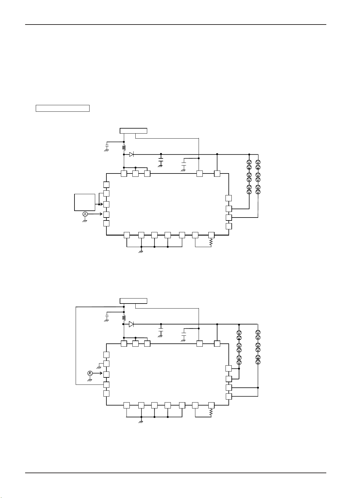
Fig.14 4 series×4 parallel, LED current 20mA setting
Current driver PWM application
Battery
2.7V to 5.5V
Power
ON/O FF
100Hz~ 10kHz
PWM
4.7F
4.7H
SW
SW
SW
TRSW
EN2
EN1
PWM
TESTO
TEST ISET
PGN D
PGND
Fig.15 5 series×3 parallel, LED current 20mA setting
Current driver PWM application
2.2F
GND
2.2F
GND
GND
GND
1F
1F
VBAT
GND
VBAT
GND
VDET
LED1
LED2
LED3
LED4
24k
VDET
LED1
LED2
LED3
LED4
24k
4LED x 4Parallel
Each 20mA
Can be set up to each 10~25mA
5LED x 3Parall el
ach 20mA
Can be set up to each 10~25mA
Technical Note
www.rohm.com
© 2011 ROHM Co., Ltd. All rights reserved.
13/19
2011.6 - Rev.C
BD6586MUV
●Application example
・LED current setting controlled ISET resistor.
24k : 20mA
30k : 16mA
19.6k : 24.5mA
33k : 14.5mA
・Brightness control
Please input PWM pulse from EN1, EN2 or PWM terminal.
Please refer electrical function p.7.
Less than 5 inch panel
Battery
2.7V to 5.5V
4.7F
4.7H
Power
ON/OFF
100Hz~10kHz
PWM
SW
TRSW
EN2
EN1
PWM
TESTO
SW
PGND
TEST ISET
Fig.16 6 series×2 parallel, LED current 20mA setting
Current driver PWM application
Battery
2.7V to 5.5V
4.7F
4.7H
100Hz~1kHz
PWM
SW
TRSW
EN2
EN1
PWM
TESTO
SW
PGND
TEST ISET
Fig.17 6 series×2 parallel, LED current 40mA setting
Power control PWM application
SW
SW
PGND
PGND
2.2F
GND
2.2F
GND
GND
GND
1F
1F
VBAT
GND
VBAT
GND
VDET
LED1
LED2
LED3
LED4
24k
VDET
LED1
LED2
LED3
LED4
24k
6LED x 2Parallel
Each 20mA
Can be set up to each 10~25mA
6LED x 2Parallel
Each 40mA
Can be set up to each 20~50mA
Technical Note
www.rohm.com
© 2011 ROHM Co., Ltd. All rights reserved.
14/19
2011.6 - Rev.C

BD6586MUV
●Application example
・LED current setting controlled ISET resistor.
24k : 20mA
30k : 16mA
19.6k : 24.5mA
33k : 14.5mA
・Brightness control
Please input PWM pulse from EN1, EN2 or PWM terminal.
Please refer electrical function p.7.
Less than 5 inch panel
Battery
2.7V to 5.5V
4.7F
4.7H
Power
ON/OFF
100Hz~10kHz
PWM
SW
SW
PGND
SW
PGND
TRSW
EN2
EN1
PWM
TESTO
TEST ISET
Fig.18 2 series×3 parallel, LED current 20mA setting
Current driver PWM application
Battery
2.7V to 5.5V
4.7F
4.7H
100Hz~1kHz
PWM
TRSW
EN2
EN1
SW
SW
SW
PWM
TESTO
TEST ISET
PGND
PGND
Fig.19 3 series×2 parallel, LED current 40mA setting
Power control PWM application
2.2F
GND
2.2F
GND
GND
GND
1F
1F
VBAT
GND
GND
VBAT
VDET
LED1
LED2
LED3
LED4
24k
VDET
LED1
LED2
LED3
LED4
24k
2LED x 3Parallel
Each 20mA
Can be set up to each 10~25mA
6LED x 2Parallel
Each 40mA
Can be set up to each 20~50mA
Technical Note
www.rohm.com
© 2011 ROHM Co., Ltd. All rights reserved.
15/19
2011.6 - Rev.C

BD6586MUV
●Application example
・LED current setting controlled ISET resistor.
24k : 20mA
30k : 16mA
19.6k : 24.5mA
33k : 14.5mA
・Brightness control
Please input PWM pulse from EN1, EN2 or PWM terminal.
Please refer electrical function p.7.
For big current LED
Battery
2.7V to 5.5V
4.7F
4.7H
Power
ON/OFF
100Hz~10kHz
PWM
SW
SW
PGND
SW
PGND
TRSW
EN2
EN1
PWM
TESTO
TEST ISET
Fig.20 6 series×1 parallel, LED current 60mA setting
Current driver PWM application
Battery
2.7V to 5.5V
4.7F
4.7H
100Hz~1kHz
PWM
SW
SW
PGND
SW
PGND
TRSW
EN2
EN1
PWM
TESTO
TEST ISET
Fig.21 6 series×1 parallel, LED current 80mA setting
Power control PWM application
2.2F
GND
2.2F
GND
GND
GND
1F
GND
1F
VBAT
VBAT
GND
VDET
LED1
LED2
LED3
LED4
24k
VDET
24k
6LED x 1Parallel
Each 60mA
Can be set up to each 30~75mA
6LED x 1Parallel
LED1
LED2
LED3
LED4
Each 80mA
Can be set up to each 40~100mA
Technical Note
www.rohm.com
© 2011 ROHM Co., Ltd. All rights reserved.
16/19
2011.6 - Rev.C

E
A
BD6586MUV
●Application example
・LED current setting controlled ISET resistor.
24k : 20mA
30k : 16mA
19.6k : 24.5mA
33k : 14.5mA
・Brightness control
Please input PWM pulse from EN1, EN2 or PWM terminal.
Please refer electrical function p.7.
For the application of 7V and more
Other Power Supply
6.0Vto25V
4.7F
Power
ON/OFF
4.7H
2.2F
SW
SW
TRSW
EN2
EN1
PWM
TESTO
TEST ISET
PGND
SW
PGND
GND
GND
Fig.22 6 series×4 parallel, LED current 20mA setting
Power control PWM application
●Analog style optical application
Control LED current to charged D/A voltage.
Show application example and typ control.
Please decide final value after you evaluated application, characteristic.
Power
ON/O FF
Battery
2.7V to 5.5V
4.7F
4.7H
2.2F
SW
SW
SW
TRSW
EN2
EN1
PWM
TESTO
PGND
GND
PGND
TEST ISET
GND
1F
VBAT
GND
6LED x 4Parallel
VDET
LED1
LED2
LED3
LED4
ach 20mA
Can be set up to each 10~25mA
470
24k
D/A
Fig.23 Analog style optical application
Battery
2.7V to 5.5V
1F
VDET
VBAT
LED1
LED2
LED3
GND
LED4
24k
D/A LED current
0.05V 19.4mA
0.2V 14.4mA
0.4V 7.7mA
0.5V 4.4mA
0.6V 1.0mA
0.7V 0mA
LED current =
typ LED current =
6LED x 4Parallel
Each 20mA
Can be set up to each 20~50mA
ISET voltage
470k
0.6V
470k
ISET voltage -D/
+
0.6V-D/A
+
Technical Note
24k
24k
×800
×800
www.rohm.com
© 2011 ROHM Co., Ltd. All rights reserved.
17/19
2011.6 - Rev.C

BD6586MUV
●Notes for use
(1) Absolute Maximum Ratings
An excess in the absolute maximum ratings, such as supply voltage, temperature range of operating conditions, etc., can
break down devices, thus making impossible to identify breaking mode such as a short circuit or an open circuit. If any
special mode exceeding the absolute maximum ratings is assumed, consideration should be given to take physical safety
measures including the use of fuses, etc.
(2) Operating conditions
These conditions represent a range within which characteristics can be provided approximately as expected. The
electrical characteristics are guaranteed under the conditions of each parameter.
(3) Reverse connection of power supply connector
The reverse connection of power supply connector can break down ICs. Take protective measures against the breakdown
due to the reverse connection, such as mounting an external diode between the power supply and the IC’s power supply
terminal.
(4) Power supply line
Design PCB pattern to provide low impedance for the wiring between the power supply and the GND lines. In this regard,
for the digital block power supply and the analog block power supply, even though these power supplies has the same
level of potential, separate the power supply pattern for the digital block from that for the analog block, thus suppressing
the diffraction of digital noises to the analog block power supply resulting from impedance common to the wiring patterns.
For the GND line, give consideration to design the patterns in a similar manner.
Furthermore, for all power supply terminals to ICs, mount a capacitor between the power supply and the GND terminal. At
the same time, in order to use an electrolytic capacitor, thoroughly check to be sure the characteristics of the capacitor to
be used present no problem including the occurrence of capacity dropout at a low temperature, thus determining the
constant.
(5) GND voltage
Make setting of the potential of the GND terminal so that it will be maintained at the minimum in any operating state.
Furthermore, check to be sure no terminals are at a potential lower than the GND voltage including an actual electric transient.
(6) Short circuit between terminals and erroneous mounting
In order to mount ICs on a set PCB, pay thorough attention to the direction and offset of the ICs. Erroneous mounting can
break down the ICs. Furthermore, if a short circuit occurs due to foreign matters entering between terminals or between
the terminal and the power supply or the GND terminal, the ICs can break down.
(7) Operation in strong electromagnetic field
Be noted that using ICs in the strong electromagnetic field can malfunction them.
(8) Inspection with set PCB
On the inspection with the set PCB, if a capacitor is connected to a low-impedance IC terminal, the IC can suffer stress.
Therefore, be sure to discharge from the set PCB by each process. Furthermore, in order to mount or dismount the set
PCB to/from the jig for the inspection process, be sure to turn OFF the power supply and then mount the set PCB to the jig.
After the completion of the inspection, be sure to turn OFF the power supply and then dismount it from the jig. In addition,
for protection against static electricity, establish a ground for the assembly process and pay thorough attention to the
transportation and the storage of the set PCB.
(9) Input terminals
In terms of the construction of IC, parasitic elements are inevitably formed in relation to potential. The operation of the
parasitic element can cause interference with circuit operation, thus resulting in a malfunction and then breakdown of the
input terminal. Therefore, pay thorough attention not to handle the input terminals, such as to apply to the input terminals a
voltage lower than the GND respectively, so that any parasitic element will operate. Furthermore, do not apply a voltage to
the input terminals when no power supply voltage is applied to the IC. In addition, even if the power supply voltage is
applied, apply to the input terminals a voltage lower than the power supply voltage or within the guaranteed value of
electrical characteristics.
(10) Ground wiring pattern
If small-signal GND and large-current GND are provided, It will be recommended to separate the large-current GND
pattern from the small-signal GND pattern and establish a single ground at the reference point of the set PCB so that
resistance to the wiring pattern and voltage fluctuations due to a large current will cause no fluctuations in voltages of the
small-signal GND. Pay attention not to cause fluctuations in the GND wiring pattern of external parts as well.
(11) External capacitor
In order to use a ceramic capacitor as the external capacitor, determine the constant with consideration given to a
degradation in the nominal capacitance due to DC bias and changes in the capacitance due to temperature, etc.
(12) Thermal shutdown circuit (TSD)
When junction temperatures become 175°C (typ) or higher, the thermal shutdown circuit operates and turns a switch OFF.
The thermal shutdown circuit, which is aimed at isolating the LSI from thermal runaway as much as possible, is not aimed
at the protection or guarantee of the LSI. Therefore, do not continuously use the LSI with this circuit operating or use the
LSI assuming its operation.
(13) Thermal design
Perform thermal design in which there are adequate margins by taking into account the permissible dissipation (Pd) in
actual states of use.
(14) Selection of coil
Select the low DCR inductors to decrease power loss for DC/DC converter.
Technical Note
www.rohm.com
© 2011 ROHM Co., Ltd. All rights reserved.
18/19
2011.6 - Rev.C

BD6586MUV
●Ordering part number
Technical Note
B D
Part No. Part No.
VQFN024V4040
4.0±0.1
1.0MAX
0.08 S
C0.2
24
19
0.4±0.1
0.75
6 5 8 6
6586
4.0±0.1
1PIN MARK
2.4±0.1
16
0.5
S
0.02
-
+0.03
(0.22)
0.02
7
2.4±0.1
12
1318
+0.05
0.25
-
0.04
(Unit : mm)
MU V
Package
MUV: VQFN024V4040
<Tape and Reel information>
Embossed carrier tapeTape
Quantity
Direction
of feed
2500pcs
E2
The direction is the 1pin of product is at the upper left when you hold
()
reel on the left hand and you pull out the tape on the right hand
Reel
-
E 2
Packaging and forming specification
E2: Embossed tape and reel
1pin
Order quantity needs to be multiple of the minimum quantity.
∗
Direction of feed
www.rohm.com
© 2011 ROHM Co., Ltd. All rights reserved.
19/19
2011.6 - Rev.C

Notes
No copying or reproduction of this document, in par t or in whole, is permitted without the
consent of ROHM Co.,Ltd.
The content specied herein is subject to change for improvement without notice.
The content specied herein is for the purpose of introducing ROHM's products (hereinafter
"Products"). If you wish to use any such Product, please be sure to refer to the specications,
which can be obtained from ROHM upon request.
Examples of application circuits, circuit constants and any other information contained herein
illustrate the standard usage and operations of the Products. The peripheral conditions must
be taken into account when designing circuits for mass production.
Great care was taken in ensuring the accuracy of the information specied in this document.
However, should you incur any damage arising from any inaccuracy or misprint of such
information, ROHM shall bear no responsibility for such damage.
The technical information specied herein is intended only to show the typical functions of and
examples of application circuits for the Products. ROHM does not grant you, explicitly or
implicitly, any license to use or exercise intellectual property or other rights held by ROHM and
other parties. ROHM shall bear no responsibility whatsoever for any dispute arising from the
use of such technical information.
The Products specied in this document are intended to be used with general-use electronic
equipment or devices (such as audio visual equipment, ofce-automation equipment, communication devices, electronic appliances and amusement devices).
The Products specied in this document are not designed to be radiation tolerant.
While ROHM always makes effor ts to enhance the quality and reliability of its Products, a
Product may fail or malfunction for a variety of reasons.
Please be sure to implement in your equipment using the Products safety measures to guard
against the possibility of physical injury, re or any other damage caused in the event of the
failure of any Product, such as derating, redundancy, re control and fail-safe designs. ROHM
shall bear no responsibility whatsoever for your use of any Product outside of the prescribed
scope or not in accordance with the instruction manual.
The Products are not designed or manufactured to be used with any equipment, device or
system which requires an extremely high level of reliability the failure or malfunction of which
may result in a direct threat to human life or create a risk of human injury (such as a medical
instrument, transportation equipment, aerospace machinery, nuclear-reactor controller, fuelcontroller or other safety device). ROHM shall bear no responsibility in any way for use of any
of the Products for the above special purposes. If a Product is intended to be used for any
such special purpose, please contact a ROHM sales representative before purchasing.
If you intend to export or ship overseas any Product or technology specied herein that may
be controlled under the Foreign Exchange and the Foreign Trade Law, you will be required to
obtain a license or permit under the Law.
Notice
www.rohm.com
© 2011 ROHM Co., Ltd. All rights reserved.
Thank you for your accessing to ROHM product informations.
More detail product informations and catalogs are available, please contact us.
ROHM Customer Support System
http://www.rohm.com/contact/
R1120
A
 Loading...