

Page 1

Power Management Switch ICs for PCs and Digital Consumer Products
Load Switch ICs
for Portable Equipment
BD6528HFV,BD6529GUL
●Description
Power switch for memory card Slot (BD6528HFV, BD6529GUL) is a high side switch IC having one circuit of N-channel
Power MOSFET. This switch IC achieves ON resistance of 100mΩ with BD6529GUL; and 110mΩ with BD6528HFV.
Operations from low input voltage (VIN≦2.7V) is possible; made for use of various switch applications. BD6524HFV is
available in a space-saving HVSOF6 package. BD6529GUL is available in a space-saving VCSP-6 package.
●Features
1) Single channel of Low On-Resistance (Typ. = 100mΩ) N-channel MOSFET built in
2) 500mA output current
3) Low voltage switch capability
4) Soft-start function
5) Output discharge circuit
6) Reverse current flow blocking at switch off
7) HVSOF6 package for BD6528HFV
VCSP50L1 package for BD6529GUL
●Applications
Memory card slots of Mobile phone, Digital still camera, PDA, MP3 player, PC, etc.
●Line up matrix
Part Number ON resistance Output current Discharge circuit Logic Control Input Package
BD6528HFV 110mΩ 500mA ○ High
BD6529GUL 100mΩ 500mA ○ High
●Absolute maximum ratings
No.11029ECT19
HVSOF6
1.6 x 3.0 mm
VCSP50L1
1.5 x 1.0 mm
Parameter Symbol Ratings Unit
Supply voltage VDD -0.3 ~ 6.0 V
VIN voltage VIN -0.3 ~ 6.0 V
EN voltage VEN -0.3 ~ VDD + 0.3 V
VOUT voltage VOUT -0.3 ~ 6.0 V
Storage temperature TSTG -55 ~ 150 ℃
Power dissipation Pd
*1 Mounted on 70mm * 70mm * 1.6mm Glass-epoxy PCB. Derating: 6.8mW /℃ at Ta > 25℃
*2 Mounted on 50mm * 58mm * 1.75mm Glass-epoxy PCB. Derating: 4.6mW / ℃ at Ta > 25℃
* This product is not designed for protection against radioactive rays.
* Operation is not guaranteed.
●Operating conditions
Parameter Symbol
Operating voltage VDD 2.7 3.3 4.5 V
Switch input voltage VIN 0 1.2 2.7 V
Operation temperature TOPR -25 25 85 ℃
Output current ILO 0 - 500 mA
849 *1 (BD6528HFV)
575 *2 (BD6529GUL)
Ratings
Min. Typ. Max.
mW
Unit
www.rohm.com
© 2011 ROHM Co., Ltd. All rights reserved.
1/11
2011.05 - Rev.C
Page 2
BD6528HFV,BD6529GUL
●Electrical characteristics
○BD6528HFV(unless otherwise specified, VDD =3.3V, VIN = 1.2V, Ta = 25℃)
Parameter Symbol
[Current consumption]
Operating current IDD - 20 30 µA VEN = 1.2V
Standby current ISTB - 0.01 1 µA VEN = 0V
[I/O]
EN input voltage
EN input current IEN -1 - 1 µA VEN = 0V or VEN = 1.2V
[Power switch]
On-resistance RON - 110 - mΩ IOUT = 500mA
Switch leakage current ILEAK - 0.01 10 µA VEN = 0V, VOUT = 0V
Output rise time TON1 - 0.5 1 ms RL = 10Ω, VOUT 10% → 90%
Output turn-on time TON2 - 0.6 2 ms RL = 10Ω, VEN High →VOUT 90%
Output fall time TOFF1 - 1 20 µs RL = 10Ω, VOUT 90% → 10%
Output turn-off time TOFF2 - 15 100 µs RL = 10Ω, VEN Low →VOUT 10%
[Discharge circuit]
Discharge on-resistance RDISC - 70 110 Ω IOUT = -1mA, VEN = 0V
Parameter IDISC - 15 20 mA VOUT = 3.3V, VEN = 0V
○BD6529GUL(unless otherwise specified, V
Parameter Symbol
[Current consumption]
Operating current IDD - 20 30 µA VEN = 1.2V
Standby current ISTB - 0.01 1 µA VEN = 0V
[I/O]
EN input voltage
EN input current IEN -1 - 1 µA VEN = 0V or VEN = 1.2V
[Power switch]
On Resistance RON - 100 - mΩ IOUT = 500mA
Switch leakage current ILEAK - 0.01 10 µA VEN = 0V, VOUT = 0V
Output turn on rise time TON1 - 0.5 1 ms RL = 10Ω, VOUT 10% → 90%
Output turn on time TON2 - 0.6 2 ms RL = 10Ω, VEN High →VOUT 90%
Output turn off fall time TOFF1 - 0.1 4 µs RL = 10Ω, VOUT 90% → 10%
Output turn off time TOFF2 - 1 6 µs RL = 10Ω, VEN Low →VOUT 10%
[Discharge circuit]
Discharge on-resistance RDISC - 70 110 Ω IOUT = -1mA, VEN = 0V
Discharge current IDISC - 15 20 mA VOUT = 3.3V, VEN = 0V
VENH 1.2 - - V High level input
VENL - - 0.4 V Low level input
VENH 1.2 - - V High level input
VENL - - 0.4 V Low level input
Min. Typ. Max.
DD =3.3V, VIN = 1.2V, Ta = 25℃)
Min. Typ. Max.
Limits
Limits
Unit Condition
Unit Condition
Technical Note
www.rohm.com
© 2011 ROHM Co., Ltd. All rights reserved.
2/11
2011.05 - Rev.C
Page 3
BD6528HFV,BD6529GUL
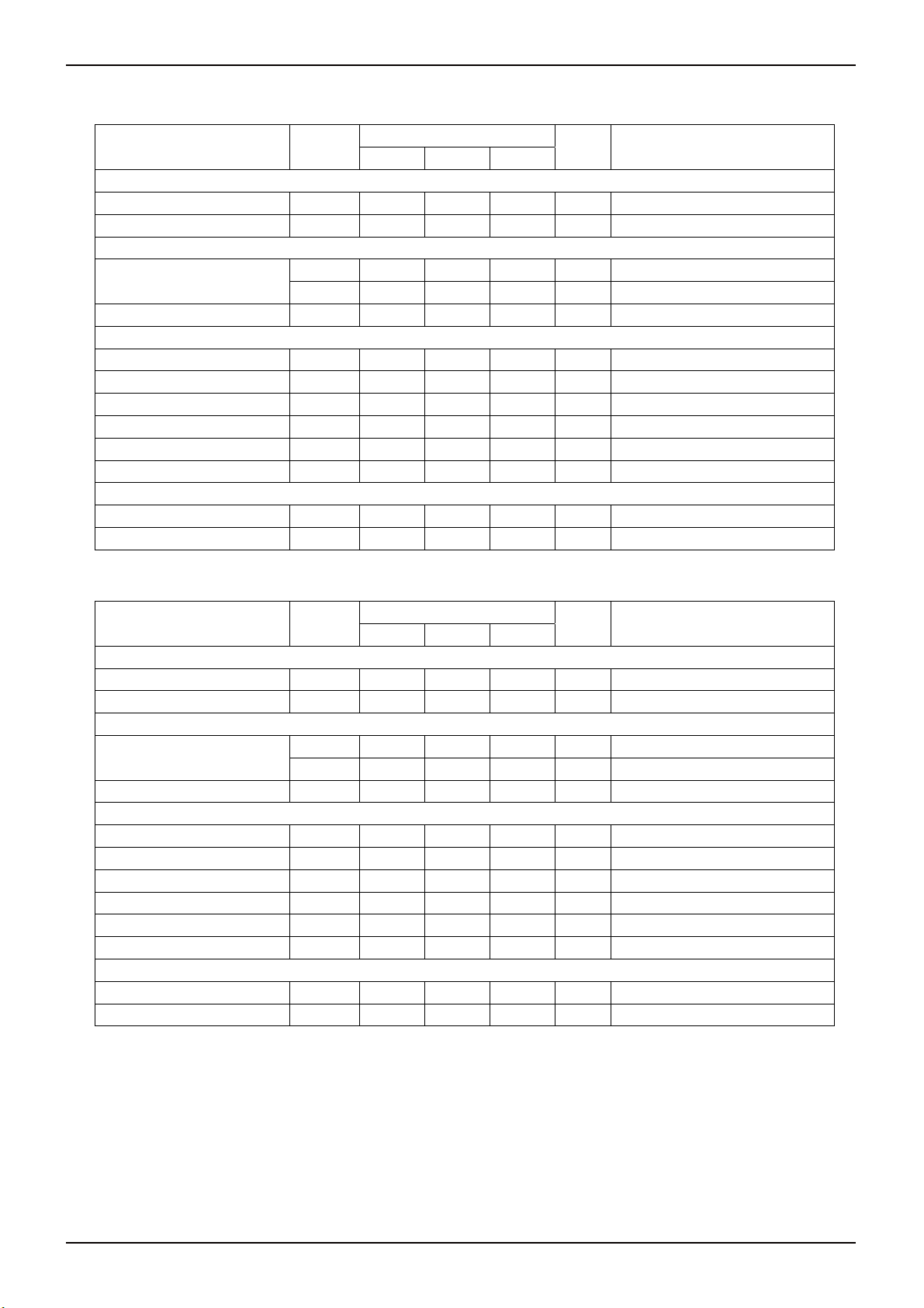
●Test circuit
●Switch output turn ON/OFF timing
VINVDDV
V
EN
V
OUT
EN
VIN
VDD
EN
VOUT
VOUT
GND
Fig.1 Measurement circuit
50% 50%
T
ON2
90%
10%
T
ON1
Fig.2 Timing diagrams
90%
T
RL
OFF2
10%
T
Technical Note
CL
OFF1
www.rohm.com
© 2011 ROHM Co., Ltd. All rights reserved.
3/11
2011.05 - Rev.C
Page 4

BD6528HFV,BD6529GUL
●Reference data
30
OPERATING CURRENT :
Ta= 2 5º C
25
20
[µA]
15
DD
I
10
5
0
23 45
SUPPLY VOLT AGE : V
[V]
DD
Fig.3 Operating current
EN enable
1.0
VDD=3.3V
0.8
0.6
[uA]
STB
I
0.4
STANDBY CURRENT :
0.2
0.0
-50 0 50 100
AMBIEN T T EMPER ATU RE : T a [°C]
Fig.6 Standby current
EN disable
200
ON RESISTANCE :
Ta= 2 5º C
V
=1.2V
IN
150
I
=100mA
OUT
]
Ω
[m
100
ON
R
50
0
23 45
SUPPLY VOLT AGE : V
[V]
DD
Fig.9 On-resistance vs. VDD
(BD6528HFV)
200.0
150.0
100.0
50.0
VDD=3.3V
V
=1.2V
IN
Ta= 8 5º C
Ta= 2 5º C
Ta= - 25 ºC
]
Ω
[m
ON
R
ON RESISTANCE :
0.0
0 200 400 600
OUTPUT CURRENT : I
OUT
[mA]
Fig.12 On-resistance vs. IOUT
(BD6528HFV)
30
VDD=3.3V
25
20
[μA]
15
DD
I
10
OPERATING CURRENT :
5
0
-50 0 50 100
AMBIENT TEMPER ATUR E : Ta [°C]
ON RESISTANCE :
Fig.4 Operating current
EN enable
2.0
Ta= 2 5º C
1.5
1.0
VEN [V]
0.5
ENABLE IN PUT VOLT AGE:
0.0
23 45
SUPPLY VOLT AGE : V
[V]
DD
Fig.7 EN input voltage
200
VDD=3.3V
V
=1.2V
IN
150
I
=100mA
OUT
]
Ω
[m
100
ON
R
50
0
-50 0 50 100
AMBIEN T T EMPER ATU RE : T a [°C]
Fig.10 On-resistance vs. temperature
(BD6528HFV)
200
Ta= 2 5º C
V
=1.2V
IN
150
I
=100mA
OUT
]
Ω
[m
100
ON
R
ON RESISTANCE :
50
0
2345
SUPPLY VOLT AGE : V
[V]
DD
Fig.13 On-resistance vs. V
(BD6529GUL)
DD
Technical Note
1.0
Ta= 2 5º C
0.8
0.6
[uA]
STB
I
0.4
STANDBY CURRENT :
0.2
0.0
2345
SUPPLY VOLT AGE : V
Fig.5 Standby current
EN disable
2.0
VDD=3.3V
1.5
[V]
1.0
EN
V
0.5
ENABLE INPU T VOLTAGE :
0.0
-50 0 50 100
AMBIENT TEM PERATU RE : Ta [°C ]
Fig.8 EN input voltage
200
VDD=3.3V
I
=100mA
OUT
150
Ta= 8 5º C
]
Ω
[m
100
Ta= 2 5º C
ON
R
ON R ESISTANC E :
Ta= - 25 ºC
50
0
0123
INPU T VOLTAGE : V
Fig.11 On-resistance vs. VIN
(BD6528HFV)
200
VDD=3.3V
V
=1.2V
IN
150
I
=100mA
OUT
]
Ω
[m
100
ON
R
ON RESISTANCE :
50
0
-50 0 50 100
AMBIENT TEM PERATUR E : Ta [°C]
Fig.14 On-resistance vs. temperature
(BD6529GUL)
[V]
DD
[V]
IN
www.rohm.com
© 2011 ROHM Co., Ltd. All rights reserved.
4/11
2011.05 - Rev.C
Page 5

BD6528HFV,BD6529GUL
200
ON RESISTANCE :
VDD=3.3V
I
=100mA
OUT
150
]
Ta= 8 5º C
Ω
100
[m
ON
Ta= 2 5º C
R
Ta= - 25 ºC
50
0
0123
INPUT VOLTAGE : V
Fig.15 On-resistance vs. VIN
(BD6529GUL)
[V]
IN
1
0.8
VDD=3.3V
RL=10
Ω
0.6
[ms]
ON1
T
0.4
RISE TIME :
0.2
0
-50 0 50 100
AMBIEN T T EMPER ATU RE : T a [°C]
Fig.18 Output rise time
1.0
0.8
Ta= 2 5º C
RL=10
Ω
0.6
[us]
OFF1
T
0.4
FALL TIME :
0.2
0.0
2345
SUPPLY VOLTAGE : V
[V]
DD
Fig.21 Output fall time
50
VDD=3.3V
Ω
RL=10
40
30
[us]
OFF2
T
20
TURN OFF TIME :
10
BD6529GUL
0
-50 0 50 100
AMBIENT TEMPERATURE : Ta [°C]
Fig.24 Output turn-off time
BD6528HFV
200
VDD=3.3V
V
=1.2V
IN
150
]
Ω
[m
100
ON
R
ON RESISTANCE :
50
0
0 200 400 600
OUTPUT CURRENT : I
Fig.16 On-resistance vs. IOUT
(BD6529GUL)
2.0
Ta= 2 5º C
RL=10
1.6
1.2
[ms]
ON2
T
0.8
TURN ON TIME :
0.4
0.0
2345
Ω
SUPPLY VOLT AGE : V
Fig.19 Output turn-on time
1.0
VDD=3.3V
Ω
RL=10
0.8
0.6
[us]
OFF1
T
0.4
FALL TIME :
0.2
0.0
-50 0 50 100
AMBIEN T T EMPER ATU RE : T a [°C]
Fig.22 Output fall time
200
VDD=3.3V
150
[Ω]
100
DISC
R
50
DISCHARSE ON RESISTANCE :
0
2345
SUPPLY VOLTAGE : V
Fig.25 Discharge on-resistance
OUT
Technical Note
1.0
Ta= 2 5º C
RL=10
0.8
Ta= 8 5º C
Ta= 2 5º C
Ta= - 25 ºC
[mA]
[V]
DD
[V]
DD
0.6
[ms]
ON1
T
0.4
RISE TIME :
0.2
0.0
2.0
1.6
1.2
[ms]
ON2
T
0.8
TURN ON TIME :
0.4
0.0
50
40
30
[us]
OFF2
T
20
TURN OFF TIME :
10
0
200
150
[O]
100
DISC
R
50
DISCHARSE ON RESISTANCE :
0
Fig.26 Discharge on-resistance
Ω
23 45
SUPPLY VOLTAGE : V
[V]
DD
Fig.17 Output rise time
VDD=3.3V
RL=10
Ω
-50 0 50 100
AMBIENT TEM PERATU RE : Ta [°C ]
Fig.20 Output turn-on time
Ta= 2 5º C
Ω
RL=10
BD6528HFV
BD6529GUL
23 45
SUPPLY VOLT AGE : V
[V]
DD
Fig.23 Output turn-off time
Ta= 2 5º C
-50 0 50 100
AMBIENT TEM PERATU RE : Ta [°C ]
www.rohm.com
© 2011 ROHM Co., Ltd. All rights reserved.
5/11
2011.05 - Rev.C
Page 6

BD6528HFV,BD6529GUL
●Waveform data
VEN
(0.5V/div.)
V
OUT
(0.2V/div.)
OUT
I
(10mA/div.)
Fig.27 Output turn-on response
TIME (0.2ms/div.)
BD6528HFV
V
DD
V
IN=1.2V
=500Ω
R
L
C
=4.7uF
L
=3.3V
VEN
(0.5V/div.)
V
OUT
(0.2V/div.)
V
DD
V
IN=1.2V
=10Ω
R
L
C
=4.7uF
L
=3.3V
OUT
I
(50mA/div.)
Fig.29 Output turn-on response
TIME (0.2ms/div.)
BD6528HFV
V
EN
(0.5V/div.)
V
OUT
(0.2V/div.)
OUT
I
(10mA/div.)
VDD=3.3V
V
IN=1.2V
=500Ω
R
L
=4.7µF
C
L
Fig.31 Output turn-on response
TIME (0.2ms/div.)
BD6529GUL
V
EN
(0.5V/div.)
V
OUT
(0.2V/div.)
V
DD
V
IN=1.2V
=10Ω
R
L
C
=4.7µF
L
=3.3V
OUT
I
(50mA/div.)
Fig.33 Output turn-on response
TIME (0.2ms/div.)
BD6529GUL
V
EN
(0.5V/div.)
V
OUT
(0.2V/div.)
OUT
I
(10mA/div.)
TIME (0.2ms/div.)
Fig.28 Output turn-off response
BD6528HFV
EN
V
(0.5V/div.)
V
OUT
(0.2V/div.)
OUT
I
(50mA/div.)
TIME (0.2ms/div.)
Fig.30 Output turn-off response
BD6528HFV
EN
V
(0.5V/div.)
V
OUT
(0.2V/div.)
OUT
I
(10mA/div.)
TIME (0.2ms/div.)
Fig.32 Output turn-off response
BD6529GUL
V
EN
(0.5V/div.)
V
OUT
(0.2V/div.)
OUT
I
(50mA/div.)
TIME (0.2ms/div.)
Fig.34 Output turn-off response
BD6529GUL
VDD=3.3V
V
IN=1.2V
=500Ω
R
L
C
=4.7uF
L
=3.3V
V
DD
V
IN=1.2V
=10Ω
R
L
C
=4.7uF
L
V
=3.3V
DD
V
IN=1.2V
=500Ω
R
L
=4.7µF
C
L
V
=3.3V
DD
V
IN=1.2V
=10Ω
R
L
C
=4.7µF
L
EN
V
(2V/div.)
V
OUT
(1V/div.)
OUT
I
(20mA/div.)
Technical Note
IN=1.2V
V
DD=3.3V
V
L=22µF
C
CL=10uF
L=4.7uF
C
Fig.35 Rush current response
TIME (0.2ms/div.)
www.rohm.com
© 2011 ROHM Co., Ltd. All rights reserved.
6/11
2011.05 - Rev.C
Page 7

BD6528HFV,BD6529GUL
●Block diagram
VIN
VDD
EN
Fig.36 Block diagram Fig.37 Pin configuration
●Pin description
charge
pump
VOUT
GND
B VIN VOUT VOUT
A VDD EN GND
1 2 3
BD6529GUL (Bottom view)
BD6528HFV (Top view)
Technical Note
Pin number Pin name Pin function
1
(A3)
2, 3
(B2, B3)
4
(B1)
5
(A1)
6
(A2)
●I/O equivalent circuit
Pin name Pin number Equivalent circuit
EN
GND Ground
VOUT
VIN Switch input
VDD
EN
6
(A2)
Switch output
(connect each pin externally)
Power supply
(for switch control and drive circuit)
Enable input
(Active-High Switch on input)
VDD
EN
VIN
VOUT
www.rohm.com
© 2011 ROHM Co., Ltd. All rights reserved.
4
(B1)
2, 3
(B2, B3)
VIN
7/11
VOUT
2011.05 - Rev.C
Page 8
BD6528HFV,BD6529GUL
●Operation description
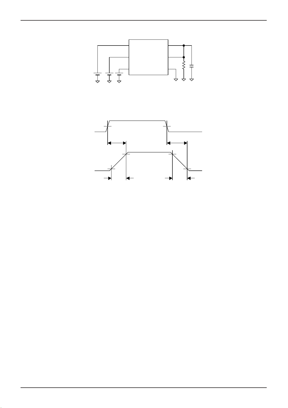
1. Switch operation
Each VIN and VOUT pins are connected to MOSFET’s drain and source. By setting EN input to High level, the internal
charge pump operates and turns on MOSFET.
When MOSFET is turned on, the switch becomes bidirectional characteristics. Consequently, in case of VIN < VOUT, the
current is flowing from VOUT to VIN.
Since there is no parasitic diode between switch’s drain and source, it prevents the reverse current flow from VOUT to
VIN during switch off stage.
2. Output discharge circuit
Discharge circuit operates when switch is off. When discharge circuit operates, 70Ω (Typ.) resistor is connected between
VOUT pin and GND pin. This discharges the electrical charge quickly.
●Application circuit example
* This application circuit does not guarantee its operation.
When the external circuit constant, etc. is changed, be sure to consider adequate margins; by taking into account
external parts and/or IC’s dispersion including not only static characteristics, but also transient characteristics.
Discharge circuit
VINV
DD
VDD
VIN
EN
VOUT
ON ONOFF OFF
Fig.38 Operation timing
VIN
VDD
ON / OFF
Fig.39 Application circuit example
EN
ON
LOAD
VOUT
VOUT
GND
Technical Note
www.rohm.com
© 2011 ROHM Co., Ltd. All rights reserved.
8/11
2011.05 - Rev.C
Page 9

BD6528HFV,BD6529GUL
●Power dissipation characteristics
900
800
700
600
500
400
300
POWER DISSIPATION : Pd [mW]
200
100
0
0 25 50 75 100 125 150
700
600
500
400
300
200
POWER DISSIPATION : Pd [mW]
100
0
0 25 50 75 100 125 150
Technical Note
AMBIENT TEMPERATURE : Ta [℃]
Fig.40 Power dissipation curve (Pd-Ta Curve)
(HVSOF6 package)
AMBIENT TEMPERATURE : Ta [℃]
Fig.41 Power dissipation curve (Pd-Ta Curve)
(VCSP50L1 package)
www.rohm.com
© 2011 ROHM Co., Ltd. All rights reserved.
9/11
2011.05 - Rev.C
Page 10

BD6528HFV,BD6529GUL
●Notes foe use
Technical Note
(1) Absolute Maximum Ratings
An excess in the absolute maximum ratings, such as supply voltage, temperature range of operating conditions, etc., can
break down devices, thus making impossible to identify breaking mode such as a short circuit or an open circuit. If any
special mode exceeding the absolute maximum ratings is assumed, consideration should be given to take physical safety
measures including the use of fuses, etc.
(2) Power supply and GND line
Design PCB pattern to provide low impedance for the wiring between the power supply and the GND lines. Pay attention
to the interference by common impedance of layout pattern when there are plural power supplies and GND lines.
Especially, when there are GND pattern for small signal and GND pattern for large current included the external circuits,
separate each GND pattern. Furthermore, for all power supply terminals to ICs, mount a capacitor between the power
supply and the GND terminal. At the same time, in order to use a capacitor, thoroughly check to be sure the
characteristics of the capacitor to be used present no problem including the occurrence of capacity dropout at a low
temperature, thus determining the constant.
(3) GND voltage
Make setting of the potential of the GND terminal so that it will be maintained at the minimum in any operating state.
Furthermore, check to be sure no terminals are at a potential lower than the GND voltage including an actual electric
transient.
(4) Short circuit between terminals and erroneous mounting
In order to mount ICs on a set PCB, pay thorough attention to the direction and offset of the ICs. Erroneous mounting can
break down the ICs. Furthermore, if a short circuit occurs due to foreign matters entering between terminals or between
the terminal and the power supply or the GND terminal, the ICs can break down.
(5) Operation in strong electromagnetic field
Be noted that using ICs in the strong electromagnetic field can malfunction them.
(6) Input terminals
In terms of the construction of IC, parasitic elements are inevitably formed in relation to potential. The operation of the
parasitic element can cause interference with circuit operation, thus resulting in a malfunction and then breakdown of the
input terminal. Therefore, pay thorough attention not to handle the input terminals, such as to apply to the input terminals
a voltage lower than the GND respectively, so that any parasitic element will operate. Furthermore, do not apply a voltage
to the input terminals when no power supply voltage is applied to the IC. In addition, even if the power supply voltage is
applied, apply to the input terminals a voltage lower than the power supply voltage or within the guaranteed value of
electrical characteristics.
(7) External capacitor
In order to use a ceramic capacitor as the external capacitor, determine the constant with consideration given to a
degradation in the nominal capacitance due to DC bias and changes in the capacitance due to temperature, etc.
(8) Thermal design
Perform thermal design in which there are adequate margins by taking into account the power dissipation (PD) in actual
states of use.
www.rohm.com
© 2011 ROHM Co., Ltd. All rights reserved.
10/11
2011.05 - Rev.C
Page 11
BD6528HFV,BD6529GUL
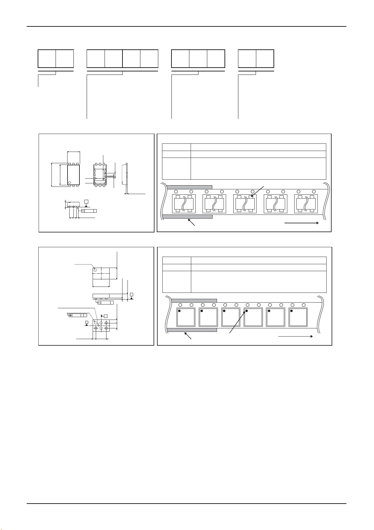
●Ordering part number
B D 6 5 2 8 H F V - T R
Part No. Part No.
HVSOF6
1.6±0.1
(MAX 1.8 include BURR)
3.0±0.1
456
0.1
2.6±
321
(MAX 2.8 include BURR)
0.75Max.
0.5
VCSP50L1
(BD6529GUL)
1PIN MARK
(φ0.15)INDEX POST
6-φ0.25±0.05
0.05
0.25±0.05
(1.2)
(1.4)
S
0.1 S
0.22±0.05
BA
B
B
A
6528
6529
1.50±0.05
1
P=0.5×2
(1.5)
0.08 S
2
(0.45)
(0.15)
0.145±0.05
(Unit : mm)
1.00±0.05
0.10±0.05
0.55MAX
S
A
0.25±0.05
0.5
3
(Unit : mm)
Package
HFV: HVSOF6
GUL: VCSP50L1
<Tape and Reel information>
Embossed carrier tapeTape
Quantity
Direction
of feed
<Tape and Reel information>
Quantity
Direction
of feed
3000pcs
TR
The direction is the 1pin of product is at the upper right when you hold
()
reel on the left hand and you pull out the tape on the right hand
Reel
Embossed carrier tape(heat sealing method)Tape
3000pcs
E2
The direction is the 1pin of product is at the upper left when you hold
()
reel on the left hand and you pull out the tape on the right hand
Reel
Packaging and forming specification
TR: Embossed tape and reel
(HVSOF6)
E2: Embossed tape and reel
(VCSP50L1)
Order quantity needs to be multiple of the minimum quantity.
∗
1pin
Order quantity needs to be multiple of the minimum quantity.
∗
Technical Note
1pin
Direction of feed
Direction of feed
www.rohm.com
© 2011 ROHM Co., Ltd. All rights reserved.
11/11
2011.05 - Rev.C
Page 12

Notes
No copying or reproduction of this document, in par t or in whole, is permitted without the
consent of ROHM Co.,Ltd.
The content specied herein is subject to change for improvement without notice.
The content specied herein is for the purpose of introducing ROHM's products (hereinafter
"Products"). If you wish to use any such Product, please be sure to refer to the specications,
which can be obtained from ROHM upon request.
Examples of application circuits, circuit constants and any other information contained herein
illustrate the standard usage and operations of the Products. The peripheral conditions must
be taken into account when designing circuits for mass production.
Great care was taken in ensuring the accuracy of the information specied in this document.
However, should you incur any damage arising from any inaccuracy or misprint of such
information, ROHM shall bear no responsibility for such damage.
The technical information specied herein is intended only to show the typical functions of and
examples of application circuits for the Products. ROHM does not grant you, explicitly or
implicitly, any license to use or exercise intellectual property or other rights held by ROHM and
other parties. ROHM shall bear no responsibility whatsoever for any dispute arising from the
use of such technical information.
The Products specied in this document are intended to be used with general-use electronic
equipment or devices (such as audio visual equipment, ofce-automation equipment, communication devices, electronic appliances and amusement devices).
The Products specied in this document are not designed to be radiation tolerant.
While ROHM always makes effor ts to enhance the quality and reliability of its Products, a
Product may fail or malfunction for a variety of reasons.
Please be sure to implement in your equipment using the Products safety measures to guard
against the possibility of physical injury, re or any other damage caused in the event of the
failure of any Product, such as derating, redundancy, re control and fail-safe designs. ROHM
shall bear no responsibility whatsoever for your use of any Product outside of the prescribed
scope or not in accordance with the instruction manual.
The Products are not designed or manufactured to be used with any equipment, device or
system which requires an extremely high level of reliability the failure or malfunction of which
may result in a direct threat to human life or create a risk of human injury (such as a medical
instrument, transportation equipment, aerospace machiner y, nuclear-reactor controller, fuelcontroller or other safety device). ROHM shall bear no responsibility in any way for use of any
of the Products for the above special purposes. If a Product is intended to be used for any
such special purpose, please contact a ROHM sales representative before purchasing.
If you intend to export or ship overseas any Product or technology specied herein that may
be controlled under the Foreign Exchange and the Foreign Trade Law, you will be required to
obtain a license or permit under the Law.
Notice
www.rohm.com
© 2011 ROHM Co., Ltd. All rights reserved.
Thank you for your accessing to ROHM product informations.
More detail product informations and catalogs are available, please contact us.
ROHM Customer Support System
http://www.rohm.com/contact/
R1120
A
 Loading...