

Page 1

A
Motor Drivers for Printers
System Driver
for Ink Jet Printers
BD64550EFV
No.10016EAT03
●Description
This is 1-chip system motor driver integrating 2-channel H-bridge driver, step-down switching regulator with built-in power
DMOS, series regulator and reset output.
●Features
1) Low-on resistance output H-bridge driver (2-channel)
2) Constant-current chopping drive H-bridge driver
3) Switching regulator with built-in P-channel power DMOS FET
4) Soft start function: 23.6 ms (Typ.)
5) Reset release timer: 80 ms (Typ.)
6) 16 bit serial interface
7) Logic input interface (serial/parallel changeable)
8) Ultra thin type high heat dissipation HTSSOP-B40 package
9) Overcurrent protection in H-bridge driver block
10) Input voltage low voltage protection in H-bridge driver block
11) Overcurrent protection in switching regulator block
12) Output overvoltage protection in switching regulator block
13) Output low voltage protection in switching regulator block
14) Thermal shutdown
●Applications
Inkjet printer, photo printer, etc.
●Absolute Maximum Ratings (Ta=25℃)
Parameter Symbol Ratings Unit
VM applied voltage
Logic input voltage
RIN applied voltage
RNF voltage
Power dissipation
Operating temperature range
Storage temperature range
Junction temperature
Motor driver output current (peak 500 ns)
Motor driver output current (DC)
Switching regulator output current (DC)
Series regulator output current (DC)
* Reduced by 12.8 mW/℃ over 25 ℃, when mounted on a glass epoxy board (70 mm x 70 mm x 1.6 mm).
** Must not exceed Pd or ASO.
I
omax
I
VM
V
V
Pd
T
T
T
(peak)
omax
I
omax
I
omax
V
L
RIN
RNF
OPR
STG
jmax
(DC)
40 V
-0.4 ~ 5.5 V
5.5 V
0.5 V
1600* mW
-25 ~ +85 ℃
-55 ~ +150 ℃
150 ℃
8.0 A
2.5** A
0.5 A
0.25 A
●Operating Conditions
Parameter Symbol Limit Unit
VM operating power supply voltage range VM 7 ~ 36 V
SCLK max. operating frequency F
Switching regulator output voltage range V
20 MHz
SCLK
3 ~ 5 V
swreg
www.rohm.com
© 2010 ROHM Co., Ltd. All rights reserved.
1/16
2010.06 - Rev.
Page 2

BD64550EFV
A
Technical Note
●Electrical Characteristics (Unless otherwise specified,Ta=25℃,VM=24V)
Parameter Symbol
Min. Typ. Max.
Limit
Unit Conditions
Overall
VM current 1 I
VM current 2 I
- - 8 mA VM=7V
VM1
- - 12 mA VM=24V
VM2
H-bridge 1
Output on resistance (source side)) R
Output on resistance (sinking side) R
Output leak current I
Built-in diode forward direction voltage
(source side)
Built-in diode forward direction voltage
(sinking side)
- 0.6 0.78 Ω Io=1A
ONH1
- 0.4 0.52 Ω Io=1A
ONL1
0 - 10 µA VM=36V
LEAK1
V
FH1
V
0.6 0.9 1.2 V Io=1A
FL1
0.6 0.9 1.2 V Io=1A
H-bridge 2
Output on resistance (source side) R
Output on resistance (sinking side) R
Output leak current I
Built-in diode forward direction voltage
(source side)
Built-in diode forward direction voltage
(sinking side)
- 0.7 0.91 Ω Io=1A
ONH2
- 0.5 0.65 Ω Io=1A
ONL2
0 - 10 µA VM=36V
LEAK2
V
FH2
V
0.6 0.9 1.2 V Io=1A
FL2
0.6 0.9 1.2 V Io=1A
Current control
VREF voltage range V
VREF pin outflow current I
RNF pin outflow current I
RNFS pin outflow current I
VREF-RNFS offset voltage V
0.8 - 3.5 V
REF
- 0 1 µA
REF
5 15 30 µA
RNF
- 0 1 µA
RNFS
OFFSET
-15 0 15 mV VREF=2V
Control logic
High input voltage V
Low input voltage V
2.0 - 5.5 V
INH
0 - 0.8 V
INL
Input current IIN 21 33 45 µA Input voltage=3.3V
Switching power source
DSEN threshold voltage V
Output on resistance R
Leak current I
DUTY_MAX value D
SWBIAS
SWON
SWLEAK
MAX
0.873 0.9 0.927 V
- 0.8 1.04 Ω At Io=250mA
0 - 10 µA VM=36V
- 92 - %
Clock frequency FSW 130 200 270 kHz
DSEN pin outflow current I
- 0 1 µA
DSEN
Series power source
Output voltage V
Leak current I
1.425 1.5 1.575 V At Io=70mA
SOUT
0 - 10 µA
SLEAK
RESET pin
Output voltage V
Leak current I
High VM threshold voltage V
Low VM threshold voltage V
High motor UVLO voltage V
Low motor UVLO voltage V
Reset delay time T
0 - 0.2 V I
RSTL
RSTLEAK
MPORH
MPORL
13.5 15 16.5 V Off motor only
MMTH
12.5 14 15.5 V
MMTL
50 80 110 ms
POR
0 - 10 µA
6.3 6.5 6.7 V VM at power on
5.9 6.1 6.3 V VM at power off
DRAIN
=1mA
www.rohm.com
© 2010 ROHM Co., Ltd. All rights reserved.
2/16
2010.06 - Rev.
Page 3

BD64550EFV
A
]
5
Technical Note
●Reference Data
6
25℃
85℃
8.00
1.2
4
2
Ci rcui t current :Ic c[m A]
-25℃
6.00
4.00
CLK8M [MHz]
2.00
0.8
Vref [V]
0.4
0
0 8 16 24 32
Supply voltag e :VM[ V]
0.00
-25 0 25 50 75
Temper ature [℃ ]
0.0
-25 0 25 50 75
Temper atur e (℃)
Fig.1 VM Current Fig.2 Internal Reference Clock
1.4
1.2
1.0
0.8
85
℃
25
℃
0.6
0.4
Output H voltage :VO H[V ]
0.2
0.0
0 400 800 1200 1600 2000
Supply curr ent :Io[mA]
-25
Fig.4 OUT1 High Output Voltage
(source side)
(VM=24V)
0.9
0.8
0.7
0.6
0.5
℃
0.4
0.3
Output L v oltage :VOL[V]
0.2
0.1
0.0
0 400 800 1200 1600 2000
25
℃
Supply cur rent :Io[mA]
85
℃
-25
℃
Fig.5 OUT1 Low Output Voltage
(sinking side)
Fig.3 Temperature dependence of
Internal Standard Voltage (VM=24V)
1.6
1.4
1.2
1.0
0.8
0.6
0.4
Output H voltage :VOH[ V]
0.2
0.0
0 400 800 1200 1600 2000
Supply curr ent :Io[mA]
85
℃
25
℃
-25
℃
Fig.6 OUT2 High Output Voltage
(source side)
1.4
1.2
1.0
0.8
0.6
0.4
Output L v olt age :VOL[V]
0.2
0.0
0 400 800 1200 1600 2000
Supply cur rent :Io[ mA]
85
25
℃
Fig.7 OUT2 Low Output Voltage
(sinking side)
-25
500
400
85
℃
℃
300
200
Swout vol tage :R sw[m V
100
0
0 100 200 300 400 500
Supply cur rent :Io[ mA]
℃
2
℃
-25
℃
Fig.8 Switching Regulator High Output
Voltage
100
80
60
40
Output effect:[%]
20
0
0 100 200 300 400 500
Output current :[mA]
VM= 7V
VM =24V
Fig.9 Switching Regulator Efficiency
(Ta=25℃)
2.0
1.8
1.6
1.4
Rout v oltage:[V]
1.2
1.0
0 50 100 150 200 250
Supply cur rent :[mA]
Fig.10 Series Regulator Load Regulation
(VM=24V, Ta=25℃)
4
3
2
1
Swout vol tage :SV[ mV]
0
02468
Supply v oltage :VM[V]
-25
25
℃
℃
85
℃
Fig.11 Reset Output
(Pull up to switching regulator at 10kΩ)
www.rohm.com
© 2010 ROHM Co., Ltd. All rights reserved.
3/16
2010.06 - Rev.
Page 4
BD64550EFV
A
A
A
Technical Note
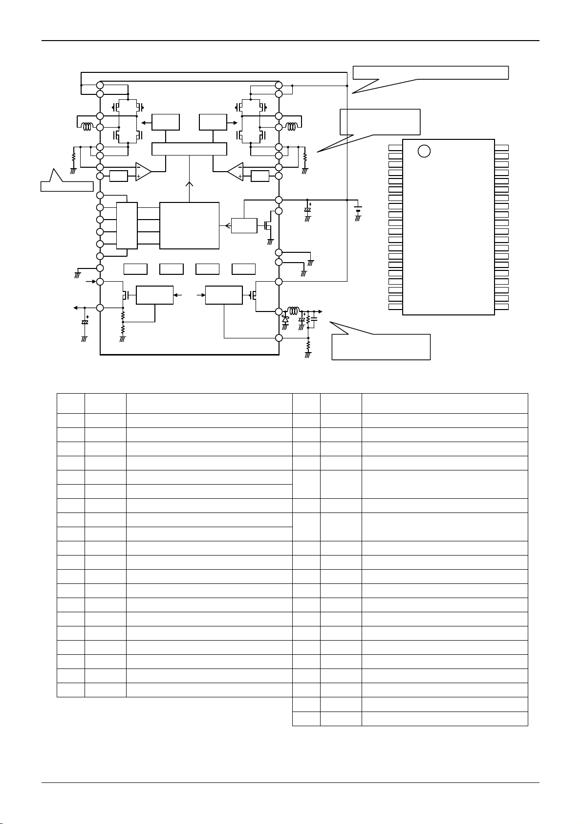
●Block Diagram, Application Circuit Diagram, and Pin Function
0.2Ω
(0.04~0.35Ω)
Same as RNF1
STROBE(DC1E
From
VDCDCOUT
(0.1µF~2.2µF)
VM2
VM2
OUT2P
OUT2M
RNF2
RNF2
RNF2S
VREF2
SELECT
DC2P
SCLK(DC1P)
DC2E
SDAT
GND
RIN
ROUT
1µF
VM1
1/10
8
9
7
2
3
4
5
20
31
28
40
21
10
12
18
VM1
OUT1P
OUT1M
RNF1
RNF1
RNF1S
VREF1
VM3
RESET
PGND
DGND
VM4
SWOUT
220µH
100µF
DSEN
0.2Ω
(0.04Ω~0.35Ω)
300µF
(220µF~470µF)
VDCDCOUT
2.7kΩ
4700pF
1kΩ
32
33
39
34
37
38
36
1/10
19
22
24
27
Selector
23
25
)
26
29
16
14
Pre
driver
CONTROL LOGIC
Serial
Control
BG BG
Pre
driver
POWER
MONITOR
RESET
BGTSD UVLOOSC
DRIVER REG
Be sure to use VM1,VM2.VM3 and VM4 by short-circuit.
0.2Ω(0.04Ω~0.35Ω)
Io1=(VREF1/10)・(1/RNF1S)
See P.9.
N.C.
1
OUT1M
2
RNF1
3
RNF1
4
RNF1S
5
N.C.
6
OUT1P
7
8
VM1
VM1
9
VM4
10
N.C.
11
SWOUT
12
N.C.
13
ROUT
14
N.C.
15
RIN
16
N.C.
17
DSEN
18
VREF2
19
VREF1
20
The figure on the left-hand side shows
optimum recommended values.
See P.10 for setting.
40
39
38
37
36
35
34
33
32
31
30
29
28
27
26
25
24
23
22
21
Fig.12 Block Diagram and Application Circuit Diagram Fig.13 Pin Assignment Diagram
No.
Pin
name
Function No.
Pin
name
Function
1 NC Non Connection 21 DGND Digital GND
2 OUT1M H-bridge output pin 1M 22 SELECT Input pin select pin
3 RNF1 Output current detection pin 1 23 DC2E H-bridge 2 side enable input pin
4 RNF1 Output current detection pin 1 24 DC2P H-bridge 2 side phase pin
5 RNF1S Output current detection input pin
6 NC Non Connection
25 STROBE
Serial port strobe input pin /
H-bridge 1 side enable pin
7 OUT1P H-bridge output pin 1P 26 SDATA Serial port data input pin
8 VM1 Motor power supply pin
9 VM1 Motor power supply pin
27 SCLK
Serial port clock input pin /
H-bridge 1 side phase input pin
10 VM4 Switching regulator power supply pin 28 RESET Reset signal output pin
11 NC Non Connection 29 AGND ANALOG GND
12 SWOUT Switching regulator output pin 30 NC Non Connection
13 NC Non Connection 31 VM3 Power supply pin
14 ROUT Series regulator output pin 32 VM2 Motor power supply pin
15 NC Non Connection 33 VM2 Motor power supply pin
16 RIN Series regulator power supply pin 34 OUT2M H-bridge output pin 2M
17 NC Non Connection 35 NC Non Connection
18 DSEN Switching regulator voltage sense pin 36 RNF2S Output current detection input pin
19 VREF2 Reference voltage input pin 37 RNF2 Output current detection pin 2
20 VREF1 Reference voltage input pin 38 RNF2 Output current detection pin 2
39 OUT2P H-bridge output pin 2P
40 PGND POWER GND
* Precaution regarding VM pin
If you use VM1, VM2, VM3 and VM4 not by short-circuit, they may be destroyed. Be sure to use them by short-circuit.
And be sure to set up a bypass capacitor (220µF to 470µF) closer to VM3 pin as much as possible.
PGND
OUT2P
RNF2
RNF2
RNF2S
N.C.
OUT2M
VM2
VM2
VM3
N.C.
AGND
RESET
SCLK
SDATA
STROBE
DC2P
DC2E
SELECT
DGND
www.rohm.com
© 2010 ROHM Co., Ltd. All rights reserved.
4/16
2010.06 - Rev.
Page 5

BD64550EFV
A
●Pin selection function
Either serial control or external PWM control can be selected for motor control type with SELECT pin (pin 22).
SELECT Output state
L Serial input mode
H External PWM control mode
STROBE/DC1E(25pin)
SDATA(26pin)
SCLK/DC1P(27pin)
DC2P(24pin)
DC2E(23pin)
ENA PHA
Internal shift register
SEL
SEL
Serial
SEL
Serial
SEL
Serial
SELECT(22pin)
Fig.14 Serial Input Block Diagram
The input/output logic at SELECT = H is as follows.
DC1E/DC2E Output state
L Open
H ACTIVE
DC1P/DC2P OUTP OUTM
L SINK SOURCE
H SOURCE SINK
○Procedure of DC motor drive by external PWM control
1) Serial setting
Set the serial by SELECT pin = L. (WORD_S and WORD_D setting)
・WORD_S (see P.7) is a drive parameter for setting OFF_TIME, BLANK TIME etc.
・WORD_D (see P.7) is for drive setting to set drive mode of each H-bridge.
When setting WORD_D (see P.7), make sure that ENABLE signal (ENABLE_1、ENABLE_2) of serial bit is L.
If ENABLE signal is H, the motor may operate.
Input of DC2P pin can be either H or L.
2) External PWM drive mode switch
Set external PWM drive mode by SELECT pin = H.
Switch by DC1E (STROBE)/CD2E pin = L when switching SELECT pin.
3) Drive
PHASE, ENABLE pin input signal (DC1E/DC1P/DC2E/DC2P) drives in external PWM mode.
Technical Note
OUTPUT
Control
Logic
www.rohm.com
© 2010 ROHM Co., Ltd. All rights reserved.
5/16
2010.06 - Rev.
Page 6

BD64550EFV
A
A
Technical Note
●Serial interface
16-bit 3-linear type serial interface (SDATA (pin 26), SCLK (pin 27), STROBE (pin 25)) is provided to set the operation and
the value of current limit. Data are sent to the internal shift register by falling edge of SCLK pin in the area L of STROBE pin.
Data of shift register are written in an appropriate address of internal memory of 2*15 bits by rising edge of STROBE pin
according to address data of D15.The input order of serial data is from D0 to D15.
Address data
D15 Word select
0 WORD_S
1 WORD_D
Memory data allocation
BIT WORD_S Default WORD_D Default
D0 Rohm_Reserve[2] 0 Rohm_Reserve[11] 0
D1 Rohm_Reserve[1] 0 Rohm_Reserve[10] 0
D2 Rohm_Reserve[0] 0 Rohm_Reserve[9] 0
D3 OFF TIME_2[2] 0 Rohm_Reserve[8] 0
D4 OFF TIME_2[1] 0 Rohm_Reserve[7] 0
D5 OFF TIME_2[0] 0 Rohm_Reserve[6] 0
D6 BLANK TIME_2[1] 0 Rohm_Reserve[5] 0
D7 BLANK TIME_2[0] 0 Rohm_Reserve[4] 0
D8 OFF TIME_1[2] 0 Rohm_Reserve[3] 0
D9 OFF TIME_1[1] 0 PWM_MODE_2 0
D10 OFF TIME_1[0] 0 S_PHASE_2 0
D11 BLANK TIME_1[1] 0 S_ENABLE_2 0
D12 BLANK TIME_1[0] 0 PWM_MODE_1 0
D13 MASK SELECT 0 S_PHASE_1 0
D14 SWOFF 0 S_ENABLE_1 0
The timing of serial report writing is shown in the right figure.
And the minimum timing of each is as follows:
A:SDATA setup time・・・・・・・・・・・・・・・・・・・ 10nsec
B:SDATA hold time・・・・・・・・・・・・・・・・・・・・ 10nsec
C:Setup STROBE to SCLK falling edge・・ 50nsec
D:SCLK low pulse width・・・・・・・・・・・・・・・・ 25nsec
E:SCLK High pulse width・・・・・・・・・・・・・・・ 25nsec
F:Setup SCLK falling edge to STROBE・・・ 25nsec
G:STROBE pulse width・・・・・・・・・・・・・・・・ 50nsec
H:Setup RESET to SCLK Rising・・・・・・・・・ 50µsec
H
RESET
STROBE
SCLK
B
D0
D1
D15
CGF E D
○RESET signal is an internal RESET signal and generated inside IC at the same timing of external RESET output.
○STROBE, SCLK and SDATA signals are input signals through external ASIC.
Fig.15 Serial Signal Input Timing
www.rohm.com
© 2010 ROHM Co., Ltd. All rights reserved.
6/16
2010.06 - Rev.
Page 7

BD64550EFV
A
●Serial Port Explanation
WORD_S
○SWOFF
Set on/off of switching regulator circuit.
○MASK SELECT
Common mask can be provided to 2-phase H-bridge drive noise mask (BLANK time).
○BLANK TIME
Current-limit comparator monitors RNF pin voltage to set limit to current, but during the period from switching on to BLANK
TIME, detection becomes invalid in order to avoid wrong detection caused by spike noise that happens at the time of
switching on. See P.8 for details.And during the period from ENABLE signal on to BLANK TIME at switching of PHASE
signal, detection becomes invalid as well.
○OFF TIME
Set current decay time.
WORD_D
○S_ENABLE_1/S_ENABLE_2
Each bridge on/off signal. Output state is as follows.
○S_PHASE_1/S_PHASE_2
Set the direction of current of each bridge. Output state is as follows.
○PWM_MODE_1/PWM_MODE_2
Set current decay mode in bridge1 and 2. (See page 8 for details about each mode.)
(※)Rohm_Reserve
0 Switching regulator on
1 Switching regulator off
0 Independent mask on single-phase/two-phase.
1 Common mask on single-phase/two-phase.
[1] [0] BLANK TIME Unit
0 0 2.0 µs
0 1 3.0 µs
1 0 4.0 µs
1 1 5.0 µs
[2] [1] [0] OFF TIME Unit
0 0 0 6 µs
0 0 1 8 µs
0 1 0 10 µs
0 1 1 12 µs
1 0 0 14 µs
1 0 1 16 µs
1 1 0 18 µs
1 1 1 20 µs
Output state
0 Open
1 ACTIVE
P M
0 SINK SOURCE
1 SOURCE SINK
0 FAST DECAY
1 SLOW DECAY
Rohm_Reserve is special mode setting port for inspection at shipment. Especially, if Rohm Reserve [3], [4], [5], [7], [8], [9], [10], [11] is set to H by mistake,
malfunction may be caused. Be sure not to set.
Technical Note
www.rohm.com
© 2010 ROHM Co., Ltd. All rights reserved.
7/16
2010.06 - Rev.
Page 8

BD64550EFV
A
Technical Note
●H-bridge Driver Operation
This IC has built-in 2-channel H-bridge driver.
Each can be used for DC motor drive independently.
1. Current setting
Motor output current-limit value can be set according to the equation below.
Io=(VREF/10)・(1/RNFS) [A]
Decide within the range VREF = 0.8V to 3.5V, RNFS = 0.04Ωto 0.35Ω.
2. DECAY mode
Current decay mode can be selected from serial input at the time of motor chopping drive.
Each mode and timing is as follows.
○SLOW DECAY mode ○FAST DECAY Mode ○Timing chart
VM
VM
ON→OFF
OFF→OFF
ON→OFF
OFF→OFF
(Internal 8 MHz)
Limit value
Output current
0 1
F
BASE
OFF→OFF
ON→ON
At the time on
At the time off (at DECAY)
OFF→OFF
At the time on
At the time off (at DECAY)
ON→OFF
On time
Off time
(Set by off time)
SLOW
FAST
Fig.16 On/Off Timing at SLOW Fig.17 On/Off Timing at FAST Fig.18 DECAY Mode Timing Chart
3. Protection area for output current value wrong detection
In order to avoid wrong detection of current detection comparator by varistor current element in each motor, current
detection are masked at the timing as follows.
①PHASE switching time
②ENABLE on time
③When output is on after OFF_TIME is finished at the time of current chopping drive
①PHASE switching time
PHASE signal
Motor current
Mask area
BLANK TIME
②ENABLE on time
Fig.19 Timing Chart of PHASE Switching Time
③Current chopping driving time
ENABLE
Motor current
Mask area
BLANK TIME
Fig.20 Timing Chart of ENABLE On Timing Fig.21 Timing Chart of Current Chopping Driving Time
RNF voltage
Mask area
BLANK TIME
OFF TIME
48
www.rohm.com
© 2010 ROHM Co., Ltd. All rights reserved.
8/16
2010.06 - Rev.
Page 9
BD64550EFV
A
Technical Note
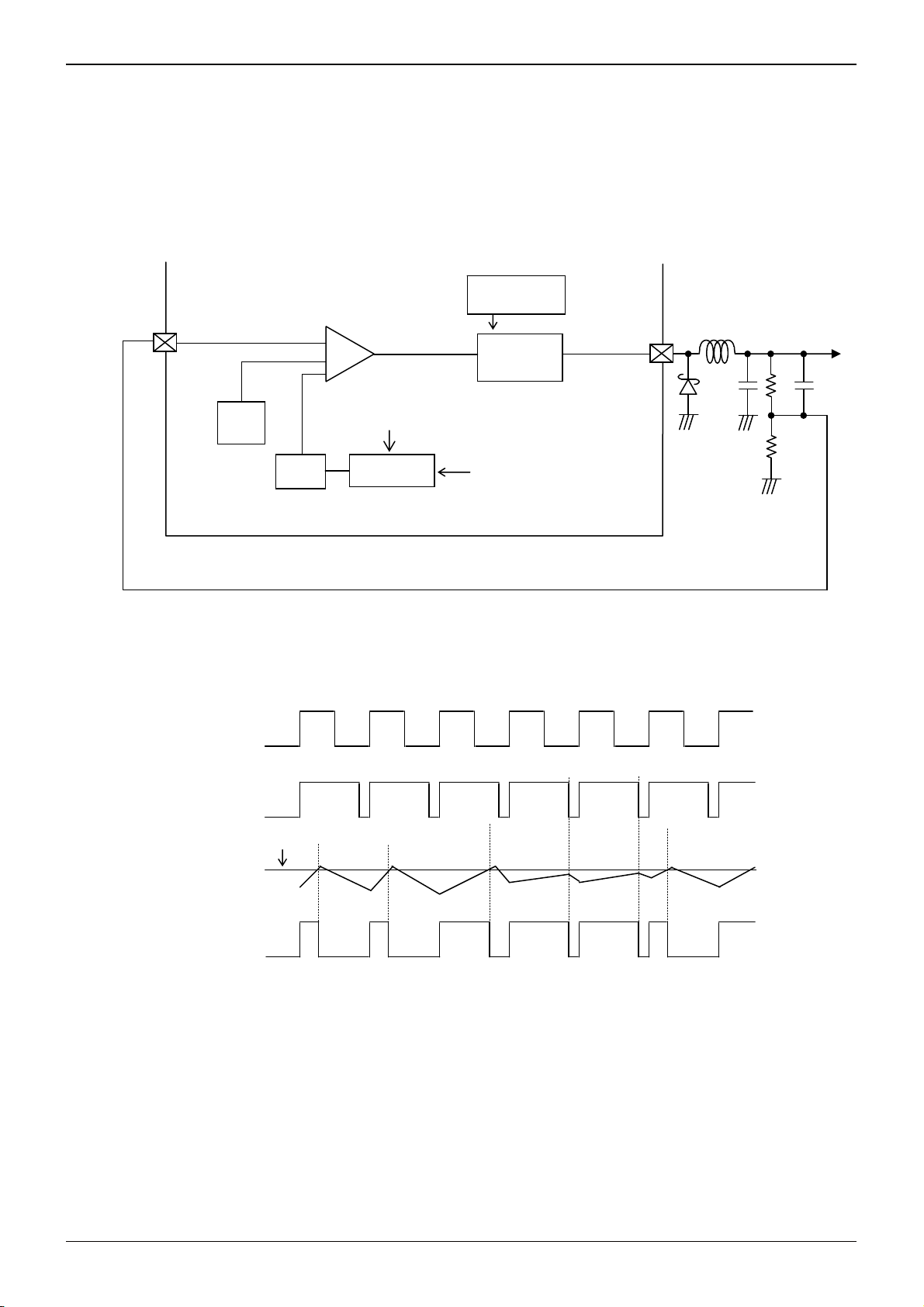
●Switching regulator operation
○Basic operation
A switching regulator circuit that repeats on/off being synchronized with internal CLK (200 KHz) is built-in.
The start up output voltage SWOUT (pin 12) becomes up and run step by step with soft start at the VM power-on
(VM≧V
).The output voltage is determined by the equation below with external resistance.
MPORH
VOUTDCDC=VBIAS・{(R1+R2)/R2 } [V]
The setting should be performed so that the switching regulator output voltage (VOUTDCDC) waveform is optimized within
the range of VOUTDCDC = 3V to 5V, VBIAS = 0.9V (Typ.), R1 + R2 = 1kΩ to 10kΩ, C1 = 1,000pF to 10,000pF.
DSEN
-
+
+
200KHzCLK
SWOUT
DRIVER
0.9V
BIAS
DAC
SWOFF
SS
COUNTER
CLK(=1.95kHz)
Fig.22 Switching Regulator Block Diagram
Reference clock
(200kHz)
DUTY MAX
Output voltage
MAX_DUTY 92%
⇒
SWOUT
Fig.23 Timing Chart of Switching Regulator Operation
VOUTDCDC
R1
DSEN
R2
C1
www.rohm.com
© 2010 ROHM Co., Ltd. All rights reserved.
9/16
2010.06 - Rev.
Page 10
BD64550EFV
A
Technical Note
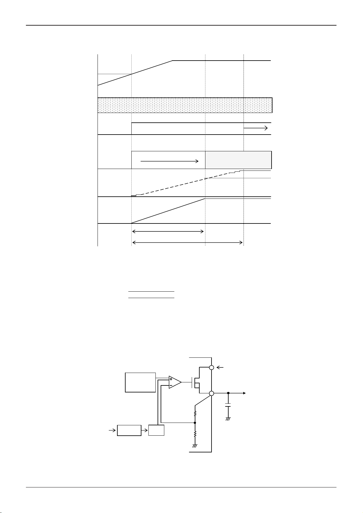
○Soft start
As shown in Fig.24, VOUTDCDC output voltage becomes up and run step by step with soft start at the time of power-on.
VM voltage
V
MPORH
CLK195
(Internal)
Oscillation
Counter output
1 2 3 4 5
・・ ・・・・・49・・・ ・・63 64
SWOUT
DAC output
VOUTDCDC output voltage
~Duty increase~
T1=23.6[msec]
T2=32.8[msec]
Constant ON Duty
ON Duty=
V
DCOUT
/VM
1.21V
0.90V
0V
5.0Vor3.3V
0V
Fig.24 Soft Starting Time Timing Chart
This soft start method is realized by changing comparator positive side voltage that determines output duty of switching
regulator to linear using DAC.
Soft start time T1 is constant value regardless of VM voltage.
Soft start time T1=23.6msec(typ.)
Count finish time T2=32.8msec(typ.)
○Series regulator operation
Inputting switching regulator output into RIN pin (pin 16) enables to drive series regulator circuit.
At the time of power-on, output voltage start up step by step with soft starting at the same timing as switching regulator
circuit.^Soft start time is 23.6ms (Typ.).
Regarding external capacitor of ROUT pin (pin 14), it works normally without setting. But switching noise of switching
regulator becomes easy to get in due to dragging on board pattern and the like. Pay attention to switching noise.
Regulator
0.9V
RIN
Switching regulator
ROUT
Internal CLK
1.95kHz
SS
COUNTER
DAC
20kΩ
(typ.)
30kΩ
(typ.)
Fig.25 Series Regulator Block Diagram
www.rohm.com
© 2010 ROHM Co., Ltd. All rights reserved.
10/16
2010.06 - Rev.
Page 11

BD64550EFV
A
●Protection function
○Protection circuit function
Overall Overheating protection
DC motor drive circuit Overcurrent protection
Switching regulator circuit Overcurrent protection, output overvoltage protection, output low voltage protection
Series regulator circuit None
○Operation at protection circuit operation
①Overheating protection・・・All functions are shutout along with junction temperature rise
Thermal shutdown temperature 175℃(typ.)
Switching regulator Series regulator DC motor RESET Re-start
At protection operation OFF OFF OFF L Again power-on
②Overcurrent protection (Switching regulator)
Set current Mask time State after operation
I
2.6(A) 0.5µsec
SWOC
(※)
All function shutout
Switching regulator Series regulator DC motor RESET Re-start
Operating OFF OFF OFF L Again power-on
③Overcurrent protection (DC motor)
Set current Mask time State after operation
I
3.8(A) 1.5µsec Shown below
DCOC
Switching regulator Series regulator DC motor RESET Re-start
Operating ON ON OFF L_PULSE Serial re-input
Motor current
IDCOC setting value
RESET signal
L
Serial data
Data default
1.5μsec
40msec
Fig.26 Timing Chart of Motor Overcurrent Protection
(※) If the output pulse of switching regulator is 0.5µs or below, the overcurrent function does not operate even at the time of overcurrent outflow.
Technical Note
www.rohm.com
© 2010 ROHM Co., Ltd. All rights reserved.
11/16
2010.06 - Rev.
Page 12
BD64550EFV
A
Technical Note
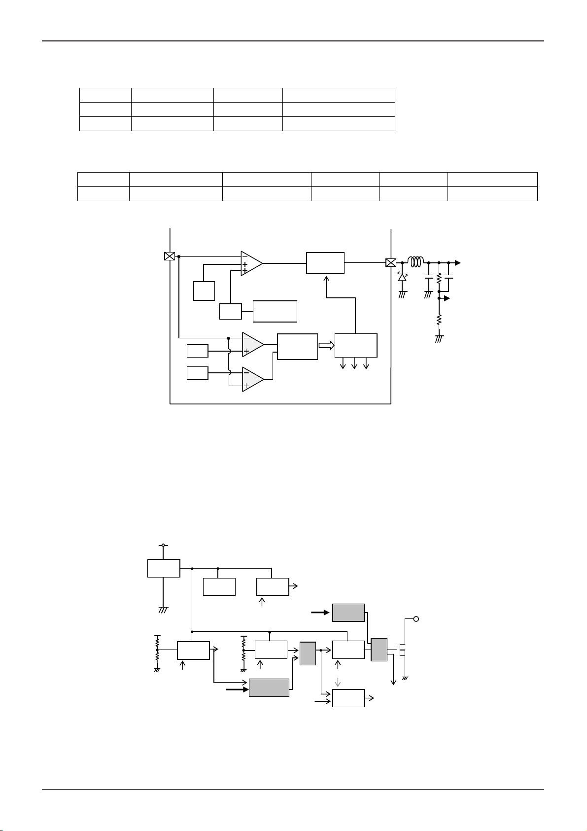
④Low voltage protection/overvoltage protection circuit
All functions are shutout on the condition of setting value (+30%, -30%) while DSEN pin voltage (pin 18) of switching
regulator circuit is monitored.
Set voltage Mask time State after operation
VSWLV 0.60(V) 10µsec All function shutout
VSWOH 1.20(V) 10µsec All function shutout
Note that output overvoltage and output low voltage protection does not work until soft start count finish (32.8 ms, Typ.)
at the time of start up of DC/DC power after power-on.
Switching regulator Series regulator DC motor RESET Re-start
Operating OFF OFF OFF L Again power-on
DSEN
0.9V
BIAS
SWOUT
DRIVER
DAC
SS
COUNTER
DSEN
0.60V
1.21V
Mask during
soft starting
All function
off circuit
Fig.27 Switching Regulator Block Diagram
○RESET function
Power-on RESET circuit is built-in for VM power source.
H is output at RESET pin through DELAY time of internal counter when power voltage goes up to V
(6.5 V, Typ.) or
MPORH
higher at the time of power-on. In addition, hysteresis is set up at the time of power-down to output L at RESET pin with
VMPORL (6.1 V, Typ.) And no response time (2.5µs, Typ.) of voltage detection is set in order to avoid wrong detection by
sudden power-off.If protection circuits other than overcurrent protection of motor starts operating, RESET is not released if
VM power is not on again.
VM
Internal
regulator
B.G
VM
UVLO
BG
Protection detection other than
DCOC
RESET1
VM
OSC
RESET1
POWER
monitor
BG
Latch circuit
DCOC
AND
SWOFF
RESET2
DCOC
Counter
POR
Counter
OSC
Counter
SS
AND
(SOFT START)
RESET
Fig.28 RESET Internal Circuit Block Diagram
www.rohm.com
© 2010 ROHM Co., Ltd. All rights reserved.
12/16
2010.06 - Rev.
Page 13
BD64550EFV
A
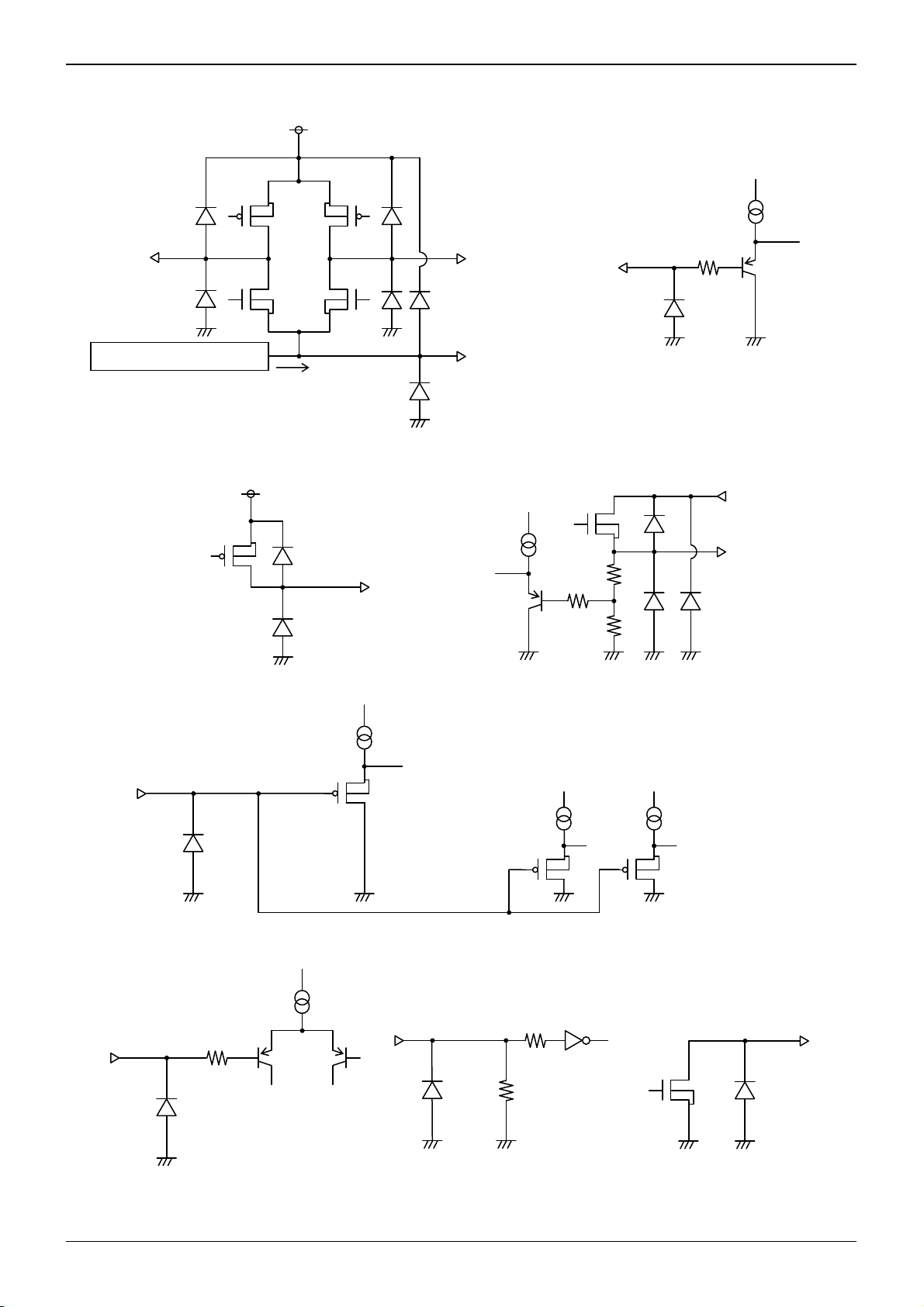
●I/O Circuit Diagram
① OUT1P, OUT1M, OUT2P, OUT2M, RNF1 and RNF2 ② RNF1S and RNF2S
VM1, VM2
OUT1P, OUT2P
OUT1M, OUT2M
RNF1S, RNF2S
Overcurrent protection circuit
15μA(TYP.)
RNF1, RNF2
③ SWOUT ④ RIN and ROUT
VM4
SWOUT
⑤ DSEN
DSEN
⑥ VREF1 and VREF2 ⑦ Logic input ⑧ RESET
Fig.29 I/O Circuit
Technical Note
RIN
ROUT
RESET
www.rohm.com
© 2010 ROHM Co., Ltd. All rights reserved.
13/16
2010.06 - Rev.
Page 14

BD64550EFV
A
Technical Note
●Power Dissipation Reduction
On the backside of HTSSOP-B40 package, metal is filled in. Heat dissipation is possible by letting in a through hole from
backside. Power dissipation can be improved by providing heat dissipation pattern of copper foil or the like not only on the
board surface but also on the backside. The metal on the backside shorts with the backside of IC tip and the potential is GND.
Therefore, avoid shorts with other potential than GND, or malfunction or destruction may happen. It is recommended that
backside metal should short with GND by soldering.
W)
(
Pd
:
5.0
4.5
4.0
3.5
3.0
2.5
2.0
1.5
④4.7W
③3.6W
1.95W
②
1.6W
①
Measuring instrument: TH156 (Kuwano Denki)
Measuring state: ROHM substrate mounted
Board size:70mm×70mm×1.6mm(Thermal via on the board)
Solder the board and exposed heat release part of package backside.
Board①:1-layer board (Backside copper foil area: 0 mm x 0 mm)
Board②:2-layer board (Backside copper foil area: 15 mm x 15 mm)
Board③:2-layer board (Backside copper foil area: 15 mm x 15 mm)
Board④:4-layer board (Backside copper foil area: 70 mm x 70 mm)
Board①:θja=78.1℃/W
Board②:θja= 64.1℃/W
Board③:θja=34.7℃/W
Board④:θja=26.6℃/W
Power Dissipation
1.0
0.5
0.0
0 25 50 75 100 125 150 175
Ambient Temperature : Ta(℃)
Fig.30 Power Dissipation Reduction
●Notes for Use
1) Absolute maximum ratings
Use of the IC in excess of absolute maximum ratings such as the applied voltage or operating temperature range may
result in IC damage. Assumptions should not be made regarding the state of the IC (short mode or open mode) when such
damage is suffered. A physical safety measure such as a fuse should be implemented when use of the IC in a special
mode where the absolute maximum ratings may be exceeded is anticipated.
2) Connecting the power supply connector backward
Connecting the power supply connector backwards may result in damage to the IC. Insert external diodes between the power
supply and the IC's power supply pins as well as the motor coil to protect against damage from backward connections.
3) Power supply lines
As return of current regenerated by back EMF of motor happens, take steps such as putting capacitor between power
supply and GND as a electric pathway for the regenerated current. Be sure that there is no problem with each property
such as emptied capacity at lower temperature regarding electrolytic capacitor to decide capacity value.
If the connected power supply does not have sufficient current absorption capacity, regenerative current will cause the
voltage on the power supply line to rise, which combined with the product and its peripheral circuitry may exceed the
absolute maximum ratings. It is recommended to implement a physical safety measure such as the insertion of a voltage
clamp diode between the power supply and GND pins.
4) GND potential
Ensure a minimum GND pin potential in all operating conditions.
www.rohm.com
© 2010 ROHM Co., Ltd. All rights reserved.
14/16
2010.06 - Rev.
Page 15

BD64550EFV
A
P
iti
P
iti
Technical Note
5) Setting of heat
Use a thermal design that allows for a sufficient margin in light of the power dissipation (Pd) in actual operating conditions.
BD64550EFV expose its frame of the backside of package. Note that this part is assumed to use after providing heat
dissipation treatment to improve heat dissipation efficiency . Try to occupy as wide as possible with heat dissipation
pattern not only on the board surface but also the backside.
6) Pin short and mistake fitting
Use caution when orienting and positioning the IC for mounting on printed circuit boards. Improper mounting may result in
damage to the IC. Shorts between output pins or between output pins and the power supply and GND pins caused by the
presence of a foreign object may result in damage to the IC.
7) Actions in strong magnetic field
Use caution when using the IC in the presence of a strong magnetic field as doing so may cause the IC to malfunction.
8) ASO
When using the IC, set the output transistor so that it does not exceed absolute maximum ratings or ASO.
9) Thermal shutdown circuit
The IC has a built-in thermal shutdown circuit (TSD circuit). If the chip temperature becomes Tjmax=150℃, and higher,
coil output to the motor and regulator output will be OFF, and reset output will be L. The TSD circuit is designed only to
shut the IC off to prevent runaway thermal operation. It is not designed to protect or indemnify peripheral equipment. Do
not use the TSD function to protect peripheral equipment.
10) Testing on application boards
When testing the IC on an application board, connecting a capacitor to a pin with low impedance subjects the IC to stress.
Always discharge capacitors after each process or step. Ground the IC during assembly steps as an antistatic measure,
and use similar caution when transporting or storing the IC. Always turn the IC's power supply off before connecting it to or
removing it from a jig or fixture during the inspection process.
11) Regarding input pin of the IC
This monolithic IC contains P+ isolation and P substrate layers between adjacent elements in order to keep them
isolated/N junctions are formed at the intersection of these P layers with the N layers of other elements to create a variety
of parasitic elements. For example, when a resistor and transistor are connected to pins as shown in Fig. 31,
○the P/N junction functions as a parasitic diode
when GND > (Pin A) for the resistor or GND > (Pin B) for the transistor (NPN).
○Similarly, when GND > (Pin B) for the transistor (NPN), the parasitic diode described above combines
with the N layer of other adjacent elements to operate as a parasitic NPN transistor.
The formation of parasitic elements as a result of the relationships of the potentials of different pins is an inevitable result of the
IC's architecture. The operation of parasitic elements can cause interference with circuit operation as well as IC malfunction and
damage. For these reasons, it is necessary to use caution so that the IC is not used in a way that will trigger the operation of
parasitic elements, such as by the application of voltages lower than the GND (P substrate) voltage to input pins.
Pin A
+
N
P
P
P
Parasitic element
GND
Resistor
+
N N
P substrate
Pin B
Pin A
aras
element
Fig.31 example of IC structure
N
c
Parasitic element
Tr
B
C
+
P
E
N
P
GND
+
P
N
P substrate
GND
Pin B
B C
E
GND
Other adjacent elements
12) Ground Wiring Pattern
When using both small signal and large current GND patterns, it is recommended to isolate the two ground patterns,
placing a single ground point at the application's reference point so that the pattern wiring resistance and voltage
variations caused by large currents do not cause variations in the small signal ground voltage. Be careful not to change the
GND wiring pattern of any external components, either.
aras
element
c
www.rohm.com
© 2010 ROHM Co., Ltd. All rights reserved.
15/16
2010.06 - Rev.
Page 16

BD64550EFV
A
●Ordering Part Number
B D 6 4 5 5 0 E F V - E 2
Technical Note
Part No. Part No.
HTSSOP-B40
(MAX 13.95 include BURR)
5.4±0.1
7.8±0.2
1
0.08±0.05
1PIN MARK
0.65
0.625
1.0Max.
0.85±0.05
13.6±0.1
(8.4)
0.08 S
0.24
Package
EFV : HTSSOP-B40
Packaging and forming specification
E2: Embossed tape and reel
<Tape and Reel information>
+6
4
−4
2140
(3.2)
20
+0.05
−0.04
0.17
S
0.08
1.2 ± 0.2
0.5 ± 0.15
+0.05
−0.03
M
(Unit : mm)
Quantity
Direction
of feed
Embossed carrier tape (with dry pack)Tape
2000pcs
E2
The direction is the 1pin of product is at the upper left when you hold
()
reel on the left hand and you pull out the tape on the right hand
Direction of feed
Reel
1pin
Order quantity needs to be multiple of the minimum quantity.
∗
www.rohm.com
© 2010 ROHM Co., Ltd. All rights reserved.
16/16
2010.06 - Rev.
Page 17

Notes
No copying or reproduction of this document, in part or in whole, is permitted without the
consent of ROHM Co.,Ltd.
The content specied herein is subject to change for improvement without notice.
The content specied herein is for the purpose of introducing ROHM's products (hereinaf ter
"Products"). If you wish to use any such Product, please be sure to refer to the specications,
which can be obtained from ROHM upon request.
Examples of application circuits, circuit constants and any other information contained herein
illustrate the standard usage and operations of the Products. The peripheral conditions must
be taken into account when designing circuits for mass production.
Great care was taken in ensuring the accuracy of the information specied in this document.
However, should you incur any damage arising from any inaccuracy or misprint of such
information, ROHM shall bear no responsibility for such damage.
The technical information specied herein is intended only to show the typical functions of and
examples of application circuits for the Products. ROHM does not grant you, explicitly or
implicitly, any license to use or exercise intellectual property or other rights held by ROHM and
other parties. ROHM shall bear no responsibility whatsoever for any dispute arising from the
use of such technical information.
Notice
The Products specied in this document are intended to be used with general-use electronic
equipment or devices (such as audio visual equipment, ofce-automation equipment, communication devices, electronic appliances and amusement devices).
The Products specied in this document are not designed to be radiation tolerant.
While ROHM always makes effor ts to enhance the quality and reliability of its Products, a
Product may fail or malfunction for a variety of reasons.
Please be sure to implement in your equipment using the Products safety measures to guard
against the possibility of physical injur y, re or any other damage caused in the event of the
failure of any Product, such as derating, redundancy, re control and fail-safe designs. ROHM
shall bear no responsibility whatsoever for your use of any Product outside of the prescribed
scope or not in accordance with the instruction manual.
The Products are not designed or manufactured to be used with any equipment, device or
system which requires an extremely high level of reliability the failure or malfunction of which
may result in a direct threat to human life or create a risk of human injury (such as a medical
instrument, transportation equipment, aerospace machinery, nuclear-reactor controller, fuelcontroller or other safety device). ROHM shall bear no responsibility in any way for use of any
of the Products for the above special purposes. If a Product is intended to be used for any
such special purpose, please contact a ROHM sales representative before purchasing.
If you intend to export or ship overseas any Product or technology specied herein that may
be controlled under the Foreign Exchange and the Foreign Trade Law, you will be required to
obtain a license or permit under the Law.
Thank you for your accessing to ROHM product informations.
More detail product informations and catalogs are available, please contact us.
ROHM Customer Support System
www.rohm.com
© 2010 ROHM Co., Ltd. All rights reserved.
http://www.rohm.com/contact/
R1010
A
 Loading...