

A
Stepping Motor Driver series
High Voltage Series
Stepping Motor Drivers
BD6422EFV (PARALLEL-IN type)
BD6425, BD6423EFV (CLK-IN type)
●Description
These products are a low power consumption PWM constant current-drive driver of bipolar stepping motor with power
supply’s rated voltage of 45V and rated output current of 1.0A, 1.5A.
●Feature
1) Power supply: one system drive (rated voltage of 45V)
2) Rated output current: 1.0A, 1.5A
3) Low ON resistance DMOS output
4) CLK-IN drive mode (BD6425/6423EFV)
5) Parallel IN drive mode (BD6422EFV)
6) PWM constant current control (other oscillation)
7) Built-in spike noise blanking function (external noise filter is unnecessary)
8) FULL STEP & HALF STEP (two kinds), applicable to QUARTER STEP
9) Current decay mode switching function (4 kinds of FAST/SLOW DECAY ratio)
10) Normal rotation & reverse rotation switching function (BD6425/6423EFV)
11) Power save function
12) Built-in logic input pull-down resistor
13) Power-on reset function(BD6425/6423EFV)
14) Thermal shutdown circuit (TSD)
15) Over current protection circuit (OCP)
16) Under voltage lock out circuit (UVLO)
17) Malfunction prevention at the time of no applied power supply (Ghost Supply Prevention)
18) Electrostatic discharge: 8kV (HBM specification)
19) Microminiature, ultra-thin and high heat-radiation (exposed metal type) HTSSOP package
●Application
serial dot impact printer、sewing machine etc.
●Absolute maximum ratings(Ta=25℃)
Item Symbol BD6425EFV BD6423/6422EFV Unit
Supply voltage V
Power dissipation Pd
Input voltage for control pin VIN -0.2~+5.5 -0.2~+5.5 V
RNF maximum voltage V
Maximum output current I
Operating temperature range T
Storage temperature range T
Junction temperature T
※1 70mm×70mm×1.6mm glass epoxy board. Derating in done at 11.6mW/℃ for operating above Ta=25℃.
※2 4-layer recommended board. Derating in done at 37.6mW/℃ for operating above Ta=25℃.
※3 70mm×70mm×1.6mm glass epoxy board. Derating in done at 8.8mW/℃ for operating above Ta=25℃.
※4 4-layer recommended board. Derating in done at 32.0mW/℃ for operating above Ta=25℃.
※5 Do not, however exceed Pd, ASO and Tjmax=150℃.
-0.2~+45.0 -0.2~+45.0 V
CC1,2
0.7 0.7 V
RNF
1.5
OUT
-25~+85 -25~+85 ℃
opr
-55~+150 -55~+150 ℃
stg
+150 +150 ℃
jmax
1
※
1.45
1.1
2
※
4.70
4.0
5
※
1.0
3
※
4
※
5
※
A/phase
No.12009EAT06
W
W
www.rohm.com
© 2012 ROHM Co., Ltd. All rights reserved.
1/8
2012.02 - Rev.
BD6422EFV, BD6423EFV, BD6425EFV
A
●Operating conditions( (Ta= -25~+85℃)
Item Symbol BD6425EFV BD6423/6422EFV Unit
Supply voltage V
Maximum Output current (DC) I
※6 Do not however exceed Pd, ASO.
19~42 V
CC1,2
1.2
OUT
6
※
0.7
●Electrical characteristics (Unless otherwise specified Ta=25℃、V
Item Symbol
Min. Typ. Max.
Whole
Circuit current at standby
Circuit current
I
CCST
ICC - 2.0 5.0 mA PS=H, VREF=3V
- 1.0 2.5 mA PS=L
Control input
V
H level input voltage
L level input voltage
H level input current
L level input current
2.0 - - V
INH
V
- - 0.8 V
INL
I
35 50 100 μAVIN=5V
INH
I
-10 0 - μAVIN=0V
INL
Output (OUT1A, OUT1B, OUT2A, OUT2B)
Output ON resistance(BD6425EFV)
Output ON resistance(BD6423/6422EFV)
Output leak current
RON - 1.10 1.43 Ω I
R
- 2.00 2.60 Ω I
ON
I
- - 10 μA
LEAK
Current control
RNFXS input current (BD6425EFV)
RNFX input current
VREF input current
VREF input voltage range
Minimum on time (Blank time)
I
RNFS
I
RNF
I
VREF
V
REF
t
ONMIN
-2.0 -0.1 - μA RNFXS=0V
-40 -20 - μA RNFX=0V
-2.0 -0.1 - μAVREF=0V
0 - 3.0 V
0.5 1.5 3.0 μs C=470pF, R=82kΩ
BD6425/6423EFV
Comparator threshold
V
CTH
0.57 0.60 0.63 V VREF=3V
BD6422EFV
Comparator threshold 100% V
Comparator threshold 67% V
Comparator threshold 33% V
CTH100
CTH67
CTH33
0.57 0.60 0.63 V VREF=3V, (I0X,I1X)=(L,L)
0.38 0.40 0.42 V VREF=3V, (I0X,I1X)=(H,L)
0.18 0.20 0.22 V VREF=3V, (I0X,I1X)=(L,H)
CC1,2
=37V)
Limit
6
※
A/phase
Unit Condition
=1.0A,Sum of upper and lower
OUT
=0.5A,Sum of upper and lower
OUT
Technical Note
www.rohm.com
© 2012 ROHM Co., Ltd. All rights reserved.
2/8
2012.02 - Rev.
BD6422EFV, BD6423EFV, BD6425EFV
A
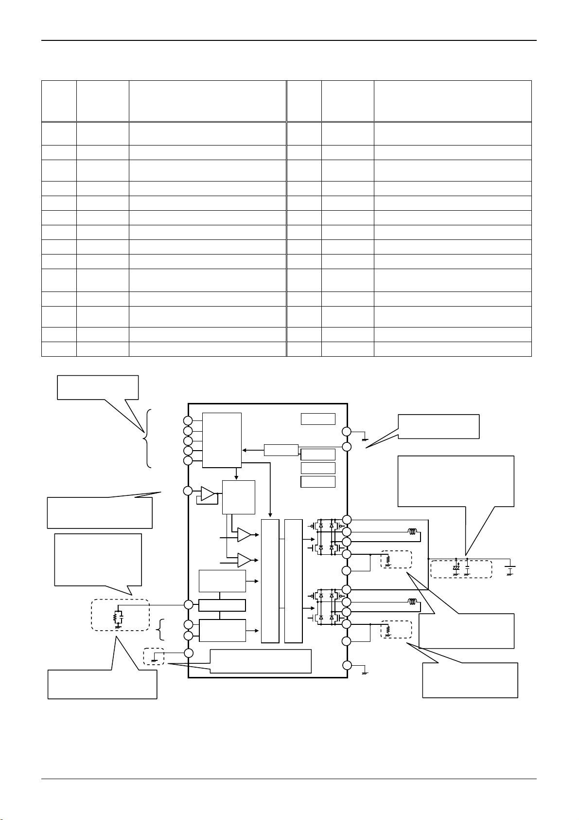
●Terminal function and Application circuit diagram
1) BD6425EFV
Pin
Pin name Function
No.
Technical Note
Pin
Pin name Function
No.
1 GND Ground terminal 15 CLK
Clock input terminal for advancing the
electrical angle.
2 OUT1B H bridge output terminal 16 CW_CCW Motor rotating direction setting terminal
3 RNF1
Connection terminal of resistor for output
current detection
17 TEST
Terminal for testing
(used by connecting with GND)
4 RNF1S Input terminal of current limit comparator 18 MODE0 Motor excitation mode setting terminal
5 OUT1A H bridge output terminal 19 MODE1 Motor excitation mode setting terminal
6 NC Non connection 20 ENABLE Power supply terminal
7 VCC1 Power supply terminal 21 NC Non connection
8 NC Non connection 22 VCC2 Power supply terminal
9 GND Ground terminal 23 NC Non connection
10 CR
Connection terminal of CR for setting
chopping frequency
24 OUT2A H bridge output terminal
11 DEC1 Current decay mode setting terminal 25 RNF2S Input terminal of current limit comparator
12 DEC2 Current decay mode setting terminal 26 RNF2
Connection terminal of resistor for output
current detection
13 VREF Output current value setting terminal 27 OUT2B H bridge output terminal
14 PS Power save terminal 28 NC Non connection
Logic input terminal.
Set the output currenet.
Input by resistor divison.
Set the chopping
frequency.
Setting range is
C:330pF~1500pF
R:15kΩ~200kΩ
82kΩ
Logic input terminal.
for setting current decay mode
470pF
CW_CCW
MODE1
ENABLE
VREF 13
CR
TEST
15 CLK
16
18 MODE0
19
20
10
11 DEC1
12 DEC2
17
Translator
+
-
RNF1
RNF2
Blank time
PWM control
Mix decay
2bit DAC
+
-
+
-
OSC
control
Terminal for testing.
Please connect to GND.
RESET
Control logic
Regulator
Predriver
UVLO
TSD
OCP
9
14
7
5
2
3
4
22
24
27
26
25
1
GND
PS
VCC1
OUT1A
OUT1B
RNF1
RNF1S
VCC2
OUT2A
OUT2B
RNF2
RNF1S
GND
Power save terminal.
Bypass capacitor.
Setting range is
100uF~470uF(electrolytic)
0.01uF~0.1uF(multilayer ceramic etc.)
Be sure to short VCC1 & VCC2.
0.3Ω
0.3Ω
100uF
Resistor for current. detecting.
Setting range is
0.2Ω~0.4Ω.
Resistor for current. detecting.
Setting range is
0.2Ω~0.4Ω.
0.1uF
Fig.1 Block diagram & Application circuit diagram of BD6425EFV
www.rohm.com
© 2012 ROHM Co., Ltd. All rights reserved.
3/8
2012.02 - Rev.

BD6422EFV, BD6423EFV, BD6425EFV
A
R
K
Technical Note
2) BD6423EFV
Pin
No.
Pin name Function
1 GND Ground terminal 13 CLK
Pin
No.
Pin name Function
Clock input terminal
for advancing the electrical angle.
2 OUT1B H bridge output terminal 14 CW_CCW Motor rotating direction setting terminal
3 RNF1
Connection terminal of resistor for output
current detection
15 TEST
Terminal for testing
(used by connecting with GND)
4 OUT1A H bridge output terminal 16 MODE0 Motor excitation mode setting terminal
5 VCC1 Power supply terminal 17 MODE1 Motor excitation mode setting terminal
6 NC Non connection 18 ENABLE Output enable terminal
7 GND Ground terminal 19 NC Non connection
8 CR
9 DEC1
10 DEC2
Connection terminal of CR for setting
PWM frequency
Current decay mode setting terminal
Current decay mode setting terminal
20 VCC2 Power supply terminal
21 OUT2A H bridge output terminal
22 RNF2
Connection terminal of resistor for output
current detection
11 VREF Output current value setting terminal 23 OUT2B H bridge output terminal
12 PS Power save terminal 24 NC Non connection
Logic input terminal
Setting output current
Input by resistance division.
Set the PWM frequency.
Setting range is
C:330pF~1500pF
R:15kΩ~200kΩ
Logic input terminal
for setting current decay mode
82kΩ
470pF
CW_CCW
MODE1
ENABLE
VREF 11
C
TEST
13 CL
14
16 MODE0
17
18
8
9 DEC1
10 DEC2
15
Translator
+
-
2bit DAC
RNF1
RNF2
Blank time
PWM control
OSC
Mix decay
control
Regulator
RESET
+
-
+
-
Control logic
UVLO
TSD
OCP
Predriver
7
12
5
4
2
3
20
21
23
22
1
GND
PS
VCC1
OUT1A
OUT1B
RNF1
VCC2
OUT2A
OUT2B
RNF2
GND
Power save terminal.
Bypass capacitor.
Setting range is
100uF~470uF(electrolytic)
0.01uF~0.1uF(multilayer ceramic etc.)
Be sure to short VCC1 & VCC2.
0.5Ω
100uF
Resistor for current. detecting.
0.5Ω
Setting range is
0.4Ω~0.8Ω.
Terminal for testing.
Please connect to GND.
Resistor for current. detecting.
Setting range is
0.4Ω~0.8Ω.
Fig.2 Block diagram & Application circuit diagram of BD6423EFV
0.1uF
www.rohm.com
© 2012 ROHM Co., Ltd. All rights reserved.
4/8
2012.02 - Rev.

BD6422EFV, BD6423EFV, BD6425EFV
A
equency
R
3) BD6422EFV
Pin
Pin name Function
No.
Technical Note
Pin
Pin name Function
No.
1 GND Ground terminal 13 PHASE1
Phase selection terminal
2 OUT1B H bridge output terminal 14 I01 VREF division ratio setting terminal
3 RNF1
Connection terminal of resistor for output
current detection
15 I11
VREF division ratio setting terminal
4 OUT1A H bridge output terminal 16 PHASE2 Phase selection terminal
5 VCC1 Power supply terminal 17 I02
6 NC Non connection 18 I12
VREF division ratio setting terminal
VREF division ratio setting terminal
7 GND Ground terminal 19 NC Non connection
8 CR
9 DEC1
10 DEC2
Connection terminal of CR for setting
PWM fr
Current decay mode setting terminal
Current decay mode setting terminal
20 VCC2
Power supply terminal
21 OUT2A H bridge output terminal
22 RNF2
Connection terminal of resistor for output
current detection
11 VREF Output current value setting terminal 23 OUT2B H bridge output terminal
12 PS Power save terminal 24 NC Non connection
Logic input terminal.
Setting output current.
Input by resistance division.
Set the PWM frequency.
Setting range is
C:330pF~1500pF
R:15kΩ~200kΩ
82kΩ
Logic input terminal.
for setting current decay mode
470pF
16 PHASE2
I01
I11
I02
I12
18
VREF 11
C
13 PHASE1
14
15
17
RNF1
RNF2
8
9 DEC1
10 DEC2
+
-
2bit DAC
Blank time
PWM control
OSC
Mix decay
control
Regulator
UVLO
TSD
+
-
+
-
Control Logic
OCP
Predriver
7
12
5
4
2
3
20
21
23
22
1
GND
PS
VCC1
OUT1A
OUT1B
RNF1
VCC2
OUT2A
OUT2B
RNF2
GND
Power save terminal.
Bypass capacitor.
Setting range is
100uF~470uF(electrolytic)
0.01uF~0.1uF(multilayer ceramic etc.)
Be sure to short VCC1 & VCC2.
0.5Ω
100uF
Resistor for current. detecting.
0.5Ω
Resistor for current. detecting.
Setting range is
0.4Ω~0.8Ω.
Setting range is
0.4Ω~1.0Ω.
Fig.3 Block diagram & Application circuit diagram of BD6422EFV
0.1uF
www.rohm.com
© 2012 ROHM Co., Ltd. All rights reserved.
5/8
2012.02 - Rev.

BD6422EFV, BD6423EFV, BD6425EFV
A
●Usage Notes
(1) Absolute maximum ratings
An excess in the absolute maximum ratings, such as supply voltage, temperature range of operating conditions, etc., can
break down the devices, thus making impossible to identify breaking mode, such as a short circuit or an open circuit. If
any over rated values will expect to exceed the absolute maximum ratings, consider adding circuit protection devices,
such as fuses.
(2) Connecting the power supply connector backward
Connecting of the power supply in reverse polarity can damage IC. Take precautions when connecting the power supply
lines. An external direction diode can be added.
(3) Power supply Lines
Design PCB layout pattern to provide low impedance GND and supply lines. To obtain a low noise ground and supply line,
separate the ground section and supply lines of the digital and analog blocks. Furthermore, for all power supply terminals
to ICs, connect a capacitor between the power supply and the GND terminal. When applying electrolytic capacitors in the
circuit, not that capacitance characteristic values are reduced at low temperatures.
(4) GND Potential
The potential of GND pin must be minimum potential in all operating conditions.
(5) Metal on the backside (Define the side where product markings are printed as front)
The metal on the backside is shorted with the backside of IC chip therefore it should be connected to GND. Be aware that
there is a possibility of malfunction or destruction if it is shorted with any potential other than GND.
(6) Thermal design
Use a thermal design that allows for a sufficient margin in light of the power dissipation (Pd) in actual operating conditions.
Users should be aware that these products have been designed to expose their frames at the back of the package, and
should be used with suitable heat dissipation treatment in this area to improve dissipation. As large a dissipation pattern
should be taken as possible, not only on the front of the baseboard but also on the back surface. It is important to
consider actual usage conditions and to take as large a dissipation pattern as possible.
(7) Inter-pin shorts and mounting errors
When attaching to a printed circuit board, pay close attention to the direction of the IC and displacement. Improper
attachment may lead to destruction of the IC. There is also possibility of destruction from short circuits which can be
caused by foreign matter entering between outputs or an output and the power supply or GND.
(8) Operation in a strong electric field
Use caution when using the IC in the presence of a strong electromagnetic field as doing so may cause the IC to
malfunction.
(9) ASO
When using the IC, set the output transistor so that it does not exceed absolute maximum ratings or ASO.
(10) Thermal shutdown circuit
The IC has a built-in thermal shutdown circuit (TSD circuit). If the chip temperature becomes Tjmax=150℃, and higher,
coil output to the motor will be open. The TSD circuit is designed only to shut the IC off to prevent runaway thermal
operation. It is not designed to protect or indemnify peripheral equipment. Do not use the TSD function to protect
peripheral equipment.
TSD on temperature [℃] (Typ.) Hysteresis Temperature [℃] (Typ.)
175 25
(11) Inspection of the application board
During inspection of the application board, if a capacitor is connected to a pin with low impedance there is a possibility
that it could cause stress to the IC, therefore an electrical discharge should be performed after each process. Also, as a
measure again electrostatic discharge, it should be earthed during the assembly process and special care should be
taken during transport or storage. Furthermore, when connecting to the jig during the inspection process, the power
supply should first be turned off and then removed before the inspection.
Technical Note
www.rohm.com
© 2012 ROHM Co., Ltd. All rights reserved.
6/8
2012.02 - Rev.

BD6422EFV, BD6423EFV, BD6425EFV
A
P
iti
P
iti
Technical Note
(12) Input terminal of IC
This IC is a monolithic IC, and between each element there is a P+ isolation for element partition and a P substrate.
This P layer and each element’s N layer make up the P-N junction, and various parasitic elements are made up.
For example, when the resistance and transistor are connected to the terminal as shown in figure 4,
○When GND>(Terminal A) at the resistance and GND>(Terminal B) at the transistor (NPN),
the P-N junction operates as a parasitic diode.
○Also, when GND>(Terminal B) at the transistor (NPN)
The parasitic NPN transistor operates with the N layers of other elements close to the aforementioned
parasitic diode.
Because of the IC’s structure, the creation of parasitic elements is inevitable from the electrical potential relationship. The
operation of parasitic elements causes interference in circuit operation, and can lead to malfunction and destruction.
Therefore, be careful not to use it in a way which causes the parasitic elements to operate, such as by applying voltage
that is lower than the GND (P substrate) to the input terminal.
Pin A
Resistor Transistor (NPN)
Pin B
C
Pin A
B
E
Pin B
C
Parasitic element
+
N
P
P
P
P substrate
GND
+
N N
aras
element
N
c
P+ P
Parasitic element
N
GND
+
P
P substrate
N
GND
B
E
Other adjacent elements
Fig. 4 Pattern Diagram of Parasitic Element
(13) Ground Wiring Patterns
When using both small signal and large current GND patterns, it is recommended to isolate the two ground patterns,
placing a single ground point at the application's reference point so that the pattern wiring resistance and voltage
variations caused by large currents do not cause variations in the small signal ground voltage. Be careful not to change
the GND wiring pattern potential of any external components, either.
(14) TEST Terminal (BD6425/6423EFV)
Be sure to connect TEST pin to GND.
GND
aras
element
c
www.rohm.com
© 2012 ROHM Co., Ltd. All rights reserved.
7/8
2012.02 - Rev.

BD6422EFV, BD6423EFV, BD6425EFV
A
●Ordering part number
Technical Note
B D 6 4 2 2 E F V - E 2
形名
HTSSOP-B24
HTSSOP-B28
7.6±0.2
1.0MAX
6.4±0.2
0.625
1.0MAX
(MAX 8.15 include BURR)
5.6±0.1
0.325
0.85±0.05
0.65
0.08±0.05
(MAX 10.05 include BURR)
4.4±0.1
0.65
0.08±0.05
0.85±0.05
7.8±0.1
(5.0)
24 13
(3.4)
112
1PIN MARK
S
0.08
+0.05
9.7±0.1
(5.5)
0.24
1PIN MARK
+0.05
0.24
-
0.04
0.08
-
0.04
1528
(2.9)
141
S
0.08 S
M
0.08
パッケージ
EFV=HTSSOP-B24(BD6423EFV
/BD6422EFV)
EFV=HTSSOP-B28(BD6425EFV)
<Tape and Reel information>
4°
S
M
4
°
+
6°
−
4°
0.53±0.15
+0.05
0.17
-
0.03
(Unit : mm)
+
6
°
−4°
0.5±0.15
+0.05
0.17
-
0.03
(Unit : mm)
Quantity
Direction
1.0±0.2
of feed
<Tape and Reel information>
Quantity
1.0±0.2
Direction
of feed
Embossed carrier tape (with dry pack)Tape
2000pcs
E2
()
Embossed carrier tape (with dry pack)Tape
2500pcs
E2
()
The direction is the 1pin of product is at the upper left when you hold
reel on the left hand and you pull out the tape on the right hand
Reel
The direction is the 1pin of product is at the upper left when you hold
reel on the left hand and you pull out the tape on the right hand
Reel
包装、フォーミング仕様
E2: リール状エンボステーピング
1pin
∗
1pin
∗
Direction of feed
Order quantity needs to be multiple of the minimum quantity.
Direction of feed
Order quantity needs to be multiple of the minimum quantity.
www.rohm.com
© 2012 ROHM Co., Ltd. All rights reserved.
8/8
2012.02 - Rev.

Notes
No copying or reproduction of this document, in part or in whole, is permitted without the
consent of ROHM Co.,Ltd.
The content specied herein is subject to change for improvement without notice.
The content specied herein is for the purpose of introducing ROHM's products (hereinafter
"Products"). If you wish to use any such Product, please be sure to refer to the specications,
which can be obtained from ROHM upon request.
Examples of application circuits, circuit constants and any other information contained herein
illustrate the standard usage and operations of the Products. The peripheral conditions must
be taken into account when designing circuits for mass production.
Great care was taken in ensuring the accuracy of the information specied in this document.
However, should you incur any damage arising from any inaccuracy or misprint of such
information, ROHM shall bear no responsibility for such damage.
The technical information specied herein is intended only to show the typical functions of and
examples of application circuits for the Products. ROHM does not grant you, explicitly or
implicitly, any license to use or exercise intellectual property or other rights held by ROHM and
other parties. ROHM shall bear no responsibility whatsoever for any dispute arising from the
use of such technical information.
The Products specied in this document are intended to be used with general-use electronic
equipment or devices (such as audio visual equipment, ofce-automation equipment, communication devices, electronic appliances and amusement devices).
The Products specied in this document are not designed to be radiation tolerant.
While ROHM always makes effor ts to enhance the quality and reliability of its Products, a
Product may fail or malfunction for a variety of reasons.
Please be sure to implement in your equipment using the Products safety measures to guard
against the possibility of physical injur y, re or any other damage caused in the event of the
failure of any Product, such as derating, redundancy, re control and fail-safe designs. ROHM
shall bear no responsibility whatsoever for your use of any Product outside of the prescribed
scope or not in accordance with the instruction manual.
The Products are not designed or manufactured to be used with any equipment, device or
system which requires an extremely high level of reliability the failure or malfunction of which
may result in a direct threat to human life or create a risk of human injury (such as a medical
instrument, transportation equipment, aerospace machinery, nuclear-reactor controller, fuelcontroller or other safety device). ROHM shall bear no responsibility in any way for use of any
of the Products for the above special purposes. If a Product is intended to be used for any
such special purpose, please contact a ROHM sales representative before purchasing.
If you intend to export or ship overseas any Product or technology specied herein that may
be controlled under the Foreign Exchange and the Foreign Trade Law, you will be required to
obtain a license or permit under the Law.
Notice
www.rohm.com
© 2012 ROHM Co., Ltd. All rights reserved.
Thank you for your accessing to ROHM product informations.
More detail product informations and catalogs are available, please contact us.
ROHM Customer Support System
http://www.rohm.com/contact/
R1120
A
 Loading...