

Page 1
Large Current External FET Controller Type Switching Regulators
Step-down,High-frequency
Switching Regulator (Controller type)
BD63536FJ
No.09028EAT09
●Description
The BD63536FJ is a gate direct drive switching regulator operational at a power supply voltage from 3V. This regulator uses
a compact package SOP-J8 and operates as a switching regulator for the voltage control type of step-down DC/DC
converter. The regulator features reliable design with 1% reference voltage accuracy, built-in current limit function (4%),
and a variety of built-in protection circuits.
●Features
1) Gate direct drive available (External Pch FET, Vcc-5.4V)
2) Built-in current limit function (150mV4%)
3) Built-in gate-off function
4) Error amplifier reference voltage (1.25V1%)
5) Built-in soft start
6) 2.5V regulator output
7) External oscillation frequency variable
8) Built-in thermal shutdown circuit
●Applications
Laser beam printers, MFPs, PPCs, etc.
●Absolute maximum ratings (Ta25C)
Item Symbol Rating Unit
Power supply voltage VCC -0.2 to 32.0 V
Current detection pin VCS -0.2 to 32.0 V
VCC-VCS potential difference VCC-VCS -0.2 to 5.0 V
Output current (DC) I
Output current (peak) I
30*1 mA
OUT
200*2 mA
OUTPEAK
Power dissipation 1 Pd1 563 *3 mW
Power dissipation 2 Pd2 675 *4 mW
Operating temperature range T
Storage temperature range T
Junction temperature T
*1 Should not exceed Pd value.
*2 Should not exceed Pd value when Pulse width tw100µs and Duty50%.
*3 Ratings for the IC alone. To use the IC at temperatures over Ta25C, derate power rating by 4.5mW/C.
*4 Mounted on a glass epoxy of 70 mm 70 mm 1.6 mm. To use the IC at temperatures over Ta25C, derate power rating by 5.4mW/C.
GATE switching waveform
Below 200mA
-25 to 85 °C
opr
-55 to 150 °C
stg
150 °C
jmax
Duty50%
Below 100s
●Operating conditions (Ta25 to 85C)
Item Symbol
Min. Typ. Max.
Rating
Unit
Power supply voltage VCC 3 24 30 V
Oscillation frequency F
- - 300 kHz
OSC
www.rohm.com
© 2009 ROHM Co., Ltd. All rights reserved.
1/16
2009.11 - Rev.A
Page 2
BD63536FJ
●Electrical characteristics (Unless otherwise specified, Ta25C, VCC 24V)
Item Symbol
Min. Typ. Max.
Limit
General
Circuit current ICC - 2 4 mA V
Current limit block
Switching voltage VCL VCC-0.156 VCC-0.150 VCC-0.144 V VCS: sweep down
Output OFF switching voltage V
VCC-1.3 VCC-1.0 VCC-0.7 V VCS: sweep down
OOFF
CS input bias current ICS - 0.3 1.0 µA VCS=VCC
Output block
GATE H voltage V
GATE L voltage V
VCC-0.10 VCC-0.05 - V I
ONH
VCC-6.20 VCC-5.40 VCC-4.60 V I
ONL
Reference voltage block
VREF output voltage V
2.375 2.500 2.625 V I
REF
Low input malfunction prevention circuit block
Threshold voltage V
Hysteresis voltage ⊿V
2.3 2.5 2.7 V VCC: sweep up
UVLO
UVLO
0.05 0.15 0.25 V
Triangular waveform oscillator block
Oscillation H voltage V
Oscillation L voltage V
1.26 1.40 1.54 V V
OSH
0.9 1.0 1.1 V V
OSL
Error amplifier block
Input bias current I
Reference voltage V
Feedback H voltage V
Feedback L voltage V
-0.3 -0.1 - µA IN-=0V
IN-
1.237 1.250 1.263 V FB=V
IN-
1.6 1.9 - V IFB=-100µA
FBH
- 0.6 0.9 V IFB=100µA
FBL
●Reference Characteristics (Unless otherwise specified, Ta25C, V
Item Symbol
Reference value
Min. Typ. Max.
CC
3V)
Output block
GATE H voltage V
GATE L voltage V
○“” sign for current value represents the direction in which the current flows out from the IC.
VCC-0.02 VCC-0.01 - V I
ONH
- 0.075 0.150 V I
ONL
Technical Note
Unit Condition
=0V
OSC
=-10mA
GATE
=10mA
GATE
=-0.1mA
VREF
: sweep up
OSC
: sweep down
OSC
IN-
Unit Condition
=-1mA
GATE
=1mA
GATE
www.rohm.com
© 2009 ROHM Co., Ltd. All rights reserved.
2/16
2009.11 - Rev.A
Page 3
BD63536FJ
●Reference characteristics data (Unless otherwise specified, Ta25C, VCC 24V)
5.0
4.0
0.5
0.4
3.0
0.3
Icc [mA]
2.0
1.0
0.0
0 4 8 12 16 20 24 28 32
VCC : [V]
Fig.1 Circuit current
0.2
0.1
CS bias Current [uA]
0
0 4 8 121620242832
Vcc : [V]
Fig.2 CS current
25
24
23
22
21
20
19
18
Output VONH [V]
17
16
15
0 5 10 15 20 25 30
Output Current : I
GATE
[mA]
Fig.3 H voltage (Output block)
25
24
23
22
21
20
19
18
Output VONL [V]
17
16
15
0 5 10 15 20 25 30
Input Current : I
Fig.4 L voltage (Output block)
35
30
25
20
15
10
Output VONH [V]
5
0
3 6 9 12151821242730
VCC : [V]
Fig.5 H voltage (Output block)
35
30
25
20
15
10
Output VONL[V]
5
0
3 6 9 12 15 18 21 24 27 30
VCC : [V]
Fig.6 L voltage (Output block)
GATE
Technical Note
[mA]
www.rohm.com
© 2009 ROHM Co., Ltd. All rights reserved.
3/16
2009.11 - Rev.A
Page 4
BD63536FJ
●Reference characteristics data (Unless otherwise specified, Ta25C, VCC 24V)
1.5
1.5
Technical Note
1.2
0.9
(IN-=FB)[V]
IN-
0.6
V
0.3
基準電圧
0
Reference Voltage
0 4 8 121620 242832
VCC : [V]
Fig.7 Reference Voltage (Error amplifier block)
2.5
2.0
1.5
1.0
Output : FB_H [V]
0.5
0.0
0 100 200 300 400 500
Output Current : I
[uA]
FB
Fig.9 FB_H voltage
1.2
0.9
(IN-=FB)[V]
IN-
0.6
V
0.3
基準電圧
0
Reference Voltage
-25 0 25 50 75
Temper atur e : Ta [℃]
85
Fig.8 Reference Voltage (Error amplifier block)
2.5
2.0
1.5
1.0
Output : HB_L [V]
0.5
0.0
0 100 200 300 400 500
Input Current : I
[uA]
FB
Fig.10 FB_L voltage
3.0
2.0
[V]
REF
V
1.0
0.0
0 4 8 12162024 2832
VCC : [V]
Fig.11 Reference Voltage (Reference voltage block)
3.0
2.0
[V]
REF
V
1.0
0.0
0 0.25 0.5 0.75 1
Output Current : I
[mA]
REF
Fig.12 Reference Voltage (Reference voltage block)
www.rohm.com
© 2009 ROHM Co., Ltd. All rights reserved.
4/16
2009.11 - Rev.A
Page 5
BD63536FJ
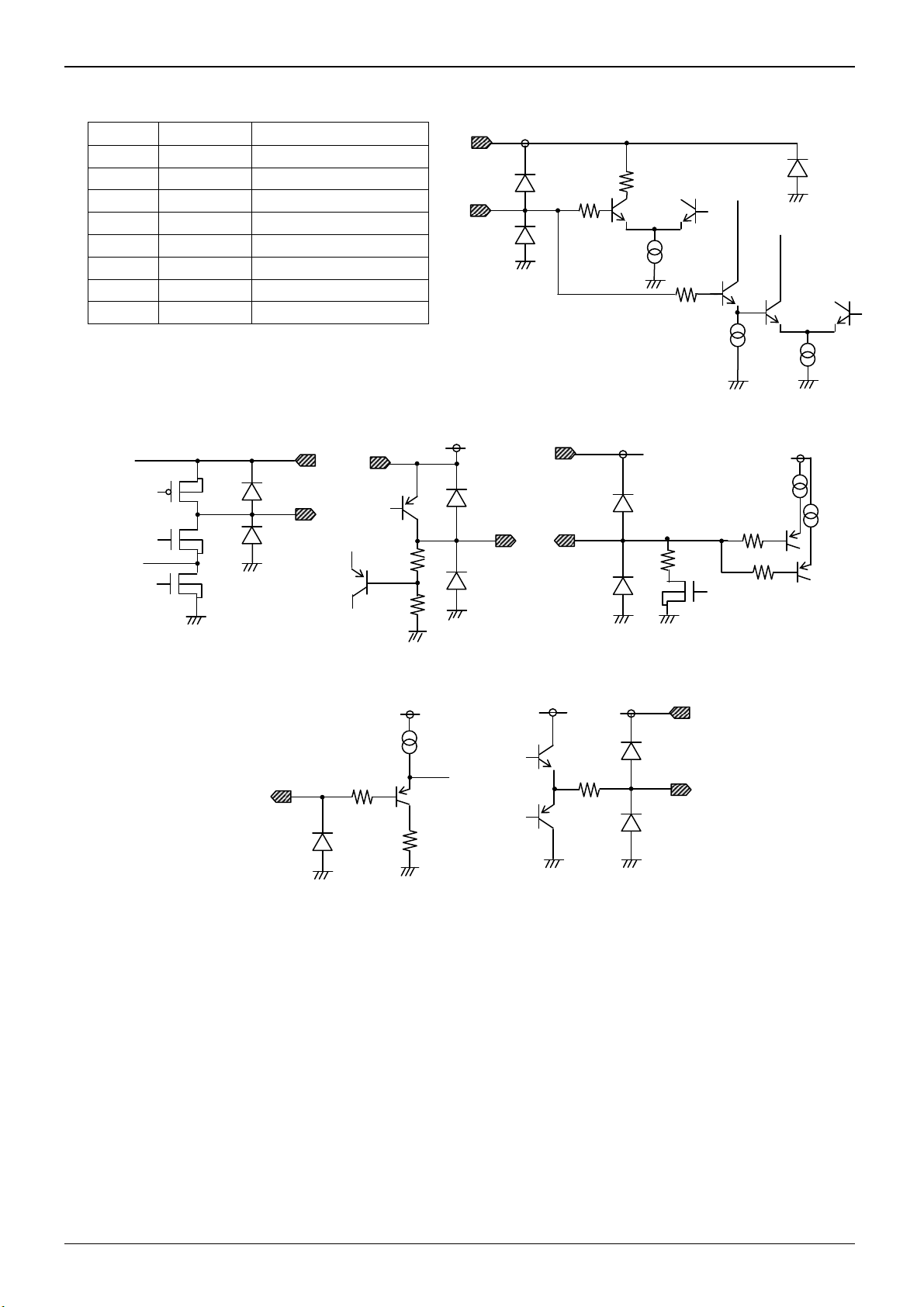
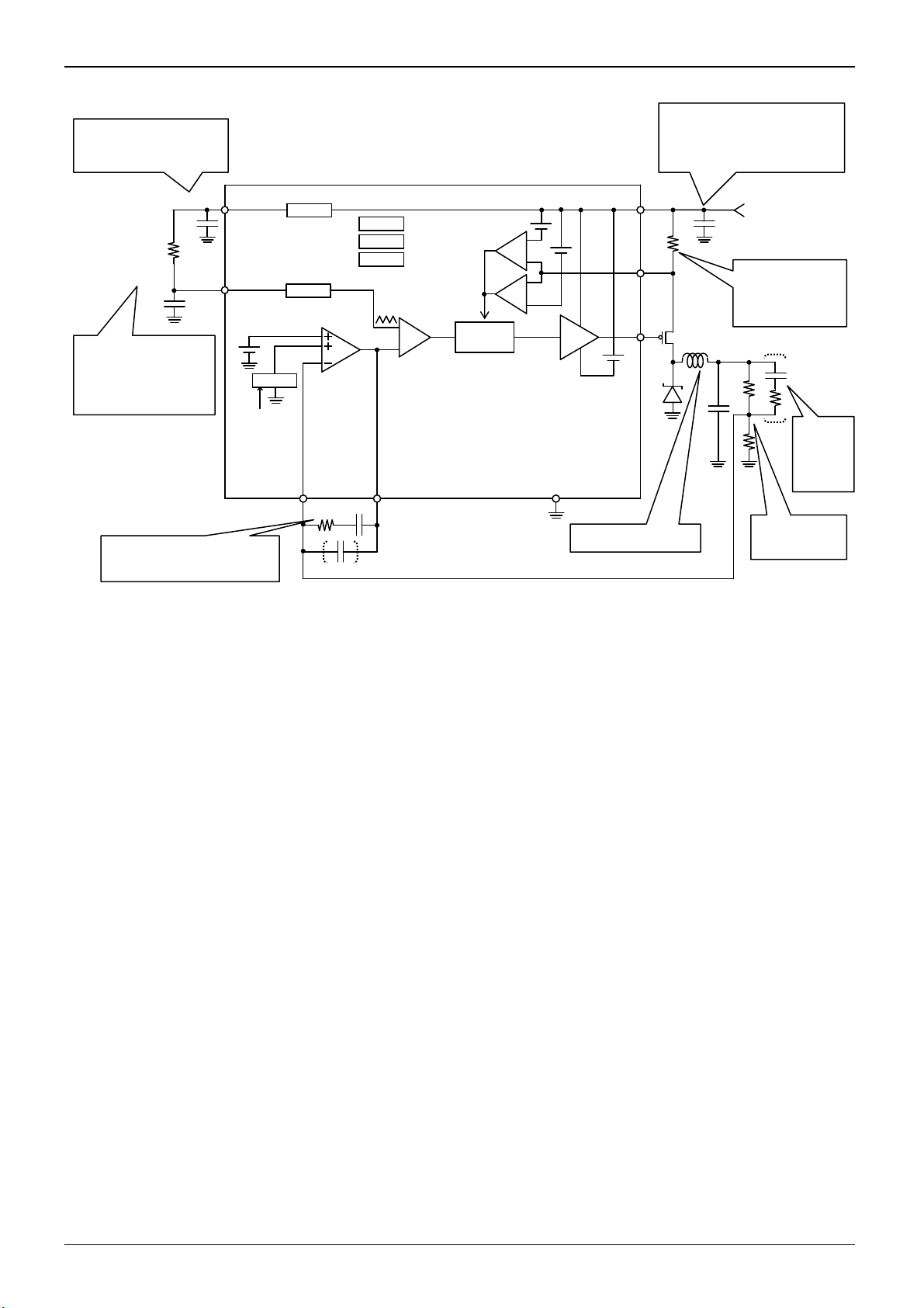
●Pin functions / Block diagram / Application circuit diagram / I/O equivalent circuit diagram
PIN NO. Pin Name Function
1 OSC PWM frequency setting
2 VREF 2.5V regulator output
3 FB Error amplifier output
4 IN- Error amplifier input
5 GATE Gate output
6 CS Current limit input
7 Vcc Power supply
8 GND Ground
IN-
Vcc
50kΩ
50kΩ
VREF
1kΩ
Fig.13 I/O equivalent circuit diagram
Vcc
CS
VREF
VREF
200Ω
Vcc
OSC
Vcc
10Ω
200Ω
5kΩ
FB
Technical Note
VREF
200Ω
200Ω
www.rohm.com
© 2009 ROHM Co., Ltd. All rights reserved.
5/16
2009.11 - Rev.A
Page 6
q
BD63536FJ
Reference voltage output.
Connect a capacitor of 0.1
this pin.
A resistor and capacitor used to
make oscillation frequency
setting. It is recommended to
set the resistor to 20k to 100k
and the capacitor to 100pF to
10nF.
An external resistor and capacitor of
filter used to determine frequency
characteristics
F to
VREF
OSC
Soft Start
GATEOFF
VREG
OSC
UVLO
TSD
OVP
FB IN-
COMP
Controller
C.L.
COMP
GATE
OFF
GND
Fig.14 Typical block diagram / application circuit
VCC
CS
GATE
A smoothing LC filter
Technical Note
A decoupling capacitor.
It is recommended to set this capacitor
F to 100F for electrolytic
to 10
capacitors or 0.01
laminated ceramic capacitors.
F to 0.1F for
V
IN
A resistor used to
detect current. It is
recommended to set
this resistor to 0 to
.
0.3
An external
resistor and
capacitor of
filter used to
determine
fre
uency
A resistor used to
monitor voltage
detection
www.rohm.com
© 2009 ROHM Co., Ltd. All rights reserved.
6/16
2009.11 - Rev.A
Page 7

BD63536FJ
Technical Note
●Description of pins and functions
○VCC: Power supply pin
To apply large drive currents, provide thick and short low impedance wiring, and make current adjustment with careful
attention paid to PWM switching noise so that V
voltage will be stable. It is also possible to arrange laminated ceramic
CC
capacitors of approximately 0.01µ to 0.1µF in parallel with the aim of reducing power supply impedance in a broad frequency
band. Take extra care for V
voltage so that it will not exceed its rating even for a moment. The VCC pin has a built-in clamp
CC
element for electrostatic breakdown protection. If a sudden pulse signal or voltage such as a surge exceeding the absolute
maximum rating is applied, this clamp element may be activated to lead to breakdown. To avoid this, NEVER exceed the
absolute maximum rating. It is also effective to mount a zener diode having a rating approximate to the absolute maximum
rating. In addition, note that since a diode for electrostatic breakdown protection is inserted between the V
pin and the
CC
GND pin, if an inverse voltage is applied to the VCC pin and the GND pin, the IC may lead to breakdown.
○GND: Ground pin
In order to reduce noises due to switching current and stabilize the internal reference voltage of IC, minimize wiring
impedance from this pin and maintain the potential at the minimum level in any operating state. In addition, design patterns
so that the pin has no common impedance to other GND patterns.
○VREF: 2.5V regulator output pin
The VREF pin is a pin used to output internal reference voltage 2.5V (typ.) generated from power supply voltage input to the
pin. In order to stabilize power supply, be sure to connect a 0.1µF capacitor. This pin is also used as a bias power supply.
V
CC
For this application, set a load current to approximately 1mA or less. In addition, note that grounding this pin may pass a
large current through the IC, causing it to break down.
○FB: Error amplifier output pin
The FB pin is an output pin of the feedback error amplifier.
○IN-: Error amplifier input pin
The IN- pin is an input pin of the feedback error amplifier.
○GATE: External FET drive pin
This GATE pin is a pin used to drive the external FET gate. Since output H voltage is “VCC voltage 0.05V (typ)” and output L
voltage is “VCC voltage 5.4V (typ)”, the pin is able to directly drive the external FET gate. Provide thick and short low
impedance wiring from this pin. The GATE pin has a built-in clamp element for electrostatic breakdown protection. If a
sudden pulse signal or voltage such as a surge exceeding the absolute maximum rating is applied, this clamp element may
be activated to lead to breakdown. To avoid this, NEVER exceed the absolute maximum rating. It is also possible to make
switching rate adjustment by mounting a resistor between the GATE pin and the external FET. In addition, note that since the
GATE pin is designed to connect the internal regulator to CMOS output, if voltages between the V
pin and the GATE pin
CC
causes a significant difference by grounding or else, the IC may lead to breakdown.
www.rohm.com
© 2009 ROHM Co., Ltd. All rights reserved.
7/16
2009.11 - Rev.A
Page 8

BD63536FJ
Technical Note
○OSC: PWM oscillation frequency setting capacitance connection pin
The OSC pin is a pin used to produce a triangular waveform for output PWM oscillation frequency and connect an external
resistor and capacitor. By connecting the external resistor and capacitor to this pin, perform charge and discharge. Since H
level for a triangular waveform is 1.4V (typ) and L level is 1.0V (typ), a triangular waveform having an amplitude of
OSC0.4V (typ) is produced. The resistor determines a charge current, and the current is discharged inside the IC through
resistance of 5k (typ). However, at high frequencies in excess of several hundred kHz, OSC amplitude may exceed 0.4V
(typ) due to delay in the internal circuit. To operate the IC at high frequencies, pay careful attention to the frequencies. The
following section shows a characteristics table of capacitance when the external resistor is set to 30k. For example, when
the capacitor is set to 1000pF, frequency “f” will come to 91 [kHz].
Oscillation frequency vs. Capacitance characteristics
1000
OSC周波数Capa特性
R=30KΩ
100
周波数[KHz]
10
Frequency [KHz]
1
10 100 1000 10000 100000
容量値[pF ]
Capacitance [pF]
Fig.15 Typical oscillation frequency characteristics
A calculation formula used to make oscillation frequency setting is shown below.
f
1
7e2)1980R31.0(C
Note that the formula shown above is a reference formula for calculations in the setting range of 470p to 2200pF for the
capacitor and 30k to 100k for the resistor. On application boards, oscillation frequencies may be influenced by wiring capacitance
or the capacity of an oscilloscope used to monitor the frequencies and thereby calculated values may become different from
actual values. Consequently, make it principle to use this formula as a guide for making oscillation frequency setting.
www.rohm.com
© 2009 ROHM Co., Ltd. All rights reserved.
8/16
2009.11 - Rev.A
Page 9

BD63536FJ
Technical Note
○CS: Current detection comparator input pin
The CS pin is an input pin of overcurrent detection circuit comparator. This IC has a built-in overcurent detection circuit
(current limit function) used to turn OFF output current if an abnormal overcurrent such as short-circuited output current flows
through the IC. This circuit monitors the currents of external FET such as current-sense resistor to input them to the CS pin.
When a voltage input to the CS pin reaches “V
voltage 0.15V (typ)”, the current limit function will be activated. And when
CC
it reaches the current limit voltage, the CS pin will turn OFF output current according to the set resistance and current values.
Subsequently, the pin will be automatically reset when the OSC pin reaches its peak voltage. As just described, the CS pin is
of the automatic resetting type. The CS pin is reset at the peak voltage of the OSC pin and, when the voltage reaches the set
current limit voltage, reset at the same peak voltage again. Then, the CS pin repeats such resetting cycle. Since
superimposing noises onto this pin may cause malfunctions, masking time of approximately 300ns has been internally set. In
addition, it is possible to prevent noises form jumping in the CS pin by adding a capacitor to this pin. Since delay time of
approximately 700ns including the said masking time of approximately 300ns is provided after the current limit is input until it
reaches the GATE pin, if the IC is controlled at a duty cycle of 700ns or less, the current limit function will not be activated.
Normally, no current setting seems to be made to the extent that the CS pin reaches the current limit voltage in the period of
approximately 700ns. However, pay utmost attention to the current setting because it also depends on the external FET. If
the overcurrent detection circuit is not used, short-circuit the CS pin to the V
pin. If a current exceeds the absolute
CC
maximum rating of the CS pin, the IC may break down. To avoid this, pay utmost attention to the current.
A current for the current limit function is set to “0.15V Resistance”. For example, when resistance is 75m, the set current
for the current limit function will come to “2A”.
OSC
CS
GATE
Fig.16 Current limit operation
If a voltage to be input to the CS pin falls below “V
output current. When the CS pin exceeds a voltage of “V
voltage 1V (typ)”, the gate-off function will be activated to turn OFF
CC
voltage 1V (typ)”, the output current will be reset by the soft
CC
start function.
○SOFT START
This IC has a built-in soft start function. This function is used to generate a clock in sync with oscillation inside the IC and
operate the internal 6bitDAC with this clock. Soft start time depends on the oscillation frequency. Taking a frequency 8 times
as high as the oscillation frequency as a reference clock, raise the output voltage at a rate of 40mV/count. The output voltage
will exceed approximately 1.25V at 32 counts. For example, when oscillation frequency f
is set to 100 kHz, a period of
OSC
time required to raise the voltage from 0V to 1.25V will come to approximately 2.56ms from “10µs 8 32 counts”.
Soft start signal
Internal clock
UVLO
Enlargement of internal clock generation
OSC
Fig.17 Soft start operation
www.rohm.com
© 2009 ROHM Co., Ltd. All rights reserved.
9/16
2009.11 - Rev.A
Page 10

BD63536FJ
●Protection circuits
○Thermal shutdown (TSD) circuit
This IC has a built-in thermal shutdown (TSD) circuit as overheat protection. When the IC chip temperature exceeds
175C (typ), GATE output will be turned OFF. When the temperature falls below 155C (typ), the IC will return to the
normal operation. In this case, the normal operation starts up in the soft start sequence. However, if external heat is
continually applied to the IC even when the TSD circuit is in operation, the IC may cause thermal runaway, resulting in
breakdown.
○Overcurrent protection circuit (Current limit function)
This IC has a built-in overcurrent protection circuit. This circuit is a circuit absolutely intended to protect the IC from
breakdown due to overcurrent in abnormal states such as output short circuit, not intended to protect or guarantee sets
with the overcurrent protection circuit incorporated. Consequently, do not design the protection of sets making use of the
function of this circuit. For practical use, take physical safety measures such as use of fuses.
○Undervoltage lockout (UVLO) function
This IC has a built-in undervoltage lockout circuit to prevent malfunctions such as IC output at low power supply voltages.
If power supply voltage falls below the operating voltage range, this UVLO function will be activated. However, if a voltage
applied to the V
provided with hysteresis of approximately 0.15V (typ) in order to prevent malfunctions such as noises. If the UVLO
function is cleared, the IC will start up in the soft start sequence.
○Overvoltage protection (OVP) function
This IC has a built-in overvoltage protection function as a protection circuit for a rise in power supply voltage. If power
supply voltage exceeds the absolute maximum rating, this OVP function will be activated. However, if a voltage applied to
pin exceeds 33.5V (typ), the OVP function will turn OFF the Gate output once. The switching voltage is provided
the V
CC
with hysteresis of approximately 1V (typ) in order to prevent malfunctions such as noises. If the OVP function is reset, the
IC will start up in the soft start sequence.
pin reaches 2.35V (typ), the UVLO function will turn OFF the Gate output once. The switching voltage is
CC
Technical Note
www.rohm.com
© 2009 ROHM Co., Ltd. All rights reserved.
10/16
2009.11 - Rev.A
Page 11

BD63536FJ
Technical Note
●Switching regulator control
Fig. 18 shows the basic configuration of a switching regulator application. The error amplifier determines an output duty
cycle so that a voltage used to monitor output voltage will become equal to the internal reference voltage. The output driver
switches frequency at the said duty cycle, smoothes the switching voltage through the LC filter, and outputs Vout. This IC has
an internal reference voltage of 1.25V (typ) and a recommended output voltage range of 3.3V to 5V. Note that if the output
voltage is set to below 3.3V, for example to 1.25V, the output switching duty cycle may become narrow to disable current limit
setting, depending on oscillation frequency to be used.
VREF
OSC
VREG
OSC
UVLO
TSD
OVP
COMP
Controller
C.L.
COMP
GATE
OFF
Vcc
CS
GATE
Soft Start
GATEOFF
OVP
TSD
UVLO
FB IN-
GND
Fig.18 Switching regulator block diagram
Typical filter circuit
When considering a filter circuit used to determine phase characteristics with the application of this IC, the three patterns
shown in Fig. 19 below are available as a popular way to arrange the filter circuits. The selective use of these circuits is
determined by the relationship between the PWM frequency to be used and the second pole of LC filter, the zero point at
ESR of output capacitor, and ripple elimination rate at the PWM switching frequency to be used.
(a) Filter example 1 (b) Filter example 2 (c) Filter example 3
Fig.19 Examples of filter circuits used to determine phase characteristics
The circuit (a) is the simplest pattern and available for use if the output capacitor has high ESR.
The circuit (b) is a pattern designed by adding a capacitor to the pattern of (a) and available for use if the output capacitor has
high ESR and the voltage ripple elimination rate at the PMW frequency needs to be increased from that of the pattern of (a).
The circuit (c) is a pattern designed by adding two zero-points and thereby available for use even if the output capacitor has
small ESR.
Selectively use the circuits according to the requirement specifications and situations for inductors, capacitors, and PWM
frequency using the patterns shown above.
VIN
www.rohm.com
© 2009 ROHM Co., Ltd. All rights reserved.
11/16
2009.11 - Rev.A
Page 12

v
BD63536FJ
Technical Note
Typical application design
The following section shows a typical application design.
VREF
R
OSC
C
1.25
VREG
OSC
UVLO
TSD
OVP
COMP
Controller
C.L.
COMP
GATE
OFF
Vcc
CS
GATE
Soft Start
GATEOFF、OVP
TSD、UVLO
Rfb1
FB IN-
GND
Rfb2
Fig.20 Typical application design
Example of simple design
The following section shows a design example of constants targeting the applications listed below.
Power supply voltage24V, Output voltage3.3V, Coil47µF, Output capacitor2200µF, Resr0.015, PWM frequency80
kHz, and Load resistance10
1. Determination of values of output voltage detecting resistance
The internal reference voltage is 1.25V and the maximum IN-bias current is 2µA. Consequently, to output Vout of 3.3V,
select resistance values enough to keep from the influence of this bias current, that is, Rfb133k and Rfb220k. In
this case, the ratio of Rfb1 to Rfb2 cannot be changed, but the number of digits of resistance values can be changed.
2. Setting of R (resistance) and C (capacitance) used to make PWM frequency setting
When setting C to 1000pF and R to 39k, the PWM frequency will come to approximately 80 kHz.
3. Determination of L (inductance) and C (capacitance) in accordance with characteristic requirements
This design example is based on L47µF, C2200µF, and Resr0.015.
Reference
Determine a value for the coil to the extent that the system does not enter intermittent mode until it reaches the minimum
value of the preset output current. In this case, however, careful attention should be paid not to cause the coil to become
saturated when the maximum current flows.
Reference formula: L=(Vi-Vo)VoT/ΔILVi [H], where IL
Ripple current of coil, T 1/S
witching frequency
Determine a value for the output capacitor from ESR and output ripple voltage. It is recommended to use a capacity
taking into account enough margin to a value meeting the specification.
Reference formula: ΔVout ΔIL×Resr, where Resr Equivalent series resistance of capacitor
VIN
www.rohm.com
© 2009 ROHM Co., Ltd. All rights reserved.
12/16
2009.11 - Rev.A
Page 13

z
BD63536FJ
4. Selection of filter circuit
For the selection of a filter type, PWM frequency, second pole of LC: “fωp”, and zero point at ESR: “fzesr” are important.
This design example is based on the following:
For this design, PWM frequency is 80 kHz. When looking at unity gain frequency in a total loop with consideration given
to ripple elimination at this frequency, the unity gain frequency should be set in the range of 1/5 to 1/10 of the PWM
frequency, i.e., 8 kHz to 16 kHz. This frequency comes to 10 or more times as high as that for fωp, however the return of
zero point at ESR cannot be expected particularly in the range of 8 kHz to 16 kHz because fz is set to 4.823 kHz. As a
result, design the filter circuit based on the Example (c) shown on the previous page.
5. Determination of filter constant
Look at the design example based on (c). Making an approximate calculation by taking “” as the open loop gain of the
amplifier in this circuit will come to the following formula.
fz
pf
LC
1
Re2
Fig.21 Example (c) of filter circuit used to determine phase characteristics
Vout
)ωj(G
Vin
DC gain
Technical Note
1
1(2
Re
sr
)
R
ππ
0
1
usrC
ππ
1
1
015.0
uu
1(2200472
823.4
10
kH
)
Hz
495
015.022002
)1R1Rfb(Cfωj12R0Cωj1
1Rfb1C0Cωj
Gain
Cf1Rωj12R)1C//0C(ωj1
1
1Rfb)1C0C(
Zero point
Cutoff frequency
The transfer functions of this circuit are shown above. Two zero points can be set. Look at the filter constant using this
circuit as shown below. Approximating phase characteristics in the whole loop with the use of this circuit will come to the
following formula.
Phase Second pole of LC filter Zero point of LC filter First pole of error amplifier
Second pole 90 (1/s) of error amplifier First zero-point of error amplifier
Second zero-point
Make calculations by converting these items into a formula and supposing that unity gain frequency is 8 kHz and phase
margin is 51. Since directly calculating constants results in values in too small digits, the values need to be rounded off.
Then, the constants come to Rfb133k, Rfb220k, R110k, R2120k, C0220pF, C151pF, and Cf1nF. In this
case, when looking at the LC filter on the ideal basis of only the second pole zero point, the unity gain frequency will
be calculated to 10 kHz and the phase margin to approximately 54. Actually, the inductance and capacitance of printed
circuit board will be added, and thereby errors will be caused in calculation results depending on the printed circuit board
used. Consequently, it is considered acceptable to make fine adjustment of resistance and the capacitance of capacitor
with FRA according to the calculation results and then determine the constants.
1fz
1fp
1
Cf)1Rfb1R(π2
1
Cf1Rπ2
2fz
2fp
1
0C2Rπ2
1
)1C//0C(2Rπ2
www.rohm.com
© 2009 ROHM Co., Ltd. All rights reserved.
13/16
2009.11 - Rev.A
Page 14

BD63536FJ
●Notes for Use
(1) Absolute maximum ratings
An excess in the absolute ratings such as applied voltage, operating temperature range, etc. can break down devices,
thus making it impossible to identify a destruction state such as short or open circuit mode. If any special mode to exceed
the absolute maximum ratings is expected, consider adding circuit protection devices such as fuses.
Reverse connection of power supply connector
(2)
Making a reverse connection of the power supply connector can cause the IC to break down.
Power supply line
(3)
If current regenerated by back electromotive force flows back, consider adding protection devices such as insertion of a
capacitor between the power supply and ground as a path of regenerative current and thoroughly check capacitance for
any problems with characteristics such as lack of capacitance of electrolytic capacitors caused at low temperatures, and
then determine the power supply line.
GND potential
(4)
The potential of the GND pin should be maintained at the minimum level in any operating state.
Transient changes
(5)
In this IC, the GATE pin L voltage is set to “V
sudden change due to high switching speed, the voltage can cause transient deviation in excess of “V
(max)”. To avoid this and also protect between the gate and the source of external MOS-FET, it is recommended to insert
and clamp a proper zener diode between the GATE pin and the power supply pin.
Thermal design
(6)
Provide thermal design having a sufficient margin in consideration of power dissipation (Pd) in the practical operating
conditions. Use the thermal design providing as wide radiation pattern as possible in thorough consideration of practical
operating conditions.
Inter-pin shorts and mounting errors
(7)
To mount the IC on printed circuit boards, pay utmost care to the direction and the displacement of the IC. The IC may get
damaged if there is any mounting error or if a short circuit is established due to foreign matter entered between pins. In
addition, thoroughly note that this IC may also get damaged if the VREF pin or GATE pin reaches low potential or is grounded.
Operation in strong magnetic field
(8)
This IC is not designed for operation in the presence of strong magnetic field. To use the IC in a strong magnetic field,
ensure that such use causes the IC not to malfunction.
Thermal-protection circuit (TSD circuit)
(9)
This IC has a built-in thermal-protection circuit (TSD circuit). If chip temperature rises beyond T
will output high voltage and turn OFF the external output transistor. The thermal-protection circuit (TSD circuit) is a circuit
absolutely intended to protect the IC from thermal runaway under abnormal conditions beyond T
to protect or guarantee sets. Consequently, do not design the protection of sets making use of the function of this circuit
TSD ON temperature [°C] (typ.) Hysteresis temperature [°C] (typ.)
175 25
Testing on application board
(10)
When testing the IC on an application board with a capacitor connected to the pin, the IC can be subjected to stress. In this
case, be sure to discharge the capacitor after each process. For static electricity protection, ground the IC during the
assembly process, and further pay utmost attention to the transport and storage of the IC. In addition, to connect the IC to
a jig up to the testing process, be sure to turn OFF prior to connection, and disconnect the IC only after turning OFF the
power supply.
voltage 5.4V (typ)” with the internal regulator of the IC. If output makes a
CC
Technical Note
voltage 6.2V
CC
150C, the GATE pin
jmax
150C, not intended
jmax
www.rohm.com
© 2009 ROHM Co., Ltd. All rights reserved.
14/16
2009.11 - Rev.A
Page 15

BD63536FJ
Technical Note
(12) IC pin input
This monolithic IC contains P Isolation and P substrate layers between adjacent elements in order to keep them isolated.
P-N junctions are formed at the intersections of these P layers and the N layers of other elements, thus making up different
types of parasitic elements.
For example, if a resistor and a transistor is connected with pins respectively as shown in Fig. 22,
○When GND(Pin A) for the resistor, or when GND(Pin B) for the transistor (NPN),
P-N junctions operate as a parasitic diode.
○When GND(Pin B) for the transistor (NPN),
the parasitic NPN transistor operates by the N layer of other element adjacent to the parasitic diode aforementioned.
Due to the structure of the IC, parasitic elements are inevitably formed depending on the relationships of potential. The
operation of parasitic elements can result in interferences in circuit operation, leading to malfunctions and eventually
breakdown of the IC. Consequently, pay utmost attention not to use the IC for any applications by which the parasitic
elements are operated, such as applying a voltage lower than that of GND (P substrate) to the input pin.
Pin A
Parasitic element
N
+
P
P
P
GND
Resistor Transistor (NPN)
B
C
E
N
P
P substrate
GND
+
N N
P substrate
Pin A
Parasitic
element
Pin B
N
+
P
Parasitic element
Pin B
B C
+
P
N
GND
Adjacent other
element
E
GND
Fig.22 Pattern diagram of parasitic elements
Wiring patterns
(13)
Give thorough consideration to power supply and ground wirings, for example, reduce the common impedance and
minimize ripple.
If there are large-current ground and small-signal ground, it is recommended to isolate the large-current ground pattern
from the small-signal ground pattern and ground these patterns to a single reference point on the set so that fluctuations in
voltage due to the resistance of pattern wiring and large current will not result in fluctuations in the voltage of the
small-signal ground. In addition, pay careful attention to the ground wiring patterns of external parts so that no fluctuations
in voltage will be caused.
Parasitic
element
www.rohm.com
© 2009 ROHM Co., Ltd. All rights reserved.
15/16
2009.11 - Rev.A
Page 16

BD63536FJ
●Ordering part number
Technical Note
B D 6 3 5 3 6
(MAX 5.25 include BURR)
6.0±0.3
3.9±0.2
1
0.545
1.375±0.1
0.175
4.9±0.2
234
1.27
Part No.
5678
S
0.42±0.1
0.1
S
4°
+
6°
−4°
0.2±0.1
0.45MIN
(Unit : mm)
SOP-J8
Part No.
F J - E 2
Package
FJ: SOP-J8
<Tape and Reel information>
Embossed carrier tapeTape
Quantity
Direction
of feed
2500pcs
E2
The direction is the 1pin of product is at the upper left when you hold
()
reel on the left hand and you pull out the tape on the right hand
Reel
Packaging and forming specification
E2: Embossed tape and reel
1pin
Order quantity needs to be multiple of the minimum quantity.
∗
Direction of feed
www.rohm.com
© 2009 ROHM Co., Ltd. All rights reserved.
16/16
2009.11 - Rev.A
Page 17

Notes
No copying or reproduction of this document, in part or in whole, is permitted without the
consent of ROHM Co.,Ltd.
The content specied herein is subject to change for improvement without notice.
The content specied herein is for the purpose of introducing ROHM's products (hereinafter
"Products"). If you wish to use any such Product, please be sure to refer to the specications,
which can be obtained from ROHM upon request.
Examples of application circuits, circuit constants and any other information contained herein
illustrate the standard usage and operations of the Products. The peripheral conditions must
be taken into account when designing circuits for mass production.
Great care was taken in ensuring the accuracy of the information specied in this document.
However, should you incur any damage arising from any inaccuracy or misprint of such
information, ROHM shall bear no responsibility for such damage.
The technical information specied herein is intended only to show the typical functions of and
examples of application circuits for the Products. ROHM does not grant you, explicitly or
implicitly, any license to use or exercise intellectual property or other rights held by ROHM and
other par ties. ROHM shall bear no responsibility whatsoever for any dispute arising from the
use of such technical information.
Notice
The Products specied in this document are intended to be used with general-use electronic
equipment or devices (such as audio visual equipment, ofce-automation equipment, communication devices, electronic appliances and amusement devices).
The Products specied in this document are not designed to be radiation tolerant.
While ROHM always makes ef forts to enhance the quality and reliability of its Products, a
Product may fail or malfunction for a variety of reasons.
Please be sure to implement in your equipment using the Products safety measures to guard
against the possibility of physical injury, re or any other damage caused in the event of the
failure of any Product, such as derating, redundancy, re control and fail-safe designs. ROHM
shall bear no responsibility whatsoever for your use of any Product outside of the prescribed
scope or not in accordance with the instruction manual.
The Products are not designed or manufactured to be used with any equipment, device or
system which requires an extremely high level of reliability the failure or malfunction of which
may result in a direct threat to human life or create a risk of human injury (such as a medical
instrument, transportation equipment, aerospace machiner y, nuclear-reactor controller,
fuel-controller or other safety device). ROHM shall bear no responsibility in any way for use of
any of the Products for the above special purposes. If a Product is intended to be used for any
such special purpose, please contact a ROHM sales representative before purchasing.
If you intend to export or ship overseas any Product or technology specied herein that may
be controlled under the Foreign Exchange and the Foreign Trade Law, you will be required to
obtain a license or permit under the Law.
www.rohm.com
© 2009 ROHM Co., Ltd. All rights reserved.
Thank you for your accessing to ROHM product informations.
More detail product informations and catalogs are available, please contact us.
ROHM Customer Support System
http://www.rohm.com/contact/
R0039
A
 Loading...