

Page 1

H-bridge Drivers for Brush Motors
H-bridge Drivers
High current series
BD62231HFP
●Description
BD62321HFP is full bridge driver for brush motor applications. This IC can operate at a wide range of power-supply
voltages (from 6V to 32V), supporting output currents of up to 3A. MOS transistors in the output stage allow for PWM signal
control. The replacement is also easy because of the pin compatible with BD623XHFP series.
●Features
1) Built-in one channel driver
2) Low standby current
3) Supports PWM control signal input (20kHz to 100kHz)
4) Cross-conduction prevention circuit
5) Four protection circuits provided: OCP, OVP, TSD, UVLO and SAP
●Applications
VCR; CD/DVD players; audio-visual equipment; optical disc drives; PC peripherals;OA equipments
●Absolute maximum ratings (Ta=25℃, All voltages are with respect to ground)
Parameter Symbol Ratings Unit
Supply voltage VCC 36 V
Output current I
3.0 *1 A
OMAX
No.11007EBT05
All other input pins VIN -0.3 ~ VCC V
Operating temperature T
Storage temperature T
Power dissipation Pd 1.4 *2 W
Junction temperature T
*1 Do not, exceed Pd or ASO.
*2 HRP7 package. Mounted on a 70mm x 70mm x 1.6mm FR4 glass-epoxy board with less than 3% copper foil. Derated at 11.2mW/℃ above 25℃.
●Operating conditions (Ta=25℃)
Parameter Symbol Ratings Unit
Supply voltage VCC 6 ~ 32 V
-40 ~ +85 ℃
OPR
-55 ~ +150 ℃
STG
150 ℃
jmax
www.rohm.com
© 2011 ROHM Co., Ltd. All rights reserved.
1/10
2011.12 - Rev.B
Page 2
BD62321HFP
●Electrical characteristics (Unless otherwise specified, Ta=25℃ and VCC=24V)
Limits
Parameter Symbol
Unit Conditions
Min. Min. Min.
Supply current ICC 0.7 1.4 2.2 mA Forward / Reverse / Brake
Technical Note
Stand-by current I
- 0 10 µA Stand-by
STBY
Input high voltage VIH 2.0 - - V
Input low voltage VIL - - 0.8 V
Input bias current IIH 30 50 100 µA VIN=5.0V
Output ON resistance RON 0.5 1.0 1.5 Ω IO=1.0A, vertically total
Input frequency range F
20 - 100 kHz FIN / RIN
MAX
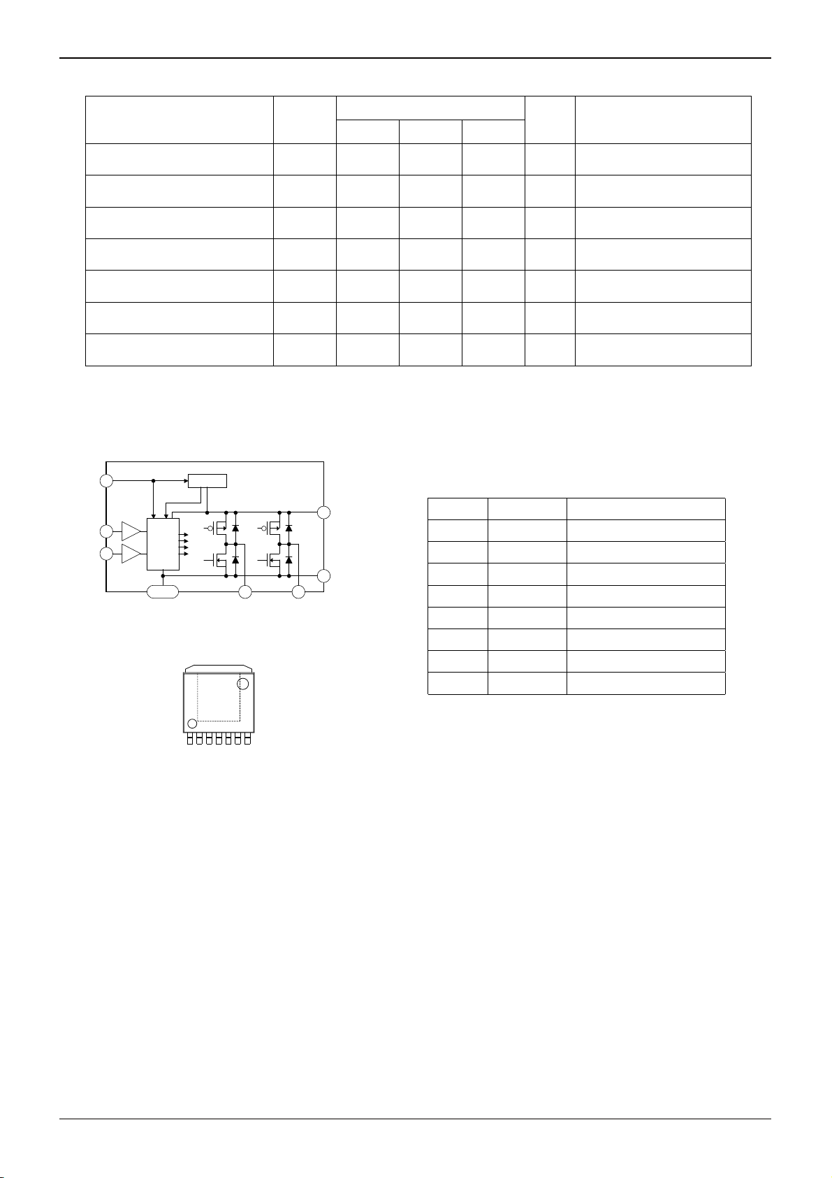
●Block diagram and pin configuration
BD62321HFP
1 VCC
FIN
RIN
3
5
Fig.1 BD62321HFP
CTRL
FIN
GND
PROTECT
OUT1 OUT2
6 2
Table 1 BD62321HFP
VCC
7
Pin Name Function
1 VCC Power supply
2 OUT1 Driver output
GND
4
3 FIN Control input (forward)
4 GND Ground
5 RIN Control input (reverse)
6 OUT2 Driver output
7 VCC Power supply
FIN GND Ground
Note: Use all VCC pin by the same voltage.
VCC
OUT1
FIN
GND
RIN
OUT2
VCC
Fig.2 HRP7 package
www.rohm.com
© 2011 ROHM Co., Ltd. All rights reserved.
2/10
2011.12 - Rev.B
Page 3
BD62321HFP
]
Technical Note
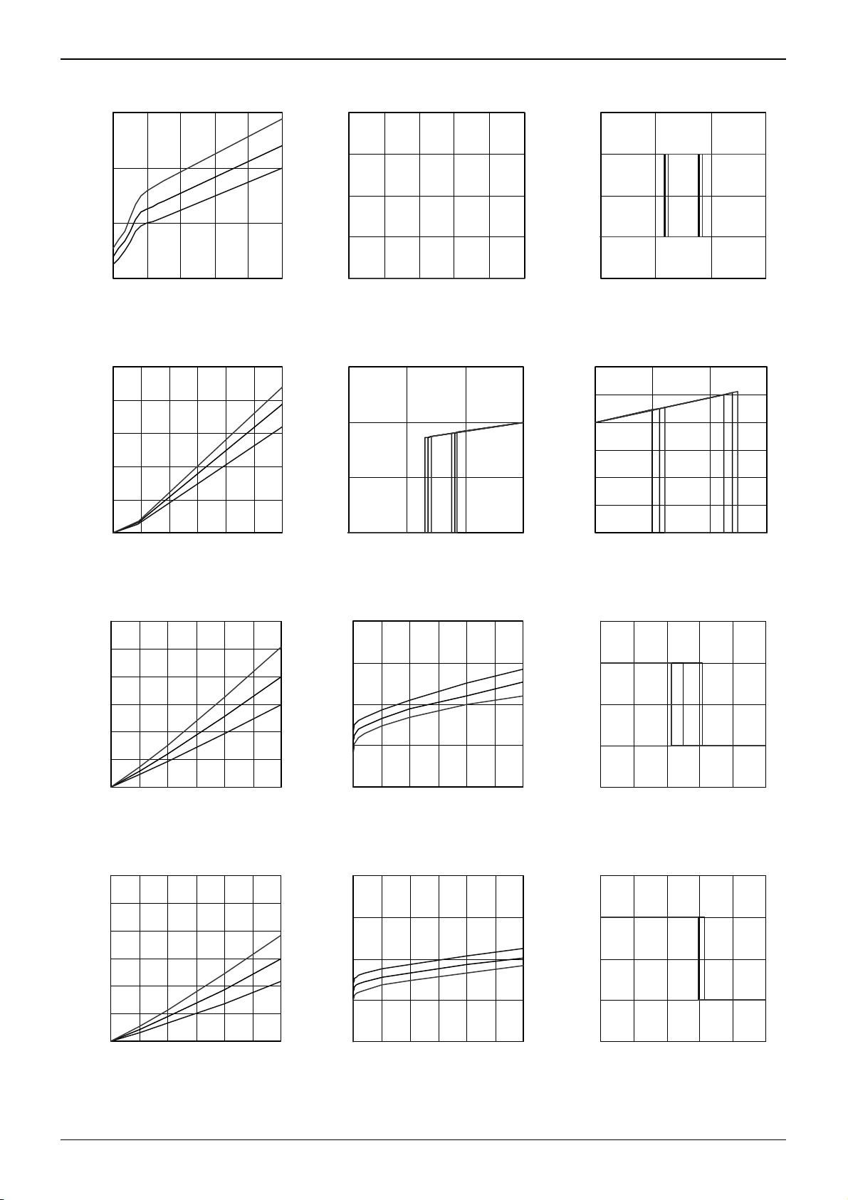
●Electrical characteristic curves (Reference data)
2.0
1.5
1.0
Circuit Current: Icc [mA
0.5
6 1218243036
Supply Voltag e: Vcc [V]
Fig.3 Supply current Fig.4 Stand-by current Fig.5 Input threshold voltage
1.0
0.8
85°C
25°C
-40° C
85°C
25°C
-40° C
0.6
0.4
Input Bias Current: I IH [mA]
0.2
0.0
0 6 12 18 24 30 36
Input Voltag e: VIN [V]
Fig.6 Input bias current Fig.7 Under voltage lock out Fig.8 Over voltage protection
3
2.5
2
1.5
85°C
25°C
-40° C
8
A]
6
4
2
Stand-by Current: ISTBY [
0
6 1218243036
Supply Vol tage: Vc c [V]
9
6
3
Internal signal: Release [V] _
0
4.5 5 5.5 6
Supply Vol tage: VC C [V]
2
1.5
1
-40° C
25°C
85°C
85°C
25°C
-40° C
-40° C
25°C
85°C
1.5
1.0
-40°C
25°C
85°C
0.5
0.0
Internal Logic: H/L [-] _
-0.5
0.8 1.2 1.6 2
Input Vol tage: V IN [ V]
54
45
36
27
85°C
25°C
18
-40° C
9
Internal signal: Release [V] _
0
36 40 44 48
Supply Vol tage: VC C [V]
1.5
1.0
0.5
-40° C
25°C
85°C
85°C
25°C
-40°C
1
0.5
Output Voltage: V CC-VOUT [V]
0.5
Output Voltage:V CC- VOUT [V]
0.0
Internal Logic: H/L [-] _
0
00.511.522.53
Output Current: IOUT [A]
Fig.9 Output high voltage Fig.10 High side body diode Fig.11 Over current protection (H side)
3
2.5
2
1.5
1
Output Voltage: V OUT [V]
0.5
0
00.511.522.53
Output Current: IOUT [A]
85°C
25°C
-40° C
Fig.12 Output low voltage Fig.13 Low side body diode Fig.14 Over current protection (L side)
0
00.511.522.53
Output Current: IOUT [A]
2
1.5
1
0.5
Output Voltage: V OUT [V]
0
00.511.522.53
Output Current: IOUT [A]
-40°C
25°C
85°C
-0.5
4 4.2 4.4 4.6 4.8 5
Load Cur rent [A ]
1.5
1.0
0.5
0.0
Internal Logic: H/L [-] _
-0.5
4 4.2 4.4 4.6 4.8 5
Load Cur rent [A ]
85°C
25°C
-40° C
www.rohm.com
© 2011 ROHM Co., Ltd. All rights reserved.
3/10
2011.12 - Rev.B
Page 4
BD62321HFP
Technical Note
●Functional descriptions
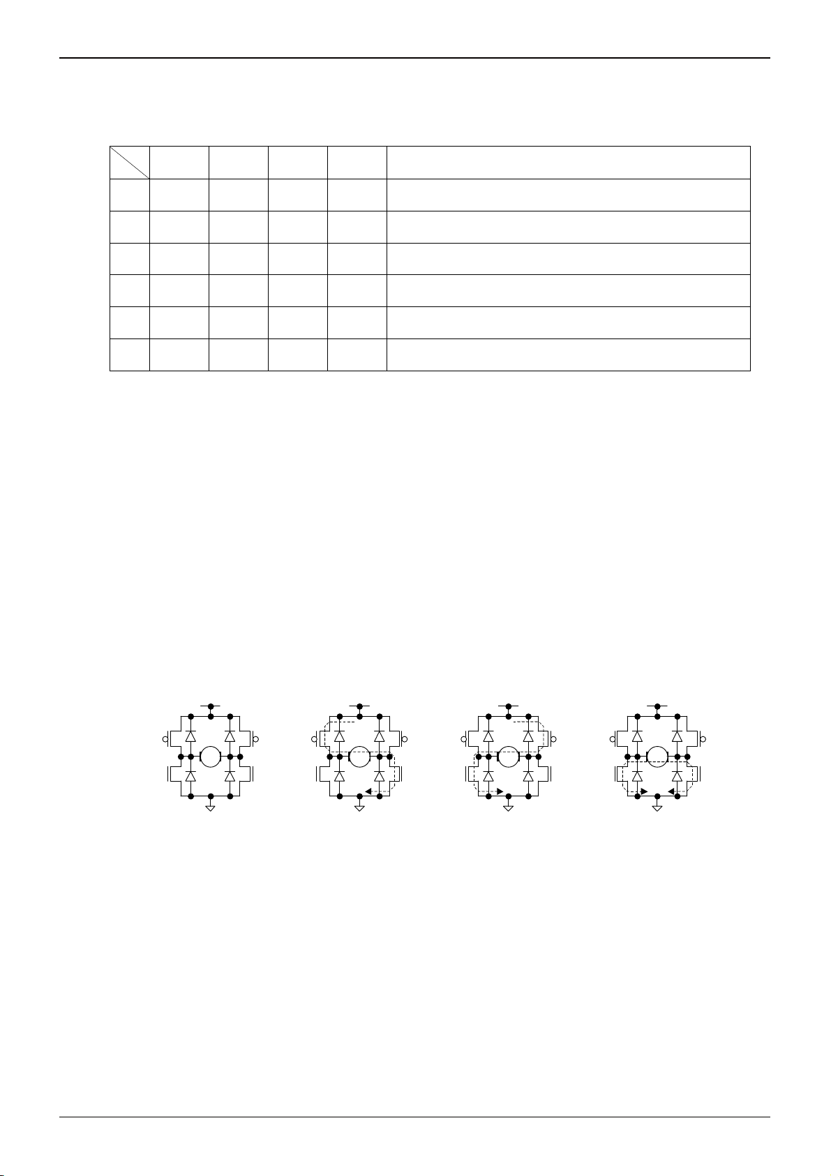
1) Operation modes
Table 2 Logic table
FIN RIN OUT1 OUT2 Operation
a L L Hi-Z* Hi-Z* Stand-by (idling)
b H L H L Forward (OUT1 > OUT2)
c L H L H Reverse (OUT1 < OUT2)
d H H L L Brake (stop)
e PWM L H
f L PWM
* Hi-Z is the off state of all output transistors.
Please note that this is the state of the connected diodes, which differs from that of the mechanical relay.
__________
PWM
__________
PWM
Forward (PWM control)
H Reverse (PWM control)
a) Stand-by mode
In stand-by mode, all internal circuits are turned off, including the output power transistors. Motor output goes to high
impedance. If the motor is running at the switch to stand-by mode, the system enters an idling state because of the
body diodes. However, when the system switches to stand-by from any other mode (except the brake mode), the
control logic remains in the high state for at least 50µs before shutting down all circuits.
b) Forward mode
This operating mode is defined as the forward rotation of the motor when the OUT1 pin is high and OUT2 pin is low.
When the motor is connected between the OUT1 and OUT2 pins, the current flows from OUT1 to OUT2.
c) Reverse mode
This operating mode is defined as the reverse rotation of the motor when the OUT1 pin is low and OUT2 pin is high.
When the motor is connected between the OUT1 and OUT2 pins, the current flows from OUT2 to OUT1.
d) Brake mode
This operating mode is used to quickly stop the motor (short circuit brake). It differs from the stand-by mode because
the internal control circuit is operating in the brake mode. Please switch to the stand-by mode (rather than the brake
mode) to save power and reduce consumption.
OFF
M
OFF
OFF
OFF
ON
OFF
M
OFF
ON
OFF
ON
ON
OFF
M
OFF
ON
M
a) Stand-by mode b) Forward mode c) Reverse mode d) Brake mode
Fig.15 Four basic operations (output stage)
OFF
ON
www.rohm.com
© 2011 ROHM Co., Ltd. All rights reserved.
4/10
2011.12 - Rev.B
Page 5

BD62321HFP
e) f) PWM control mode
The rotational speed of the motor can be controlled by the switching duty when the PWM signal is input to the FIN
pin or the RIN pin. In this mode, the high side output is fixed and the low side output does the switching,
corresponding to the input signal. The switching operates by the output state toggling between "L" and "Hi-Z".
The PWM frequency can be input in the range between 20kHz and 100kHz. Note that control may not be attained by
switching on duty at frequencies lower than 20kHz, since the operation functions via the stand-by mode. Also, circuit
operation may not respond correctly when the input signal is higher than 100kHz. In addition, establish a current path
for the recovery current from the motor, by connecting a bypass capacitor (10µF or more is recommended) between
VCC and ground.
ON
OFF
M
OFF
ON
ON
M
OFF
Control input : H Control input : L
Fig.16 PWM control operation (output stage)
FIN
RIN
OUT1
OUT2
Fig.17 PWM control operation (timing chart)
2) Cross-conduction protection circuit
In the full bridge output stage, when the upper and lower transistors are turned on at the same time, and this condition
exists during the period of transition from high to low, or low to high, a rush current flows from the power supply to
ground, resulting in a loss. This circuit protects against the rush current by providing a dead time (about 800ns,
nominal) at the transition.
3) Output protection circuits
a) Under voltage lock out (UVLO) circuit
To secure the lowest power supply voltage necessary to operate the controller, and to prevent under voltage
malfunctions, a UVLO circuit has been built into this driver. When the power supply voltage falls to 5.3V (nominal) or
below, the controller forces all driver outputs to high impedance. When the voltage rises to 5.5V (nominal) or above,
the UVLO circuit ends the lockout operation and returns the chip to normal operation.
b) Over voltage protection (OVP) circuit
When the power supply voltage exceeds 45V (nominal), the controller forces all driver outputs to high impedance.
The OVP circuit is released and its operation ends when the voltage drops back to 40V (nominal) or below. This
protection circuit does not work in the stand-by mode. Also, note that this circuit is supplementary, and thus if it is
asserted, the absolute maximum rating will have been exceeded. Therefore, do not continue to use the IC after this
circuit is activated, and do not operate the IC in an environment where activation of the circuit is assumed.
c) Thermal shutdown (TSD) circuit
The TSD circuit operates when the junction temperature of the driver exceeds the preset temperature (175℃
nominal). At this time, the controller forces all driver outputs to high impedance. Since thermal hysteresis is provided
in the TSD circuit, the chip returns to normal operation when the junction temperature falls below the preset
temperature (150℃ nominal). Thus, it is a self-returning type circuit.
The TSD circuit is designed only to shut the IC off to prevent thermal runaway. It is not designed to protect the IC or
guarantee its operation in the presence of extreme heat. Do not continue to use the IC after the TSD circuit is
activated, and do not operate
the IC in an environment where activation of the circuit is assumed.
Technical Note
OFF
OFF
www.rohm.com
© 2011 ROHM Co., Ltd. All rights reserved.
5/10
2011.12 - Rev.B
Page 6

BD62321HFP
3
3
d) Over current protection (OCP) circuit
To protect this driver IC from ground faults, power supply line faults and load short circuits, the OCP circuit monitors
the output current for the circuit’s monitoring time (10µs, nominal). When the protection circuit detects an over
current, the controller forces all driver outputs to high impedance during the off time (290µs, nominal). The IC returns
to normal operation after the off time period has elapsed (self-returning type). At the two channels type, this circuit
works independently for each channel.
Threshold
Iout
CTRL Input
Inte rnal status
Monitor / Timer
0
OFF ON
mon.
off timer
Fig.18 Over current protection (timing chart)
e) Safe area protection (SAP) circuit
To protect the output MOS transistors from ASO, ground faults, power supply line faults and load short circuits, the
SAP circuit monitors the conditions for the circuit’s monitoring time (10µs, nominal). When the protection circuit
detects to exceed ASO, the controller forces all driver outputs to high impedance and latch in the state. It is released
that via standby mode during 150µs or more by the control inputs FIN and RIN.
●ASO (Area of Safety Operation)
~Reference data~
10
ON
1msT
T
=10msTON=100ms
ON
10
T
ON
TON=1msTON=10ms
=100ms
T
100µs
ON
[A]
I
1
DS
[A]
DS
I
1
0.1
1 10 100
V
DS
36
[V]
0.1
1 10 100
V
DS
36
[V]
Fig.19 ASO curve (Ta=25℃) Fig.20 ASO curve (Tj=150℃)
When using this IC, set the output transistor so that it does not exceed absolute maximum ratings or ASO.
The output protection circuits are effective only in the area of safety operation.
Technical Note
ON
www.rohm.com
© 2011 ROHM Co., Ltd. All rights reserved.
6/10
2011.12 - Rev.B
Page 7

BD62321HFP
●Thermal design
10.0
8.0
6.0
Pd [W]
4.0
2.0
0.0
0 25 50 75 100 125 150
iv) 4 layers PCB(copper foil: 70mm x 70mm)
iii) 2 layers PCB (copper foil: 70mm x 70mm)
ii) 2 layers PCB (copper foil: 15mm x 15mm)
i) 1 layer PCB (copper foil: 10.5mm x 10.5mm)
iv) 7.3W
iii) 5.5W
ii) 2.3W
i) 1.4W
Mounted on ROHM standard PCB
(70mm x 70mm x 1.6mm FR4 glass-epoxy board)
AMBIENT TEMPERATURE [°C]
Table 3 Thermal resistance
Board
θ
j-a
[℃/W]
Board (4) 17.1
Board (3) 22.7
Board (2) 54.4
Board (1) 89.3
* Transient thermal resistance is measured data only; values are not guaranteed.
Fig.21 Thermal derating curve (HRP7 package)
Thermal design needs to meet the following operating conditions.
In creating the thermal design, sufficient margin must be provided to guarantee the temperature conditions below.
1. The ambient temperature Ta must be 85℃ or below
2. The junction temperature Tj must be 150℃ or below
The junction temperature Tj can be determined using the following equation.
θ
Tj ≈ Ta +
x Pc [℃]
j-a
The power consumption Pc can be determined using the following equation. Refer to page 3 about V
Pc ≈ (I
2
x RON) x D + I
OUT
OUT
x (V
ON(H)
+ V
) x (1 - D) + VCC x ICC [W]
F(H)
ON(H)
Example)
Conditions: Ta=50℃, VCC=24V, Iout=0.5A, D (on duty)=100%.
The power consumption of the IC and the junction temperature are as follows:
Pc ≈ 0.5
2
x 1.0 + 24 x 1.7m = 290.8mW
Tj ≈ 50 + 89.3 x 290.8m = 76 [℃]
Where the Tjmax parameter is 150℃ and the derating is set to 80 percents, the maximum ambient temperature
Tamax is determined as follows.
θ
Ta ≤ Tjmax x 0.8 -
x Pc ≈ 94 [℃]
j-a
In this example, thermal design can be considered satisfactory (meaning that there are no problems in thermal
design), since the system meets the operating temperature conditions.
●Interfaces
VCC
FIN
RIN
100k
100k
OUT1
OUT2
GND
Fig.22 FIN / RIN Fig.23 OUT1 / OUT2
Technical Note
and V
F(H)
.
www.rohm.com
© 2011 ROHM Co., Ltd. All rights reserved.
7/10
2011.12 - Rev.B
Page 8

BD62321HFP
●Notes for use
1) Absolute maximum ratings
Devices may be destroyed when supply voltage or operating temperature exceeds the absolute maximum rating.
Because the cause of this damage cannot be identified as, for example, a short circuit or an open circuit, it is important
to consider circuit protection measures – such as adding fuses – if any value in excess of absolute maximum ratings is
to be implemented.
2) Connecting the power supply connector backward
Connecting the power supply in reverse polarity can damage the IC. Take precautions against reverse polarity when
connecting the power supply lines, such as adding an external direction diode.
3) Power supply lines
Return current generated by the motor’s Back-EMF requires countermeasures, such as providing a return current path
by inserting capacitors across the power supply and GND (10µF, ceramic capacitor is recommended). In this case, it is
important to conclusively confirm that none of the negative effects sometimes seen with electrolytic capacitors –
including a capacitance drop at low temperatures - occurs. Also, the connected power supply must have sufficient
current absorbing capability. Otherwise, the regenerated current will increase voltage on the power supply line, which
may in turn cause problems with the product, including peripheral circuits exceeding the absolute maximum rating. To
help protect against damage or degradation, physical safety measures should be taken, such as providing a voltage
clamping diode across the power supply and GND.
4) Electrical potential at GND
Keep the GND terminal potential to the minimum potential under any operating condition. In addition, check to
determine whether there is any terminal that provides voltage below GND, including the voltage during transient
phenomena. When both a small signal GND and high current GND are present, single-point grounding (at the set’s
reference point) is recommended, in order to separate the small signal and high current GND, and to ensure that
voltage changes due to the wiring resistance and high current do not affect the voltage at the small signal GND. In the
same way, care must be taken to avoid changes in the GND wire pattern in any external connected component.
5) Thermal design
Use a thermal design that allows for a sufficient margin in light of the power dissipation (Pd) under actual operating
conditions.
6) Inter-pin shorts and mounting errors
Use caution when positioning the IC for mounting on printed circuit boards. The IC may be damaged if there is any
connection error, or if pins are shorted together.
7) Operation in strong electromagnetic fields
Using this product in strong electromagnetic fields may cause IC malfunctions. Use extreme caution with
electromagnetic fields.
8) ASO - Area of Safety Operation
When using the IC, set the output transistor so that it does not exceed absolute maximum ratings or ASO.
9) Built-in thermal shutdown (TSD) circuit
The TSD circuit is designed only to shut the IC off to prevent thermal runaway. It is not designed to protect the IC or
guarantee its operation in the presence of extreme heat. Do not continue to use the IC after the TSD circuit is activated,
and do not operate the IC in an environment where activation of the circuit is assumed.
10) Capacitor between output and GND
In the event a large capacitor is connected between the output and GND, if VCC and VIN are short-circuited with 0V or
GND for any reason, the current charged in the capacitor flows into the output and may destroy the IC. Use a capacitor
smaller than 1μF between output and GND.
11) Testing on application boards
When testing the IC on an application board, connecting a capacitor to a low impedance pin subjects the IC to stress.
Therefore, always discharge capacitors after each process or step. Always turn the IC's power supply off before
connecting it to or removing it from the test setup during the inspection process. Ground the IC during assembly steps
as an antistatic measure. Use similar precaution when transporting or storing the IC.
12) Switching noise
When the operation mode is in PWM control, PWM switching noise may effects to the control input pins and cause IC
malfunctions. In this case, insert a pulled down resistor (10kΩ is recommended) between each control input pin and
nd.
grou
Technical Note
www.rohm.com
© 2011 ROHM Co., Ltd. All rights reserved.
8/10
2011.12 - Rev.B
Page 9

BD62321HFP
13) Regarding the input pin of the IC
This monolithic IC contains P+ isolation and P substrate layers between adjacent elements, in order to keep them
isolated. P-N junctions are formed at the intersection of these P layers with the N layers of other elements, creating a
parasitic diode or transistor. For example, the relation between each potential is as follows:
When GND > Pin A and GND > Pin B, the P-N junction operates as a parasitic diode.
When GND > Pin B, the P-N junction operates as a parasitic transistor.
Parasitic diodes inevitably occur in the structure of the IC. The operation of parasitic diodes can result in mutual
interference among circuits, as well as operating malfunctions and physical damage. Therefore, do not use methods by
which parasitic diodes operate, such as applying a voltage lower than the GND (P substrate) voltage to an input pin.
Do not force the voltage of the input pins in excess of 5.5V when the power does not supply to the IC.
Pin A
+
N
P
P
Parasitic element
P
P substrate
GND
+
Technical Note
Resistor Transistor (NPN)
Pin B
Pin A
N N
Parasitic
element
N
Parasitic element
Appendix: Example of monolithic IC structure
B
C
+
P
N
E
P
P substrate
GND
+
P
N
GND
Pin B
B C
E
Parasitic
element
GND
Other adjacent elements
www.rohm.com
© 2011 ROHM Co., Ltd. All rights reserved.
9/10
2011.12 - Rev.B
Page 10

BD62321HFP
●Ordering part number
B D 6 2 3 2 1 H F P - T R
Technical Note
ROHM part
number
HRP7
1.017±0.2
8.0±0.13
0.8875
Type Package
9.395±0.125
(MAX 9.745 include BURR)
8.82±0.1
(5.59)
7654321
1.27
0.08±0.05
0.73±0.1
0.08
S
(7.49)
1.905±0.1
S
0.835±0.2
4.5°
0.27
10.54±0.13
1.523±0.15
+
5.5°
−
4.5°
+0.1
-
0.05
(Unit : mm)
HFP: HRP7
<Tape and Reel information>
Embossed carrier tapeTape
Quantity
Direction
of feed
2000pcs
TR
The direction is the 1pin of product is at the upper right when you hold
( )
reel on the left hand and you pull out the tape on the right hand
Reel
Packaging spec.
TR: Embossed taping
1pin
Direction of feed
Order quantity needs to be multiple of the minimum quantity.
∗
www.rohm.com
© 2011 ROHM Co., Ltd. All rights reserved.
10/10
2011.12 - Rev.B
Page 11

Notes
No copying or reproduction of this document, in part or in whole, is permitted without the
consent of ROHM Co.,Ltd.
The content specied herein is subject to change for improvement without notice.
The content specied herein is for the purpose of introducing ROHM's products (hereinafter
"Products"). If you wish to use any such Product, please be sure to refer to the specications,
which can be obtained from ROHM upon request.
Examples of application circuits, circuit constants and any other information contained herein
illustrate the standard usage and operations of the Products. The peripheral conditions must
be taken into account when designing circuits for mass production.
Great care was taken in ensuring the accuracy of the information specied in this document.
However, should you incur any damage arising from any inaccuracy or misprint of such
information, ROHM shall bear no responsibility for such damage.
The technical information specied herein is intended only to show the typical functions of and
examples of application circuits for the Products. ROHM does not grant you, explicitly or
implicitly, any license to use or exercise intellectual property or other rights held by ROHM and
other parties. ROHM shall bear no responsibility whatsoever for any dispute arising from the
use of such technical information.
The Products specied in this document are intended to be used with general-use electronic
equipment or devices (such as audio visual equipment, ofce-automation equipment, communication devices, electronic appliances and amusement devices).
The Products specied in this document are not designed to be radiation tolerant.
While ROHM always makes efforts to enhance the quality and reliability of its Products, a
Product may fail or malfunction for a variety of reasons.
Please be sure to implement in your equipment using the Products safety measures to guard
against the possibility of physical injury, re or any other damage caused in the event of the
failure of any Product, such as derating, redundancy, re control and fail-safe designs. ROHM
shall bear no responsibility whatsoever for your use of any Product outside of the prescribed
scope or not in accordance with the instruction manual.
The Products are not designed or manufactured to be used with any equipment, device or
system which requires an extremely high level of reliability the failure or malfunction of which
may result in a direct threat to human life or create a risk of human injury (such as a medical
instrument, transpor tation equipment, aerospace machiner y, nuclear-reactor controller, fuelcontroller or other safety device). ROHM shall bear no responsibility in any way for use of any
of the Products for the above special purposes. If a Product is intended to be used for any
such special purpose, please contact a ROHM sales representative before purchasing.
If you intend to export or ship overseas any Product or technology specied herein that may
be controlled under the Foreign Exchange and the Foreign Trade Law, you will be required to
obtain a license or permit under the Law.
Notice
www.rohm.com
© 2011 ROHM Co., Ltd. All rights reserved.
Thank you for your accessing to ROHM product informations.
More detail product informations and catalogs are available, please contact us.
ROHM Customer Support System
http://www.rohm.com/contact/
R1120
A
 Loading...