

Page 1

For brush motors
H-bridge drivers
(18V max.)
BD6220, BD6221, BD6222, BD6225, BD6226, BD6227
zOverview
These H-bridge drivers are full bridge drivers for brush motor applications. Each IC can operate at a wide range of
power-supply voltages (from 3V to 36V), supporting output currents of up to 2A. MOS transistors in the output stage allow
for PWM signal control, while the integrated VREF voltage control function of previous models offers direct replacement of
deprecated motor driver ICs. These highly efficient H-bridge driver ICs facilitate low-power consumption design.
zFeatures
1) Built-in, selectable one channel or two channels configuration
2) Low standby current
3) Supports PWM control signal input (20kHz to 100kHz)
4) VREF voltage setting pin enables PWM duty control
5) Cross-conduction prevention circuit
6) Four protection circuits provided: OCP, OVP, TSD and UVLO
zApplications
VCR; CD/DVD players; audio-visual equipment; optical disc drives; PC peripherals;
car audios; car navigation systems; OA equipments
zLine up matrix
TECHNICAL NOTE
Rating voltage Channels
7V
18V
36V
* Packages; F:SOP8, FV: SSOPB24, HFP:HRP7, FP:HSOP25, FM:HSOPM28
1ch
2ch
1ch
2ch
1ch
2ch
Maximum output current
0.5A 1.0A 2.0A
BD6210
HFP / F
BD6215
FV / FP
BD6220
HFP / F
BD6225
FV / FP
BD6230
HFP / F
BD6235
FV / FP
BD6211
HFP / F
BD6216
FP / FM
BD6221
HFP / F
BD6226
FP / FM
BD6231
HFP / F
BD6236
FP / FM
BD6212
HFP / FP
BD6217
FM
BD6222
HFP / FP
BD6227
FM
BD6232
HFP / FP
BD6237
FM
Aug.2007
Page 2

zAbsolute maximum ratings (Ta=25°C)
Parameter Symbol Ratings Unit
Supply voltage VCC 18 V
Output current IOMAX 0.5 *1 / 1.0 *2 / 2.0 *3 A
All other input pins VIN -0.3 ~ VCC V
Operating temperature TOPR -40 ~ +85 °C
Storage temperature TSTG -55 ~ +150 °C
Power dissipation Pd 0.687 *4 / 0.98 *5 / 1.4 *6 / 1.45 *7 / 2.2 *8 W
Junction temperature Tjmax 150 °C
*** Notes: All voltages are with respect to ground.
*1 BD6220 / BD6225. Do not, exceed Pd or ASO.
*2 BD6221 / BD6226. Do not, exceed Pd or ASO.
*3 BD6222 / BD6227. Do not, exceed Pd or ASO.
*4 SOP8 package. Mounted on a 70mm x 70mm x 1.6mm FR4 glass-epoxy board with less than 3% copper foil. Derated at 5.5mW/°C above 25°C.
*5 SSOPB24 package. Mounted on a 70mm x 70mm x 1.6mm FR4 glass-epoxy board with less than 3% copper foil. Derated at 7.8mW/°C above 25°C.
*6 HRP7 package. Mounted on a 70mm x 70mm x 1.6mm FR4 glass-epoxy board with less than 3% copper foil. Derated at 11.2mW/°C above 25°C.
*7 HSOP25 package. Mounted on a 70mm x 70mm x 1.6mm FR4 glass-epoxy board with less than 3% copper foil. Derated at 11.6mW/°C above 25°C.
*8 HSOPM28 package. Mounted on a 70mm x 70mm x 1.6mm FR4 glass-epoxy board with less than 3% copper foil. Derated at 17.6mW/°C above 25°C.
zOperating conditions (Ta=25°C)
Parameter Symbol Conditions Unit
Supply voltage VCC 6 ~ 15 V
VREF voltage VREF 3 ~ 15 V
z Electrical characteristics (Unless otherwise specified, Ta=25°C and VCC=VREF=12V)
Limits
Parameter Symbol
Unit Conditions
Min. Typ. Max.
Supply current (1ch) ICC 0.8 1.3 2.5 mA Forward / Reverse / Brake
Supply current (2ch) ICC 1.3 2.0 3.5 mA Forward / Reverse / Brake
Stand-by current ISTBY - 0 10 µA Stand-by
Input high voltage VIH 2.0 - - V
Input low voltage VIL - - 0.8 V
Input bias current IIH 30 50 100 µA VIN=5.0V
Output ON resistance *1 RON 1.0 1.5 2.5 Ω IO=0.25A, vertically total
Output ON resistance *2 RON 1.0 1.5 2.5 Ω IO=0.5A, vertically total
Output ON resistance *3 RON 0.5 1.0 1.5 Ω IO=1.0A, vertically total
VREF bias current IVREF -10 0 10 µA VREF=VCC
Carrier frequency FPWM 20 25 35 kHz VREF=9V
Input frequency range FMAX 20 - 100 kHz FIN / RIN
*1 BD6220 / BD6225
*2 BD6221 / BD6226
*3 BD6222 / BD6227
2/16
Page 3

z Electrical characteristic curves (Reference data)
2.0
1.5
1.0
Circuit Current: Icc [mA]
0.5
6 9 12 15 18
85°C
25°C
-40°C
Supply Voltage: Vcc [V]
8
A]
µ
[
6
STBY
4
2
Stand-by Current: I
0
6 9 12 15 18
Supply Voltage: Vcc [V]
-40°C
25°C
85°C
1.5
-40°C
25°C
85°C
1.0
0.5
0.0
Internal Logic: H/L [-]
-0.5
1 1.2 1.4 1.6 1.8 2
Input Voltage: VIN [V]
85°C
25°C
-40°C
Fig.1 Supply current (1ch) Fig.2 Stand-by current Fig.3 Input threshold voltage
400
A]
µ
[
300
IH
200
100
Input Bias Current: I
0
85°C
25°C
-40°C
0 6 12 18
Input Voltage: VIN [V]
10
A]
µ
[
5
VREF
0
-5
Input Bias Current: I
-10
012345
Input Voltage: V
REF
[V]
85°C
25°C
-40°C
1.0
0.8
0.6
0.4
0.2
Switching Duty: D [Ton/T]
0.0
0 0.2 0.4 0.6 0.8 1
Input Voltage: V
REF
-40°C
25°C
85°C
/ VCC [V]
Fig.4 Input bias current Fig.5 VREF input bias current Fig.6 VREF - DUTY
(VCC=12V)
40
[kHz]
PWM
30
20
10
Oscillation Frequency: F
6 9 12 15 18
Supply Voltage: VCC [V]
85°C
25°C
-40°C
9
6
3
85°C
25°C
-40°C
Internal signal: Release [V]
0
44.555.56
Supply Voltage: VCC [V]
35
85°C
25°C
28
-40°C
21
14
7
Internal signal: Release [V]
0
20 24 28 32
Supply Voltage: VCC [V]
Fig.7 VCC - Carrier frequency Fig.8 Under voltage lock out Fig.9 Over voltage protection
1.5
1.0
1.5
1.0
85°C
25°C
-40°C
1.5
1.0
85°C
25°C
-40°C
0.5
0.5
0.5
0.0
Internal Logic: H/L [-]
-0.5
125 150 175 200
Junction T em perature: Tj [°C]
0.0
Internal Logic: H/L [-]
-0.5
22.533.54
Load Current / Iomax: Normalized
0.0
Internal Logic: H/L [-]
-0.5
1 1.25 1.5 1.75 2
Load Current / Iomax: Normalized
Fig.10 Thermal shutdown Fig.11 Over current protection (H side) Fig.12 Over current protection (L side)
3/16
Page 4

z Electrical characteristic curves (Reference data) – Continued
0.4
[V]
OUT
0.3
-V
CC
0.2
85°C
25°C
-40°C
[V]
OUT
-V
CC
0.8
0.6
0.4
85°C
25°C
-40°C
[V]
OUT
-V
CC
1.2
0.9
0.6
85°C
25°C
-40°C
0.1
0.2
0.3
Output Voltage: V
0
0 0.1 0.2 0.3 0.4 0.5
Output Current: I
OUT
[A]
Output Voltage: V
0
0 0.2 0.4 0.6 0.8 1
Output Current: I
OUT
[A]
Output Voltage: V
0
0 0.4 0.8 1.2 1.6 2
Output Current: I
OUT
[A]
Fig.13 Output high voltage (0.5A class) Fig.14 Output high voltage (1A class) Fig.15 Output high voltage (2A class)
[V]
OUT
V
CC-
2
1.5
1
-40°C
25°C
85°C
[V]
OUT
V
CC-
2
1.5
1
-40°C
25°C
85°C
[V]
OUT
V
CC-
2
1.5
1
-40°C
25°C
85°C
0.5
Output Voltage:V
0
0 0.1 0.2 0.3 0.4 0.5
Output Current: I
OUT
[A]
0.5
Output Voltage:V
0
0 0.2 0.4 0.6 0.8 1
Output Current: I
OUT
[A]
0.5
Output Voltage:V
0
0 0.4 0.8 1.2 1.6 2
Output Current: I
OUT
[A]
Fig.16 High side body diode (0.5A class) Fig.17High side body diode (1A class) Fig.18 High side body diode (2A class)
0.4
[V]
0.3
OUT
85°C
25°C
-40°C
[V]
OUT
1.2
0.9
85°C
25°C
-40°C
[V]
OUT
1.2
0.9
85°C
25°C
-40°C
0.2
0.6
0.6
0.1
Output Voltage: V
0
0 0.1 0.2 0.3 0.4 0.5
Output Current: I
OUT
[A]
0.3
Output Voltage: V
0
0 0.2 0.4 0.6 0.8 1
Output Current: I
OUT
[A]
0.3
Output Voltage: V
0
0 0.4 0.8 1.2 1.6 2
Output Current: I
OUT
[A]
Fig.19 Output low voltage (0.5A class) Fig.20 Output low voltage (1A class) Fig.21 Output low voltage (2A class)
[V]
OUT
2
1.5
-40°C
25°C
85°C
[V]
OUT
2
1.5
-40°C
25°C
85°C
[V]
OUT
2
1.5
-40°C
25°C
85°C
1
1
1
0.5
Output Voltage: V
0
0 0.1 0.2 0.3 0.4 0.5
Output Current: I
OUT
[A]
0.5
Output Voltage: V
0
0 0.2 0.4 0.6 0.8 1
Output Current: I
OUT
[A]
0.5
Output Voltage: V
0
0 0.4 0.8 1.2 1.6 2
Output Current: I
OUT
[A]
Fig.22 Low side body diode (0.5A class) Fig.23 Low side body diode (1A class) Fig.24 Low side body diode (2A class)
4/16
Page 5

z Block diagram and pin configuration
BD6220F / BD6221F
6 VREF DUTY
PROTECT
RIN
5
CTRL
4
FIN
OUT1 OUT2
Fig.25 BD6220F / BD6221F
OUT1
VCC
VCC
FIN
GND
OUT2
VREF
RIN
Fig.26 SOP8
BD6220HFP / BD6221HFP / BD6222HFP
VREF DUTY
1
PROTECT
FIN
RIN
3
5
CTRL
FIN
GND
OUT1 OUT2
Fig.27 BD6220/21/22HFP
VREF
OUT1
FIN
GND
RIN
OUT2
VCC
Fig.28 HRP7
VCC
3
VCC
2
Pin Name Function
Table 1 BD6220/21F
1 OUT1 Driver output
2 VCC Power supply
8 GND
7 1
3 VCC Power supply
4 FIN Control input (forward)
5 RIN Control input (reverse)
6 VREF Duty setting pin
7 OUT2 Driver output
8 GND Ground
Table 2 BD6220/21/22HFP
VCC
7
Pin Name Function
1 VREF Duty setting pin
2 OUT1 Driver output
GND
4
6 2
3 FIN Control input (forward)
4 GND Ground
5 RIN Control input (reverse)
6 OUT2 Driver output
7 VCC Power supply
FIN GND Ground
5/16
Page 6

A
A
A
A
A
A
z Block diagram and pin configuration – Continued
BD6222FP
VREF DUTY
17
FIN
20
RIN
19
CTRL
6
GND
PROTECT
FIN
GND
12 1
2 13
OUT1 OUT2
VCC
21
22
VCC
23
7
RNF
8
Fig.29 BD6222FP
OUT1
OUT1
NC
NC
NC
GND
GND
RNF
RNF
NC
NC
NC
OUT2
OUT2
NC
NC
VCC
VCC
VCC
FIN
GND
RIN
NC
VREF
NC
NC
NC
Fig.30 HSOP25
BD6225FV
VREFA DUTY
8
FINA
10
RINA
9
GND
19
VREFB DUTY
20
FINB
RINB
22
21
CTRL
CTRL
PROTECT
PROTECT
VCC
23
VCC
24
OUT1A
1
OUT2A
5
RNFA
3
VCC
11
VCC
12
OUT1B
13
OUT2B
17
GND
7
RNFB
15
Fig. 31 BD6225FV
OUT1
RNF
OUT2
GND
VREF
RIN
FIN
VCC
VCC
NC
NC
NC
VCC
VCC
FINB
RINB
VREFB
GND
NC
OUT2B
NC
RNFB
NC
OUT1B
Fig. 32 SSOPB24
Table 3 BD6222FP
Pin Name Function
1,2 OUT1 Driver output
6 GND Small signal ground
7,8 RNF Power stage ground
12,13 OUT2 Driver output
17 VREF Duty setting pin
19 RIN Control input (reverse)
20 FIN Control input (forward)
21 VCC Power supply
22,23 VCC Power supply
FIN GND Ground
Note: All pins not described above are NC pins.
Table 4 BD6225FV
Pin Name Function
1 OUT1A Driver output
3 RNFA Power stage ground
5 OUT2A Driver output
7 GND Small signal ground
8 VREFA Duty setting pin
9 RINA Control input (reverse)
10 FINA Control input (forward)
11 VCC Power supply
12 VCC Power supply
13 OUT1B Driver output
15 RNFB Power stage ground
17 OUT2B Driver output
19 GND Small signal ground
20 VREFB Duty setting pin
21 RINB Control input (reverse)
22 FINB Control input (forward)
23 VCC Power supply
24 VCC Power supply
Note: All pins not described above are NC pins.
6/16
Page 7

A
A
A
A
A
A
A
A
A
A
A
A
z Block diagram and pin configuration – Continued
BD6225FP, BD6226FP/FM
CTRL
PROTECT
VCC
24
VCC
25
OUT1A
1
OUT2A
6
VREFA DUTY
9
FINA
RINA
11
10
GND
20
VREFB DUTY
21
FINB
23
RINB
22
GND
8
PROTECT
CTRL
FIN
GND
RNFA
3
VCC
12
VCC
13
OUT1B
14
OUT2B
19
RNFB
16
Fig. 33 BD6225FP, BD6226FP
OUT1
RNF
OUT2
GND
GND
VREF
RIN
FIN
VCC
VCC
NC
NC
NC
NC
VCC
VCC
FINB
RINB
VREFB
GND
GND
OUT2B
NC
NC
RNFB
NC
OUT1B
Fig. 34 HSOP25
OUT1
RNF
OUT2
GND
NC
NC
NC
NC
VCC
NC
VCC
FINB
RINB
VREFB
GND
GND
GND
VREF
RIN
FIN
VCC
VCC
NC
NC
OUT2B
NC
NC
RNFB
NC
OUT1B
Fig. 35 HSOPM28
Table 5 BD6225F P / BD6226FP
Pin Name Function
1 OUT1A Driver output
3 RNFA Power stage ground
6 OUT2A Driver output
8 GND Small signal ground
9 VREFA Duty setting pin
10 RINA Control input (reverse)
11 FINA Control input (forward)
12 VCC Power supply
13 VCC Power supply
14 OUT1B Driver output
16 RNFB Power stage ground
19 OUT2B Driver output
20 GND Small signal ground
21 VREFB Duty setting pin
22 RINB Control input (reverse)
23 FINB Control input (forward)
24 VCC Power supply
25 VCC Power supply
FIN GND Ground
Note: All pins not described above are NC pins.
Table 6 BD6226FM
Pin Name Function
1 OUT1A Driver output
3 RNFA Power stage ground
6 OUT2A Driver output
8 GND Small signal ground
9 VREFA Duty setting pin
10 RINA Control input (reverse)
11 FINA Control input (forward)
12 VCC Power supply
14 VCC Power supply
15 OUT1B Driver output
17 RNFB Power stage ground
20 OUT2B Driver output
22 GND Small signal ground
23 VREFB Duty setting pin
24 RINB Control input (reverse)
25 FINB Control input (forward)
26 VCC Power supply
28 VCC Power supply
FIN GND Ground
Note: All pins not described above are NC pins.
7/16
Page 8

A
A
A
A
A
A
F
A
A
A
z Block diagram and pin configuration – Continued
BD6227FM
VREFA DUTY
9
FINA
RINA
11
10
GND
22
VREFB DUTY
23
FINB
RINB
25
24
GND
8
PROTECT
CTRL
PROTECT
CTRL
FIN
GND
VCC
26
27
VCC
28
1
OUT1A
2
6
OUT2A
7
3
RNFA
4
VCC
12
13
VCC
14
15
OUT1B
16
20
OUT2B
21
17
RNFB
18
Fig. 36 BD6227FM
OUT1
OUT1
RNF
RNF
OUT2
OUT2
NC
VCC
VCC
VCC
FINB
RINB
VREFB
GND
GND
GND
VRE
GND
RIN
FIN
VCC
VCC
VCC
OUT2B
OUT2B
NC
RNFB
RNFB
OUT1B
OUT1B
Fig. 37 HSOPM28
Table 7 BD6227FM
Pin Name Function
1,2 OUT1A Driver output
3,4 RNF A Power stage ground
6,7 OUT2A Driver output
8 GND Small signal ground
9 VREFA Duty setting pin
10 RINA Control input (reverse)
11 FINA Control input (forward)
12 VCC Power supply
13,14 VCC Power supply
15,16 OUT1B Driver output
17,18 RNFB Power stage ground
20,21 OUT2B Driver output
22 GND Small signal ground
23 VREFB Duty setting pin
24 RINB Control input (reverse)
25 FINB Control input (forward)
26 VCC Power supply
27,28 VCC Power supply
FIN GND Ground
Note: All pins not described above are NC pins.
8/16
Page 9

zFunctional descriptions
1) Operation modes
FIN RIN VREF OUT1 OUT2 Operation
a L L X Hi-Z* Hi-Z* Stand-by (idling)
b H L VCC H L Forward (OUT1 > OUT2)
c L H VCC L H Reverse (OUT1 < OUT2)
d H H X L L Brake (stop)
e PWM L VCC H PWM
f L PWM VCC PWM
g H L Option H PWM
h L H Option PWM
* Hi-Z is the off state of all output transistors. Please note that this is the state of the connected diodes, which differs from that of the mechanical relay.
X : Don’t care
a) Stand-by mode
Stand-by operates independently of the VREF pin voltage. In stand-by mode, all internal circuits are turned off,
including the output power transistors. Motor output goes to high impedance. If the motor is running at the switch to
stand-by mode, the system enters an idling state because of the body diodes. However, when the system switches
to stand-by from any other mode (except the brake mode), the control logic remains in the high state for at least
50µs before shutting down all circuits.
b) Forward mode
This operating mode is defined as the forward rotation of the motor when the OUT1 pin is high and OUT2 pin is low.
When the motor is connected between the OUT1 and OUT2 pins, the current flo ws from OUT1 to OUT2. For
operation in this mode, connect the VREF pin with VCC pin.
c) Reverse mode
This operating mode is defined as the reverse rotation of the motor when the OUT1 pin is low and OUT2 pin is high.
When the motor is connected between the OUT1 and OUT2 pins, the current flo ws from OUT2 to OUT1. For
operation in this mode, connect the VREF pin with VCC pin.
d) Brake mode
This operating mode is used to quickly stop the motor (short circuit brake). It differs from the stand-by mode
because the internal control circuit is operating in the brake mode. Please switch to the stand-by mode (rather than
the brake mode) to save power and reduce consumption.
OFF
OFF
a) Stand-by mode b) Forward mode c) Reverse mode d) Brake mode
M
OFF
OFF
Table 8 Logic table
Forward (PWM control)
Forward (VREF control)
OFF
OFF
ON
ON
ON
OFF
H Reverse (PWM control)
H Reverse (VREF control)
M
Fig.38 Four basic operations (output stage)
M
ON
OFF
OFF
ON
OFF
M
ON
9/16
Page 10

e) f) PWM control mode
The rotational speed of the motor can be controlled by the switching duty when the PWM signal is input to the FIN
pin or the RIN pin. In this mode, the high side output is fixed and the low side output does the switching,
corresponding to the input signal. The switching operates by the output state toggling between "L" and "Hi-Z".
The PWM frequency can be input in the range between 20kHz and 100kHz. Note that control ma y not be attained
by switching on duty at frequencies lower than 20kHz, since the operation functions via the stand-by mode. Also,
circuit operation may not respond correctly when the input signal is higher than 100kHz. To operate in this mode,
connect the VREF pin with VCC pin. In addition, establish a current path for the recovery current from the motor , by
connecting a bypass capacitor (10µF or more is recommended) between VCC and ground.
ON
OFF
M
OFF
ON
ON
OFF
Control input : H Control input : L
Fig.39 PWM control operation (output stage)
FIN
RIN
OUT1
OUT2
Fig.40 PWM control operation (timing chart)
g) h) VREF control mode
The built-in VREF-switching on duty conversion circuit provides switching duty correspon ding to the voltage of the
VREF pin and the VCC voltage. The function offers the same level of control as the high voltage output setting
function in previous models. The on duty is shown by the following equation.
DUTY ≈ VREF [V] / VCC [V]
For example, if VCC voltage is 12V and VREF pin voltage is 9V, the switching on duty is about 75 percent.
However, please note that the switching on duty might be limited by the range of VREF pin voltage (Refer to the
operating conditions, shown on page 2). The PWM carrier frequency in this mode is 25kHz (nominal), and the
switching operation is the same as it is the PWM control modes. When operating in this mode, do not input the
PWM signal to the FIN and RIN pins. In addition, establish a current path for the recovery current from the motor,
by connecting a bypass capacitor (10µF or more is recommended) between VCC and ground.
VCC
VREF
0
FIN
RIN
OUT1
OUT2
Fig.41 VREF control operation (timing chart)
OFF
M
OFF
10/16
Page 11

2) Cross-conduction protection circuit
In the full bridge output stage, when the upper and lower transistors are turned on at the same time, and this condition
exists during the period of transition from high to low, or low to high, a rush current flows from the power supply to
ground, resulting in a loss. This circuit protects against the rush current by providing a dead time (about 400ns,
nominal) at the transition.
3) Output protection circuits
a) Under voltage lock out (UVLO) circuit
To secure the lowest power supply voltage necessary to operate the controller, and to prevent under voltage
malfunctions, a UVLO circuit has been built into this driver. When the power supply voltage falls to 5.0V (nominal)
or below, the controller forces all driver outputs to high impedance. When the voltage rises to 5.5V (nominal) or
above, the UVLO circuit ends the lockout operation and returns the chip to normal operation.
b) Over voltage protection (OVP) circuit
When the power supply voltage exceeds 30V (nominal), the controller forces all driver outputs to high i mpedance.
The OVP circuit is released and its operation ends when the voltage drops back to 25V (nominal) or below. This
protection circuit does not work in the stand-by mode. Also, note that this circuit is supplementary, and thus if it is
asserted, the absolute maximum ra ting will have been ex ceeded. Therefore, do not continue to use the IC after this
circuit is activated, and do not operate the IC in an environment where activation of the circuit is assumed.
c) Thermal shutdown (TSD) circuit
The TSD circuit operates when the junction temperature of the driver exceeds th e preset temperature (175°C
nominal). At this time, the controller forces all driver outputs to high impedance. Since thermal hysteresis is
provided in the TSD circuit, the chip returns to normal operation when the junction temperature falls below the
preset temperature (150°C nominal). Thus, it is a self-returning type circuit.
The TSD circuit is designed only to shut the IC off to prevent thermal runaway. It is not designed to protect the IC or
guarantee its operation in the presence of extreme heat. Do not continue to use the IC after the TSD circuit is
activated, and do not operate the IC in an environment where activation of the circuit is assumed.
d) Over current protection (OCP) circuit
To protect this driver IC from ground faults, power supply line faults and load short circuits, the OCP circuit
monitors the output current for the circuit’s monitoring time (10µs, nominal). When the protection circuit detects an
over current, the controller forces all driver outputs to high impedance during the off time (290µs, nominal). The IC
returns to normal operation after the off time period has elapsed (self-returning type). At the tw o channels type, this
circuit works independently for each channel.
Threshold
Iout
CTRL Input
Internal status
Monitor / Timer
0
mon.
OFF ON
off timer
ON
Fig.42 Over current protection (timing chart)
1 1 /16
Page 12

z Thermal design
Pd [W]
10.0
8.0
6.0
4.0
2.0
0.0
i) Package onl y (copper foi l: 10.5mm x 10. 5m m )
ii ) 2 l ayers P CB (coppe r f o i l : 15 m m x 15m m )
iii) 2 lay er s PCB (c oppe r foil: :70mm x 70 mm)
iv) 4 layers PCB (copper f oi l : 70m m x 70m m )
iv) 7.3W
iii) 5.5W
ii) 2.3W
i) 1.4W
0 25 50 75 100 125 150
AMBIENT TEM PERATURE [°C]
1.5
Pd [W]
i) Package only
ii) Mounted on ROHM standard PCB
(70mm x 70m m x 1. 6mm FR4 glass-epoxy board)
1.0
ii) 0.687W
0.5
i) 0.562W
Pd [W]
1.5
i) Package only
ii) Mounted on ROHM standard PCB
(70mm x 70mm x 1.6m m FR4 glass-epoxy board)
1.0
0.5
ii) 0.976W
i) 0.787W
0.0
0 25 50 75 100 125 150
AMBIENT TEM PERATURE [°C]
0.0
0 25 50 75 100 125 150
AMBIENT TEM PERATURE [°C]
Fig.43 Thermal derating curve Fig.44 Thermal derating curve Fig.45 Thermal derating curve
(SOP8) (SSOPB24) (HRP7)
3
Pd [W]
i) Package only
ii) Mounted on ROHM standard PCB
(70mm x 70mm x 1. 6m m F R4 glass-epoxy board)
2
ii) 1.45W
1
i) 0.85W
0
0 25 50 75 100 125 150
AMBIENT TEMPERATURE [°C]
3
i) Package only
ii) Mounted on ROHM standard PCB
(70mm x 70mm x 1. 6m m F R4 glass-epoxy board)
2
ii) 2.20W
i) 1.80W
Pd [W]
1
0
0 25 50 75 100 125 150
AMBIENT TEMPERATURE [°C]
Table 9 Thermal resistance
Package
θ
[°C/W]
j-a
SOP8 182
SSOPB24 122
HRP7 89.3
HSOP25 86.2
HSOP28 56.8
Mounted on a 70mmx70mmx1.6mm FR4 glass- epoxy
board with less than 3% copper foil.
Fig.46 Thermal derating curve Fig.47 Thermal derating curve
(HSOP25) (HSOPM28)
Thermal design needs to meet the following operating conditions.
In creating the thermal design, sufficient margin must be provided to guarantee the temperature conditions below.
1. The ambient temperature Ta must be 85°C or below
2. The junction temperature Tj must be 150°C or below
The junction temperature Tj can be determined using the following equation.
θ
Tj ≈ Ta +
x Pc [°C]
j-a
The power consumption Pc can be determined using the following equation. Refer to page 4 about V
ON(H)
and V
F(H)
.
Pc ≈ (I
x RON) x (V
OUT
/ VCC) + I
REF
OUT
x (V
ON(H)
+ V
) x (1 - V
F(H)
/ VCC) + VCC x ICC [W]
REF
2
Example using the BD6221F
Conditions: Ta=50°C, VCC=VREF=12V, Iout=0.1A.
The power consumption of the IC and the junction temperature are as follows:
2
Pc ≈ 0.1
x 1.5 + 12 x 1.3m = 30.6mW
Tj ≈ 50 + 182 x 30.6m = 55.6 [°C]
Where the Tjmax parameter is 150°C and the derating is set to 80 percents, the maximum ambient temperature
Tamax is determined as follows.
θ
Ta ≤ Tjmax x 0.8 -
x Pc ≈ 115 [°C]
j-a
In this example, thermal design can be considered satisfactory (meaning that there are no problems in thermal design),
since the system meets the operating temperature conditions.
12/16
Page 13

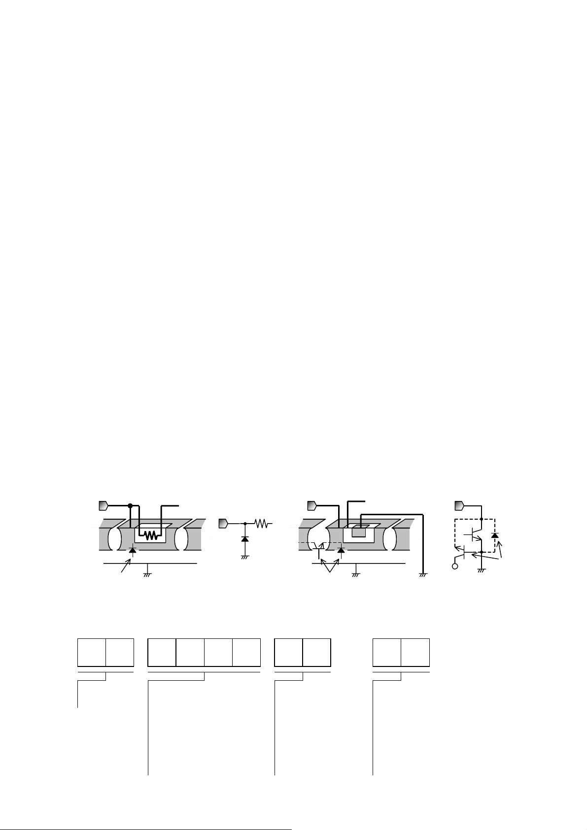
zInterfaces
FIN
RIN
VCC
100k
100k
VREF
VCC
10k
VCC
OUT1
OUT2
GND
Fig.48 FIN / RIN Fig.49 VREF Fig.50 OUT1 / OUT2 Fig.51 OUT1 / OUT2
(SOP8/HRP7) (SSOPB24/HSOP25/HSOPM28)
zNOTES FOR USE
1) Absolute maximum ratings
Devices may be destroyed when supply voltage or operating tem perature exceeds the absolute maximum rating.
Because the cause of this damage cannot be identified as, for example, a short circuit or an open circuit, it is important
to consider circuit protection measures – such as adding fuses – if any value in excess of absolute maximum ratings is
to be implemented.
2) Connecting the power supply connector backward
Connecting the power supply in reverse polarity can damage the IC. Take precautions against reverse polarity when
connecting the power supply lines, such as adding an external direction diode.
3) Power supply lines
Return current generated by the motor’s Back-EMF requires countermeasures, such as providing a return current path
by inserting capacitors across the power supply and GND. In this case, it is important to conclusively confirm that none
of the negative effects sometimes seen with electrolytic capacitors – including a capacitance drop at low temperatures
- occurs. Also, the connected power supply must have sufficient current absorbing capability. Otherwise, the
regenerated current will increase voltage on the power supply line, which may in turn cause problems with the product,
including peripheral circuits exceeding the absolute maximum rating. To help protect against damage or degradation,
physical safety measures should be taken, such as providing a voltage clamping diode across the power supply and
GND.
4) Electrical potential at GND
Keep the GND terminal potential to the minimum potential under any operating condition. In addition, check to
determine whether there is any terminal that provides voltage below GND, including the voltage during transient
phenomena. When both a small signal GND and high c urrent GND are present, single-point grounding (at the set’s
reference point) is recommended, in order to separate the small signal and high curr ent GND, and to ensure that
voltage changes due to the wiring resistance and high current do not affect the voltage at the small signal GND. In the
same way, care must be taken to avoid changes in the GND wire pattern in any external connected component.
5) Thermal design
Use a thermal design that allows for a sufficient margin in light of the power dissipation (Pd) under actual operating
conditions.
6) Inter-pin shorts and mounting errors
Use caution when positioning the IC for mounting on printed circuit boards. The IC may be damaged if there is any
connection error, or if pins are shorted together.
7) Operation in strong electromagnetic fields
Using this product in strong electromagnetic fields may cause IC malfunctions. Use extreme caution with
electromagnetic fields.
VCC
OUT1
OUT2
RNF
GND
13/16
Page 14
8) ASO - Area of Safety Operation
P
iti
P
iti
When using the IC, set the output transistor so that it does not exceed absolute maximum ratings or ASO.
9) Built-in thermal shutdown (TSD) circuit
The TSD circuit is designed only to shut the IC off to prevent thermal runaway. It is not designed to protect the IC or
guarantee its operation in the presence of extreme heat. Do not continue to use the IC after the TSD circuit is activated,
and do not operate the IC in an environment where activation of the circuit is assumed.
10) Capacitor between output and GND
In the event a large capacitor is connected between the output and GND, if VCC and VIN are short-circuited with 0V or
GND for any reason, the current charged in the capacitor flows into the output and may destroy the IC. Use a capacitor
smaller than 1µF between output and GND.
11) Testing on application boards
When testing the IC on an application board, connecting a capacitor to a low impedance pin subjects the IC to stress.
Therefore, always discharge capacitors after each process or step. Always turn the IC's power supply off before
connecting it to or removing it from the test setup during the inspection process. Ground the IC during assembly steps
as an antistatic measure. Use similar precaution when transporting or storing the IC.
12) Switching noise
When the operation mode is in PWM control or VREF control, PWM switching noise may effects to the control input
pins and cause IC malfunctions. In this case, insert a pulled down resistor (10kΩ is r ecommended) between each
control input pin and ground.
13) Regarding the input pin of the IC
This monolithic IC contains P+ isolation and P substrate layers between adjacent elements, in order to keep them
isolated.
P-N junctions are formed at the intersection of these P layers with the N layers of other elements, creating a parasitic
diode or transistor. For example, the relation between each potential is as follows:
When GND > Pin A and GND > Pin B, the P-N junction operates as a parasitic diode.
When GND > Pin B, the P-N junction operates as a parasitic transistor.
Parasitic diodes inevitably occur in the structure of the IC. The operation of parasitic diodes can result in mutual
interference among circuits, as well as operating malfunctions and physical damage. Therefore, do not use meth ods
by which parasitic diodes operate, such as applying a voltage lower than the GND (P substrate) voltage to an input pin.
Pin A
Parasitic element
N
+
P
P
P
P substrate
GND
+
zOrdering part number
Resistor Transistor (NPN)
Pin B
Pin A
N N
Appendix: Example of monolithic IC structure
aras
element
N
c
Parasitic element
+
P
B
C
E
N
GND
+
P
P
P substrate
N
GND
Pin B
B C
E
aras
element
GND
Other adjacent elements
c
B D 6 2 X X -
ROHM part
number
Type
1X: 7V max.
2X: 18V max.
3X: 36V max.
X0: 1ch/0.5A X5: 2ch/0.5A
X1: 1ch/1A X6: 2ch/1A
Package
F: SOP8
FV: SSOPB24
FP: HSOP25
FM: HSOPM28
HFP: HRP7
Packaging spec.
E2: Embossed taping
(SOP8/SSOPB24
TR: Embossed taping
(HRP7)
X2: 1ch/2A X7: 2ch/2A
14/16
/HSOP25/HSOPM28)
Page 15

y
Di
1234
Di
Di
(
y
p
p
y
Di
<Dimension>
<Dimension>
SSOP-B24
<Dimension>
<Dimension>
4.4±0.2
4.4±0.2
6.2±0.3
6.2±0.3
1.27
1.27
0.11
0.11
1.5±0.1
1.5±0.1
<Dimension>
24
5.6 ± 0.2
7.6 ± 0.3
1
0.1
0.65
1.15 ± 0.1
HSOP25
25 14
7.8 ± 0.3
5.4 ± 0.2
1
0.11
1.9 ± 0.1
HSOP-M28
28 15
9.9 ± 0.3
7.5 ± 0.2
114
0.8
0.11
2.2 ± 0.1
5.0±0.2
5.0±0.2
85
85
0.4±0.1
0.4±0.1
7.8 ± 0.2
13.6 ± 0.2
2.75 ± 0.1
1.95 ± 0.1
0.8
0.36 ± 0.1
18.5 ± 0.2
5.15 ± 0.1
0.35 ± 0.1
0.08
16.0 ± 0.2
41
41
13
12
0.22 ± 0.1
M
0.15±0.1
0.15±0.1
0.1
0.1
0.1
13
0.3Min.
0.3Min.
0.3Min.
0.15 ± 0.1
0.1
0.1 S
0.3Min.
0.25 ± 0.1
0.5 ± 0.2
0.25 ± 0.1
(Unit:mm)
(Unit:mm)
Unit:mm)
(Unit:mm)
(Unit:mm)
<Tape and reel information>
<Tape and reel information>
Tape
Tape
Quantit
Quantit
Direction
Direction
of feed
of feed
Embossed carrier tape
Embossed carrier tape
2500pcs
2500pcs
E2
E2
(Holding the reel with the left hand and pulling the tape out with the right,
(Holding the reel with the left hand and pulling the tape out with the right,
pin 1 will be on the upper left-hand side.)
pin 1 will be on the upper left-hand side.)
1234
1234
1234
Reel
Reel
1234
1234
1234
※When you order , please order in times the amount of package quantity.
※Orders should be placed in multiples of package quantity.
<Tape and Reel information>
Tape
Quantit
Direction
of feed
Embossed carrier ta
2000
cs
E2
(Holding the reel with the left hand and pulling the tape out with the right,
pin 1 will be on the upper left-hand side.)
1234
1234
1234
Reel
※Orders should be placed in multiples of package quantity.
<Tape and reel information>
Tape
Quantity
Direction
of feed
Embossed carrier tape
2000pcs
E2
(Holding the reel with the left hand and pulling the tape out with the right,
pin 1 will be on the upper left-hand side.)
1234
Reel
※Orders should be placed in multiples of package quantity.
<Tape and reel information>
Tape
Quantity
Direction
of feed
Embossed carrier tape
1500pcs
E2
(Holding the reel with the left hand and pulling the tape out with the right,
pin 1 will be on the upper left-hand side.)
1234
Reel
※Orders should be placed in multiples of package quantity.
1Pin
1Pin
1pin
1234
1234
1234
1Pin
1Pin
e
1234
1234
1234
1234
1234
1234
1234
1234
1234
rection of feed
rection of feed
1234
1234
Direction of feed
1234
1234
rection of feed
1234
1234
rection of feed
1234
1234
1234
1234
1234
15/16
Page 16

x x
x x
p
HRP7
<Dimension>
0.8875
9.395 ± 0.125
(MAX 9.745 include BURR)
0.28.0
±
1.017
0.13
±
0.05
±
0.08
8.82 – 0.1
(5.59)
<Tape and reel information>
1.905 ± 0.1
Tape
Quantity
Direction
(7.49)
765432S1
0.73 ± 0.11.27
0.08
0.13
±
0.15
0.2
±
±
10.54
1.523
0.835
+
5.5
-
4.5
4.5
+
0.1
0.27
-
0.05
S
of feed
(Unit:mm)
Embossed carrier tape
cs
2000
TR
(Holding the reel with the left hand and pulling the tape out with the right,
pin 1 will be on the upper right-hand side.)
x x x x x x x x x x x x x x x x
Reel
※Orders should be placed in multiples of package quantity.
1pin
Direction of feed
x x
x x
Catalog NO.05N000A '05.4 ROHM C 3000 TSU
Page 17

Appendix
Notes
No technical content pages of this document may be reproduced in any form or transmitted by any
means without prior permission of ROHM CO.,LTD.
The contents described herein are subject to change without notice. The specifications for the
product described in this document are for reference only. Upon actual use, therefore, please request
that specifications to be separately delivered.
Application circuit diagrams and circuit constants contained herein are shown as examples of standard
use and operation. Please pay careful attention to the peripheral conditions when designing circuits
and deciding upon circuit constants in the set.
Any data, including, but not limited to application circuit diagrams information, described herein
are intended only as illustrations of such devices and not as the specifications for such devices. ROHM
CO.,LTD. disclaims any warranty that any use of such devices shall be free from infringement of any
third party's intellectual property rights or other proprietary rights, and further, assumes no liability of
whatsoever nature in the event of any such infringement, or arising from or connected with or related
to the use of such devices.
Upon the sale of any such devices, other than for buyer's right to use such devices itself, resell or
otherwise dispose of the same, no express or implied right or license to practice or commercially
exploit any intellectual property rights or other proprietary rights owned or controlled by
ROHM CO., LTD. is granted to any such buyer.
Products listed in this document are no antiradiation design.
The products listed in this document are designed to be used with ordinary electronic equipment or devices
(such as audio visual equipment, office-automation equipment, communications devices, electrical
appliances and electronic toys).
Should you intend to use these products with equipment or devices which require an extremely high level
of reliability and the malfunction of which would directly endanger human life (such as medical
instruments, transportation equipment, aerospace machinery, nuclear-reactor controllers, fuel controllers
and other safety devices), please be sure to consult with our sales representative in advance.
It is our top priority to supply products with the utmost quality and reliability. However, there is always a chance
of failure due to unexpected factors. Therefore, please take into account the derating characteristics and allow
for sufficient safety features, such as extra margin, anti-flammability, and fail-safe measures when designing in
order to prevent possible accidents that may result in bodily harm or fire caused by component failure. ROHM
cannot be held responsible for any damages arising from the use of the products under conditions out of the
range of the specifications or due to non-compliance with the NOTES specified in this catalog.
Thank you for your accessing to ROHM product informations.
More detail product informations and catalogs are available, please contact your nearest sales office.
ROHM Customer Support System
www.rohm.com
THE AMERICAS / EUPOPE / ASIA / JAPAN
Contact us : webmaster@ rohm.co. jp
Copyright © 2007 ROHM CO.,LTD.
21, Saiin Mizosaki-cho, Ukyo-ku, Kyoto 615-8585, Japan
TEL : +81-75-311-2121
FAX : +81-75-315-0172
Appendix1-Rev2.0
 Loading...