LED Drivers for LCD Backlights
White Backlight LED Driver
for Medium to Large LCD Panels
(Switching Regulator Type)
BD6150MUV
●Description
BD6150MUV is white LED driver IC with PWM step-up DC/DC converter that can boost max 40V and current driver that can
drive max 30mA. The wide and precision brightness can be controlled by external PWM pulse. BD6150MUV has very
accurate current drivers, and it has few current errors between each strings. So, it will be helpful to reduce brightness spots
on the LCD. Small package type is suited for saving space.
●Features
1) High efficiency PWM step-up DC/DC converter (fsw=1.25MHz / 0.75MHz)
2) High accuracy & good matching current drivers (MAX30mA/ch)
3) Integrated 50V power Nch MOSFET
4) Soft start
5) Drive up to 10 in series 6strings in parallel
6) Wide input voltage range (4.2V ~ 26V)
7) Rich safety functions
・Over-voltage protection ・Over current limit
・LED terminal open/short protect ・External SBD open detect / Output short protection
・UVLO ・Thermal shutdown
8) Small & thin package (VQFN024V4040) 4.0 × 4.0 × 1.0mm
●Applications
All middle size LCD equipments backlight of Notebook PC, portable DVD player, car navigation systems, etc.
●Absolute maximum ratings (Ta=25℃)
Parameter Symbol Ratings Unit Condition
No.11040EBT06
Maximum applied voltage 1 VMAX1 7 V
Maximum applied voltage 2 VMAX2 25 V
Maximum applied voltage 3 VMAX3 30.5 V VBAT, FAILFLAG, PWMPOW
Maximum applied voltage 4 VMAX4 41 V SW
Power dissipation 1 Pd1 500 *1 mW
Power dissipation 2 Pd2 780 *2 mW
Power dissipation 3 Pd3 1510 *3 mW
Operating temperature range Topr -40 ~ +85 ℃
Storage temperature range Tstg -55 ~ +150 ℃
*1 Reduced 4.0mW/℃ With Ta>25℃ when not mounted on a heat radiation Board.
*2 1 layer (ROHM Standard board) has been mounted. Copper foil area 0mm
*3 4 layer (JEDEC Compliant board) has been mounted. Copper foil area 1layer 6.28mm
When it’s used by more than Ta=25℃, it’s reduced by 12.1mW/℃.
2
, When it’s used by more than Ta=25℃, it’s reduced by 6.2mW/℃.
2
, Copper foil area 2~4layers 5655.04mm2,
VREG, ISET, PWMDRV, FSEL,
OCPSET, VDET, TEST
LED1, LED2, LED3,
LED4, LED5, LED6
www.rohm.com
© 2011 ROHM Co., Ltd. All rights reserved.
1/28
2011.06 - Rev.B
BD6150MUV
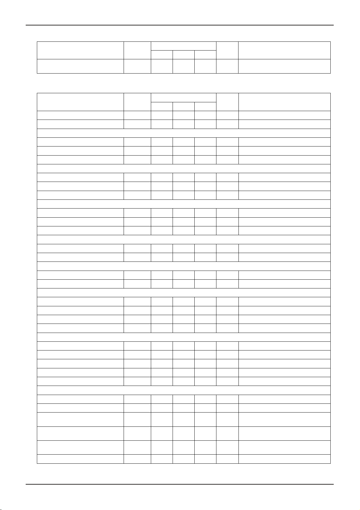
●Recommended operating range (Ta=-40℃ ~ +85℃)
Parameter Symbol
Power supply voltage VBAT 4.2 12.0 26.0 V
●Electrical characteristic (Unless otherwise specified, VBAT=12V, Ta = +25℃)
Parameter Symbol
Quiescent current Iq - 1.6 4.4 µA PWMPOW=0V
Current consumption Idd - 3.2 4.8 mA VDET=0V,ISET=22k
[PWMPOW Terminal]
Low input voltage range1 POWL 0 - 0.9 V
High input voltage range1 POWH 2.1 - VBAT V
Pull down resistor1 POWR 100 300 500 k PWMPOW=3V
[PWMDRV Terminal]
Low input voltage range2 PDRVL 0 - 0.9 V
High input voltage range2 PDRVH 2.1 - 5.5 V
Pull down resistor2 DRVR 100 300 500 k
[FSEL Terminal]
Low input voltage range3 FSL 0 - 0.9 V
High input voltage range3 FSH 2.1 - 6.0 V
Pull down resistor3 FSR 100 300 500 k FSEL=1V
[FAILFLAG]
Input resistor FFIR 1.0 2.0 3.0 k FAILFLAG=2.5V
Off current FFIST - 0.1 2.0 µA PWMPOW=0V
[Regulator]
VREG voltage VREG 4.2 5.0 6.0 V No load
Under voltage lock out UVLO 3.3 3.7 4.1 V VBAT falling edge
[Switching Regulator]
LED control voltage VLED 0.56 0.70 0.84 V
Switching frequency fsw 1.00 1.25 1.50 MHz FSEL=L (GND short)
Duty cycle limit Duty 91 95.0 99.0 % LED1-6=0.3V
SW Nch FET RON RON - 0.48 0.58 ISW=80mA
[Protection]
Over current limit Ocp 1.4 2.0 2.6 A
OCPSET open protect OOP - 0.0 0.1 A OCPSET=2M
Over voltage limit Input Ovl 0.96 1.00 1.04 V Detect voltage of VDET pin
SBD open protect Sop 0.02 0.05 0.08 V Detect voltage of VDET pin
VDET leak current OVIL - 0.1 1.0 µA
[Current driver]
LED maximum current ILMAX - - 30 mA
LED current accuracy ILACCU - - ±3.0 % ILED=16~20mA
LED current matching ILMAT - - ±1.5 %
LED current limiter ILOCP - 0 0.1 mA
Min. Typ. Max.
Min. Typ. Max.
Limits
Limits
Unit Condition
Unit Condition
*1
OCPSET=68k
Each LED current/Average (LED1-6)
ILED=16~20mA
Current limit value at ISET
resistor 1k setting
Technical Note
LED terminal Over voltage protect LEDOVP 10.0 11.5 13.0 V PWMDRV=2.5V
ISET voltage Iset 0.5 0.6 0.7 V
*1 This parameter is tested with DC measurement.
www.rohm.com
© 2011 ROHM Co., Ltd. All rights reserved.
2/28
2011.06 - Rev.B
BD6150MUV
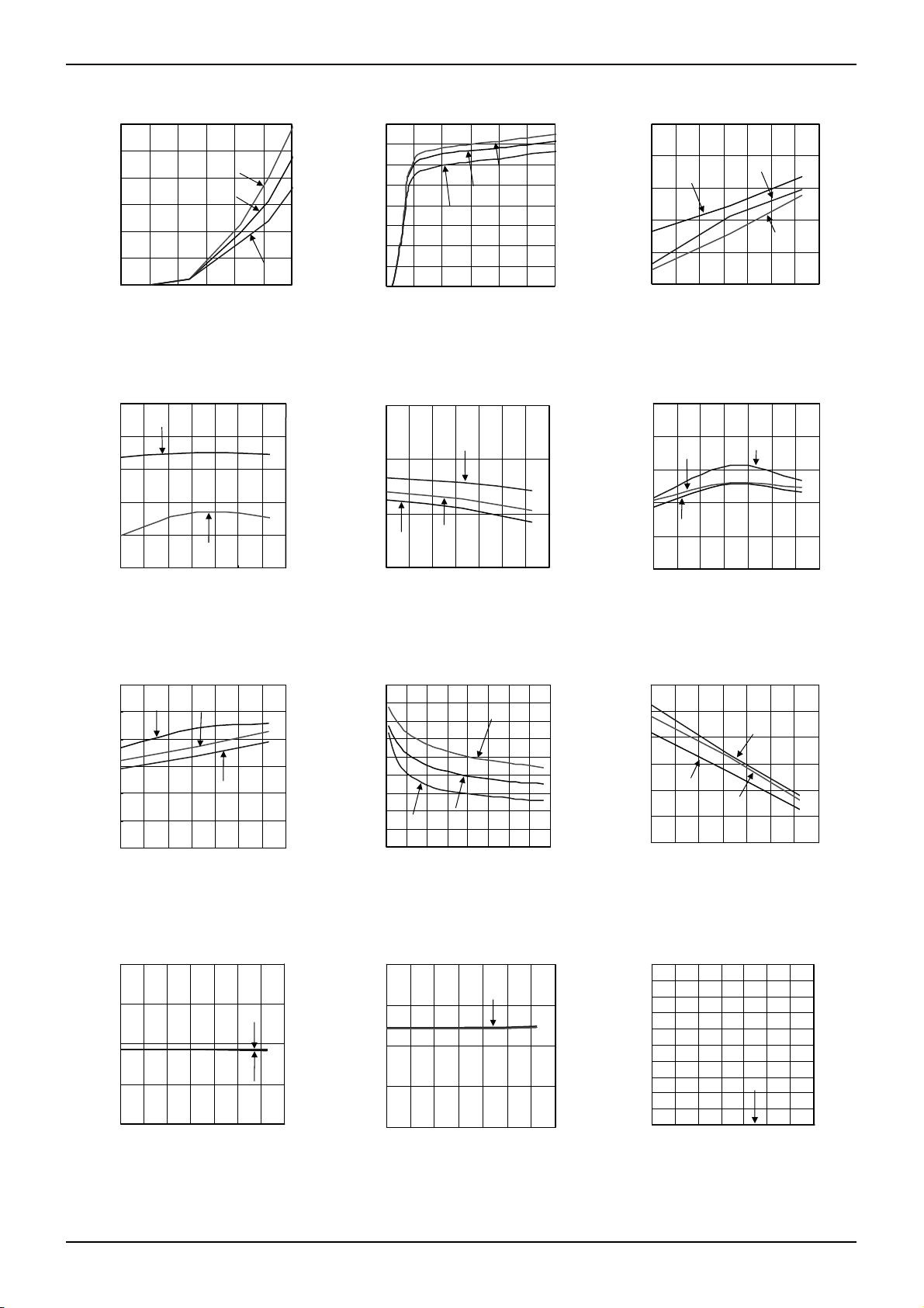
●Reference Data
30
25
20
15
ICC [uA]
10
5
0
0 5 10 15 20 25 30
Fig 1. Quiescent Current Fig 2. Current Consumption Fig 3. VREG Voltage
3.9
3.8
3.7
RISING
3.6
UVLO (V)
3.5
3.4
-40 -20 0 20 40 60 80 100
Fig 4. Under Voltage Lock Out
98
4.2V
97
96
95
Max D uty [%]
94
93
92
-40 - 20 0 20 40 60 80 100
Fig 7. Max Duty
1.2
1.1
1
VDET [V]
0.9
0.8
-40 - 20 0 20 40 60 80 100
Fig 10. Over Voltage Protect
25℃
VBAT [V]
FALLING
TEMP (°C)
5V
TEMP [℃]
TEMP [°C ]
85℃
6V
5V, 6V
4.2V
-40℃
4
3.5
3
2.5
2
ICC [mA]
1.5
1
0.5
0
0 5 10 15 20 25 30
620
610
ISET [mV]
600
4.2V
590
-40-200 20406080100
-40℃
5V
TEMP [°C ]
85℃
25℃
VBAT [V]
6V
Fig 5. ISET Voltage
900
800
700
600
500
400
RON [m]
300
200
-40℃
100
0
2.4 3 3.6 4.2 4.8 5.4 6 6. 6 7.2
85℃
25℃
VREG [V]
Fig 8. LX NcH RON
70
60
50
VDET [mV]
40
30
-40 - 20 0 20 40 60 80 100
4.2V, 5V, 6V
TEMP [℃]
Fig 11. SBD Open Protect
Technical Note
5.3
5.2
6V
5.1
5
VREG [V]
4.9
4.8
-40 -20 0 20 40 60 80 100
1500
1400
5V
1300
1200
FREQ [kHz]
1100
1000
4.2V
-40 - 20 0 20 40 60 80 100
Fig 6. Switching Frequency
2.6
2.4
2.2
2
1.8
SW_ICOIL [A]
1.6
1.4
4.2V
-40 -20 0 20 40 60 80 100
Fig 9. Over Current Limit
1
0.9
0.8
0.7
A]
0.6
µ
0.5
0.4
VDET [
0.3
0.2
0.1
0
VBAT=VREG=5V
-40 - 20 0 20 40 60 80 100
Fig 12. VDET Leak Current
22V
TEMP [℃]
6V
TEMP [℃]
6V
5V
TEMP [°C ]
TEMP [°C ]
12V
www.rohm.com
© 2011 ROHM Co., Ltd. All rights reserved.
3/28
2011.06 - Rev.B
BD6150MUV
50
45
40
ILED Max [m A]
35
30
34567
100
-40℃
90
80
70
Efficiency [%]
60
50
40
0102030
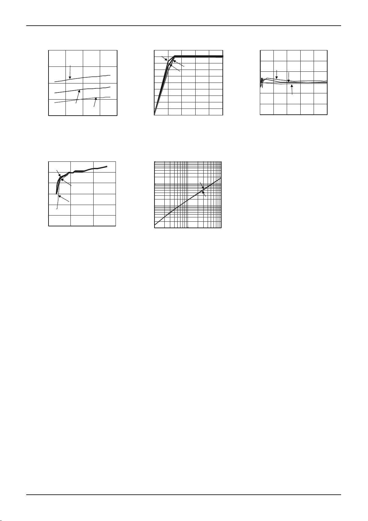
Fig 16. Efficiency
10LEDx6CH
-40℃
25℃
VBAT [V]
25℃
85℃
VBAT [V]
85℃
20
-40℃
18
16
14
12
10
ILED [mA]
8
6
4
2
0
0 0.2 0.4 0.6 0.8 1
85℃
25℃
VLED [V]
Fig 14. LED Current vs LED VoltageFig 13. LED Max Current
100
10
ILED [mA]
1
0.1
1 10 100
6V
12V, 26V
Duty [%]
Fig 17. LED Current vs PWM Duty
PWM Freq=200Hz LED 10x6CH
Technical Note
3
2
-40℃
1
0
-1
Mat chi ng [%]
-2
-3
0 20406080100
Fig 15. LED Current Matching
25℃
85℃
Duty [%]
www.rohm.com
© 2011 ROHM Co., Ltd. All rights reserved.
4/28
2011.06 - Rev.B
BD6150MUV
p
R
T
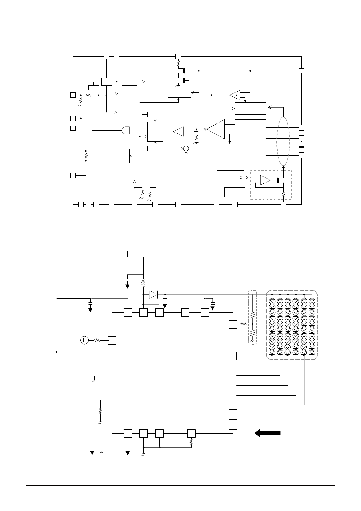
●Block diagram
PWMPOW
SW
SW
PGND
●Application example
2.2µF
Vin=2.1V to 5.5V
f
=100Hz~ 1kHz
PWM
PWM
VBAT VREG
REG
TSD
5.5V
Clam
Internal Power
Current SENCE
Over Current Protect
Internal Power
Supply
Control
UVLO
Internal Reset
Soft start
Control
SENCE
OSC
FSEL
FAIL FLAG
FAULT
DETECTO
PWM COMP
GND TEST OCPSET N.C. N.C. N.C.
Output Over Voltage PROTECT
+
SBD OPEN/
Output short PROTECT
ERRAMP
-
+
ISET
Resistor driver
PWMDRV ISET
LED TERMINAL
OPEN/SHORT
DETECTOR
LED
RETURN
SELECT
Fig.18 BD6150MUV block diagram
Battery or adapter
4.2V to 26V
1MΩ 26.7kΩ
10kΩ
PGND
10kΩ
68kΩ
4.7µH
SW SW
VREG
PWMPOW
PWMDRV
N.C.
TEST
FSEL
2.2µF
/ 50V
FAILFLAG
BD6150MUV
1µF
VDET
VBAT
N.C.
LED1
LED2
LED3
LED4
OCPSET
PGND
GND GND
ISET
LED5
LED6
N.C.
22kΩ
Fig.19 Application example (10LED × 6parallel, Switching frequency 750kHz)
Technical Note
6ch
+
-
Current Driver
GND
10LED × 6 parallel
19.6mA
VDE
LED1
LED2
LED3
LED4
LED5
LED6
www.rohm.com
© 2011 ROHM Co., Ltd. All rights reserved.
5/28
2011.06 - Rev.B
BD6150MUV
A
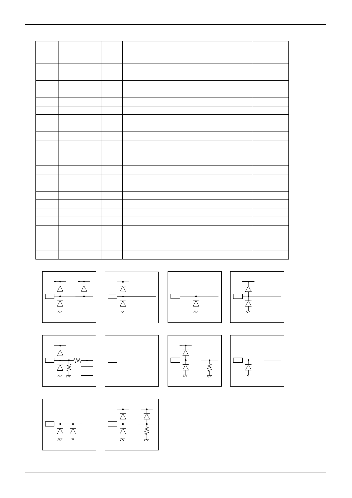
●Pin assignment table
PIN
No.
PIN Name
1 SW Out Switching Tr drive terminal H
2 SW Out Switching Tr drive terminal H
3 N.C. - No connect pin F
4 PGND - PGND for switching Tr D
5 FAILFLAG Out Fail Flag C
6 OCPSET In Current Limiter setting A
7 VDET In Detect input for SBD open and OVP A
8 TEST In TEST signal J
9 FSEL In Selection of Frequency, ‘L’: 1.25MHz, ‘H’: 0.75MHz J
10 ISET In Resister connection for LED current setting A
11 GND - GND for Switching Regulator B
12 N.C. In No connect pin F
13 LED1 In Current sink for LED C
14 LED2 In Current sink for LED C
15 LED3 In Current sink for LED C
16 LED4 In Current sink for LED C
17 LED5 In Current sink for LED C
18 LED6 In Current sink for LED C
19 N.C. In No connect pin F
20 GND - GND for Current driver B
21 PWMDRV In PWM input pin for power ON/OFF only driver G
22 VREG Out Regulator output / Internal power-supply D
23 PWMPOW In PWM input pin for power ON/OFF E
24 VBAT In Battery input I
VBAT
PIN
GND
VBAT
PIN
GND
E
PIN
GND
PGND
I
VREG
5.5V
Clump
In/
Out
PIN
PIN
PIN
VBAT
PGND
VBAT
GND
Technical Note
VBAT
GND
PGND
Terminal
D
H
diagram
Function
PIN
GND
VBAT
GND
C
G
B
PIN
F
VREG
J
PIN
PIN
www.rohm.com
© 2011 ROHM Co., Ltd. All rights reserved.
6/28
2011.06 - Rev.B
BD6150MUV
●Description of Functions
1) PWM current mode DC/DC converter
While this IC is power ON, the lowest voltage of LED terms is detected, PWM duty is decided to be 0.7V and output
voltage is kept invariably. As for the inputs of the PWM comparator as the feature of the PWM current mode, one is
overlapped with error components from the error amplifier, and the other is overlapped with a current sense signal that
controls the inductor current into Slope waveform to prevent sub harmonic oscillation. This output controls internal Nch
Tr via the RS latch. In the period where internal Nch Tr gate is ON, energy is accumulated in the external inductor, and in
the period where internal Nch Tr gate is OFF, energy is transferred to the output capacitor via external SBD.
This IC has many safety functions, and their detection signals stop switching operation at once.
2) Soft start
This IC has soft start function.
The soft start function prevents large coil current.
Rush current at turning on is prevented by the soft start function.
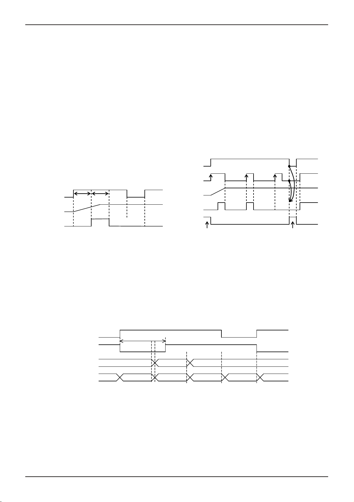
After PWMPOW, PWMDRV is changed L H, soft start becomes effective for within 4ms and soft start doesn't become
effective even if PWMPOW is changed L H after that.
And, when the H section of PWMPOW is within 4ms, soft start becomes invalid when PWMPOW is input to H more than
three times. The invalid of the soft start can be canceled by making PWMPOW, PWMDRV L.
Technical Note
PWMDRV
PWMPOW
PWMPOW
VREG
Soft start
3) FAILFLAG
When the error condition occurs, boost operating is stopped by the protection function, and the error condition is
outputted from FAILFLAG. After power ON, when the protection function is operating under about 1ms have passed.
Object of protect function is as shown below.
Max 1ms
Max 3ms
OFF ON
OFF
OFF
Soft start
Soft start
reset
OFF ON ON OFF OFF OFF ON
Reset Reset
Fig.20 Soft start Fig.21 Soft start reset and set
・Over-voltage protection
・External SBD open detect/ Output Short protection
・LED terminal open/short protection
・Over current limit
VREG
PWMPOW
FAI LFL AG
about 1ms
Protection
function
un-detection detect un-detection
Boost
operating
off
normal boost stop normal off normal
Fig.22 FAILFLAG operating description
OFF OFF
www.rohm.com
© 2011 ROHM Co., Ltd. All rights reserved.
7/28
2011.06 - Rev.B
BD6150MUV
t
k
V
●Protection
・Over voltage protection
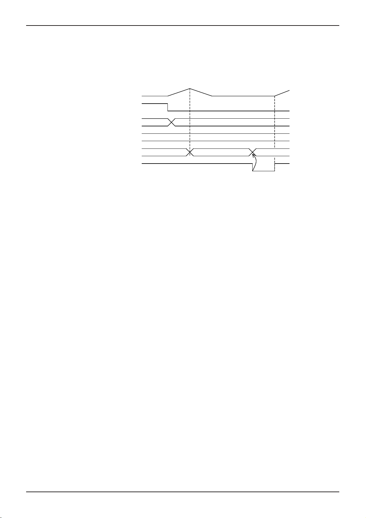
At such an error of output open as the output DC/DC and the LED is not connected to IC, the DC/DC will boost too much
and the VDET terminal exceed the absolute maximum ratings, and may destruct the IC. Therefore, when VDET becomes
sensing voltage or higher, the over voltage limit works, and turns off the output Tr, and the pressure up made stop.
At this moment, the IC changes from activation into non-activation, and the output voltage goes down slowly. And, when
the Feedback of LED1 isn’t returned, so that Vout will return normal voltage.
Technical Note
Vou
LED1 voltage
LED1 connection
normal
LED2 connection
LED1 FeedBac
return return off
PWMPOW, PWMDR
Fig.23 VDET operating description
・External SBD open detect / Output short protection
In the case of external SBD is not connected to IC, or VOUT is shorted to GND, the coil or internal Tr may be destructed.
Therefore, at such an error as VDET becoming 0.05V or below, and turns off the output Tr, and prevents the coil and the IC
from being destructed.
And the IC changes from activation into non-activation, and current does not flow to the coil (0mA).
・Thermal shut down
This IC has thermal shut down function.
The thermal shut down works at 175℃ or higher, and the IC changes from activation into non-activation.
open
normal
www.rohm.com
© 2011 ROHM Co., Ltd. All rights reserved.
8/28
2011.06 - Rev.B
BD6150MUV
Technical Note
●How to set over voltage limit
This section is especially mentioned here because the spec shown electrical characteristic is necessary to explain this
section.
Over voltage limit min 0.96V typ 1.00V max 1.04V
LED control voltage min 0.56V typ 0.70V max 0.84V
LED terminal over voltage protect min 10.0V typ 11.5 V max 13.0V
1. Calculate the conditions that the total value of LED VF is MAX.
Example) In the case of serial 8 LEDs with VF=2.9V(min), 3.2V(typ), 3.5V(max) => 3.5V x 8=28V
2. Then calculate the biggest value of output with the following formula.
The biggest value of output = the biggest value calculated for 1 + the biggest value of LED terminal voltage. (0.84V)
Example) The biggest value of output = 28V + 0.84V =28.84V
3. Set the smallest value of over voltage larger than the biggest value of output.
If over voltage is closer to the total value of VF, it could be occurred to detect over voltage by ripple, noise, and so on.
It is recommended that some margins should be left on the difference between over voltage and the total value of VF.
This time around 6% margin is placed.
Example) Against the biggest value of output = 28.84V, the smallest value of over voltage = 28.84V x 1.06 = 30.57V
Ic over voltage limit min=0.96V,typ=1.00V, max=1.04V
typ = 30.57V×(1.00V/0.96V) = 31.8V
max = 31.8V×(1.04V/1.00V) = 33.1V
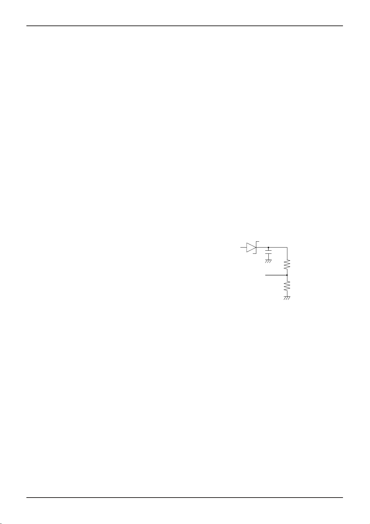
4. The below shows how to control resistor setting over voltage
Please fix resistor 2.2MΩ between VDET and output and then set over voltage after changing resistor between VDET
and GND. While PWM is off, output voltage decreases by minimizing this resistor. Due to the decrease of output voltage,
ripple of output voltage increases, and singing of output condenser also becomes bigger.
Example) Selecting OVP resistor.
(Example 1) VF=3.6V max, serial = 7 LED
OVP = 1.0V, R1 = 2.2M, R2 = 78.7k
VOUT = 1.0 × (2.2M + 78.7k)/ 78.7k = 28.95V
VOUT
(Example 2) VF=3.6V max, serial = 8 LED
OVP = 1.0V, R1 = 2.2M, R2 = 69.8k
VOUT = 1.0 × (2.2M + 69.8k)/ 69.8k = 32.52
(Example 3) VF=3.6V max, serial = 9 LED
VDET
R1
OVP = 1.0V, R1 = 2.2M, R2 = 62k
VOUT = 1.0 × (2.2M + 62k)/ 62k = 36.48V
R2
(Example 4) VF=3.6V max, serial = 10 LED
OVP = 1.0V, R1 = 1.0M, R2 = 26.7k
VOUT = 1.0 × (1.0M + 26.7k)/ 26.7k =
38.45V
5. The following shows how to confirm if LEDs are not turned on while selecting terminals. If the difference between the
VF’s total value of LED and over voltage is less than min.10V of LED terminal over voltage protect, LEDs should be
turned on.
LEDs are turned on, as the following formula shows; 33.1V-2.9V x 8 serial = 9.9V<10.0V.
www.rohm.com
© 2011 ROHM Co., Ltd. All rights reserved.
9/28
2011.06 - Rev.B
 Loading...