


A
LED Driver s for LCD Backlights
Mulitifunction Backlight LED Driver
for Small LCD Panels (Charge Pump Type)
BD6088GUL
●Description
BD6088GUL is “Intelligent LED Driver” that is the most suitable for the cellular phone.
It has 6LED driver for LCD Backlight and GPO 4 port.
It has ALC function, that is “Low Power Consumption System” realized.
It can be developed widely from the model high End to the model Low End.
As it has charge pump circuit for DCDC, it is no need to use coils, and it contributes to small space.
VCSP50L3(3.50mm×3.50mm 0.5mm space)
It adopts the very thin CSP package that is the most suitable for the slim phone.
●Functions
1) Total 6LEDs driver for LCD Backlight
It have 4LEDs (it can select 4LED or 3LED) for exclusire use of Main and 2LEDs which can
chose independent control or a main allotmert by resister setting.
“Main Group” can be controlled by Auto Luminous Control (ALC) system.
“Main Group” can be controlled by external PWM signal.
ON/ off and a setup of electric current are possible at the time of the independent control by the independence.
2) Ambient Light sensor interface
Main backlight can be controlled by ambient brightness.
Photo Diode, Photo Transistor, Photo IC(Linear/Logarithm) can be connected.
Bias source for ambient light sensor, gain and offset adjustment are built in.
LED driver current as ambient level can be customized.
3) Charge Pump DC/DC for LED driver
It has x1/x1.5/ x2 mode that will be selected automatically.
The most suitable voltage up magnification is controlled automatically by LED port voltage.
Output voltage fixed mode function loading (3.9V/4.2V/4.5V/4.8V)
Soft start
4) GPO 4 Port
Open Drain output and slope control loading
5) Thermal shutdown
6) I2C BUS FS mode(max 400kHz)
*This chip is not designed to protect itself against radioactive rays.
*This material may be changed on its way to designing.
*This material is not the official specification.
●Absolute Maximum Ratings (Ta=25 oC)
functions, Over voltage protec t i on (Auto-return t ype), Over current protection (Auto-return t ype) Loading
No.11040EAT29
Parameter Symbol Ratings Unit
Maximum voltage VMAX 7 V
Power Dissipation Pd 1380
Operating Temperature Range Topr -30 ~ +85 ℃
Storage Temperature Range Tstg -55 ~ +150 ℃
note) Power dissipation deleting is 11.04mW/ oC, when it’s used in over 25 oC.
(It’s deleting is on the board that is ROHM’s standard)
●Operating conditions (VBAT≥VIO, Ta=-35~85
Parameter Symbol Ratings Unit
VBAT input voltage VBAT 2.7 ~ 5.5 V
VIO pin voltage VIO 1.65 ~ 3.3 V
www.rohm.com
© 2011 ROHM Co., Ltd. All rights reserved.
(note
mW
o
C)
1/51
2011.04 - Rev.

A
BD6088GUL
●Electrical Characteristics (Unless otherwise specified, Ta=25°C, VBAT=3.6V, VIO=2.6V)
Parameter Symbol
【Circuit Current】
VBAT Circuit current 1 IBAT1 - 0.1 3.0 μA RESETB=0V, VIO= 0V
VBAT Circuit current 2 IBAT2 - 0.5 3.0 μA RESETB=0V, VIO=2.6V
Min. Typ. Max.
Limits
Unit Condition
Technical Note
VBAT Circuit current 3 IBAT3 - 61 65 mA
VBAT Circuit current 4 IBAT4 - 92 102 mA
VBAT Circuit current 5 IBAT5 - 123 140 mA
VBAT Circuit current 6 IBAT6 - 0.25 1.0 mA
【LED Driver】
LED current Step (Setup) ILEDSTP1 128 Step LED1~6
LED current Step (At slope) ILEDSTP2 256 Step LED1~6
LED Maximum setup current IMAXWLED - 25.6 - mA LED1~6
LED current accuracy IWLED -7% 15 +7% mA I
LED current Matching ILEDMT - - 4 %
LED OFF Leak current ILKLED - - 1.0 μA VLED=4.5V
【DC/DC(Charge Pump)】
Output Voltage 1 VoCP1 - Vf+0.2 Vf+0.25 V Vf is forward direction of LED
3.705 3.9 4.095 V
Output Voltage 2 VoCP2
3.99 4.2 4.41 V
4.275 4.5 4.725 V
4.56 4.8 5.04 V
DC/DC x1 mode, Io=60mA
VBAT=4.0V
DC/DC x1.5 mode, Io=60mA
VBAT=3.6V
DC/DC x2 mode, Io=60mA
VBAT=2.7V
ALC Operating
ALCEN=1, AD cycle=0.5s setting
Except sensor current
=15mA setting, VLED=1.0V
LED
Between LED1~6
at VLED=1.0V, ILED=15mA
Fixation Voltage Output
ModeIo=60mA
VBAT≧3.2V
Drive ability IOUT - - 150 mA VBAT≥3.2V, VOUT=3.9V
Switching frequency fosc 0.8 1.0 1.2 MHz
Over Voltage
Protection detect voltage
Over Current
Protection detect Current
【Sensor Interface】
SBIAS Output Voltage VoS
SBIAS Maximum Output current IomaxS 30 - - mA Vo=2.6V setting
SBIAS Discharge resister at OFF ROFF S - 1.0 1.5 kΩ
SSENS Input range VISS 0 -
ADC resolution ADRES 8 bit
ADC integral calculus non-linearity ADINL -3 - +3 LSB
ADC differential calculus
non-linearity
OVP - 6.0 6.5 V
OCP - 250 375 mA VOUT=0V
2.85 3.0 3.15 V Io=200µA
2.47 2.6 2.73 V Io=200µA
VoS×
255/256
ADDNL -1 - +1 LSB
V
www.rohm.com
© 2011 ROHM Co., Ltd. All rights reserved.
2/51
2011.04 - Rev.

A
BD6088GUL
●Electrical Characteristics (Unless otherwise specified, Ta=25°C, VBAT=3.6V, VIO=2.6V)
Parameter Symbol
【SDA, SCL】 (I2C Interface)
L level input voltage VILI -0.3 -
H level input voltage VIHI
Hysteresis of Schmitt trigger input VhysI
L level output voltage VOLI 0 - 0.3 V SDA Pin, IOL=3 mA
Min. Typ. Max.
0.75 ×
VIO
0.05 ×
VIO
Limits
0.25 ×
VIO
VBAT
-
+0.3
- - V
Unit Condition
V
V
Technical Note
Input current linI - - 1 μA
【RESETB】 (CMOS Input Pin)
L level input voltage VILR -0.3 -
H level input voltage VIHR
Input current IinR - - 1 μA
【WPWMIN】 (NMOS Input Pin)
L level input voltage VILA -0.3 - 0.3 V
H level input voltage VIHA 1.4 -
Input Current IinA - - 1 μA
PWM input minimum High pulse
width
【OUTCNT】 (Pull-down resistance NMOS Input Pin)
L level input voltage VILA -0.3 - 0.3 V
H level input voltage VIHA 1.4 -
Input Current IinA - 3.6 10 μA Vin=1.8V
PWmin 80 - - μs WPWMIN Pin
0.75 ×
VIO
0.25 ×
VIO
VBAT
-
+0.3
VBAT
+0.3
VBAT
+0.3
Input Voltage
= 0.1×VIO~0.9×VIO
V
V
Input Voltage
= 0.1×VIO~0.9×VIO
V
Input Voltage
= 0.1×VBAT~0.9×VBAT
V
【OUT1~4】 ( NMOS Open Drain Outp ut Pin)
L level output voltage VOLG - - 0.3 V IOL=10mA
Output Leak current ILKG - - 1.0 μA Vout=3.6V
【GC1, GC2】 (Sensor Gain Control CMOS Output Pin)
L level output voltage VOLS - - 0.2 V IOL=1mA
H level output voltage VOHS
【KBLT】 (Key Back Light Control CMOS Output Pin)
L level output voltage VOLK - - 0.2 V IOL=1mA
H level output voltage VOHK
Pull-downregistance RPUDK - 1.0 2.0 MΩ Vin=3.3V
VoS
-0.2
VIO
-0.2
- - V IOH=1mA
- - V IOH=1mA
www.rohm.com
© 2011 ROHM Co., Ltd. All rights reserved.
3/51
2011.04 - Rev.
A
BD6088GUL
A
( ) ( )
( )
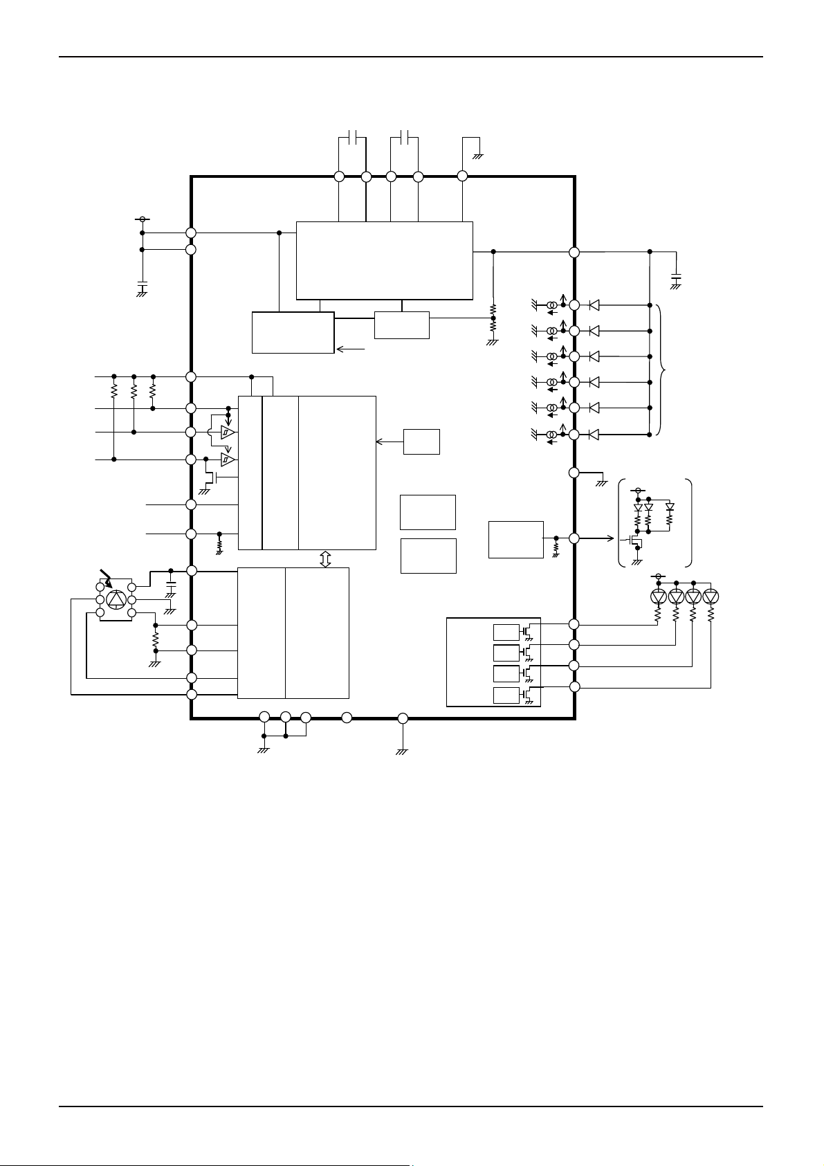
●Block Diagram / Application Circuit example 1
1μF
Technical Note
1μF
GC1
GC2
Photo IC
BH1600FVC
VBAT
VDD
GND
IOUT
10µF
VBATCP
VBAT1
VIO
RESETB
SCL
SD
WPWMIN
OUTCNT
SBIAS
SSENS
SGND
GC2
GC1
1μF
Charge Pump
Mode Control
Level
I/O
Sensor
I/F
Shift
ALC
C1P
C1N
Charge Pump
x1 / x1.5 / x2
LED terminal voltage feedback
I2C interface
Digital Control
LED
control
C2N
OVP
C2P
TSD
IREF
VREF
CPGND
GPO
Key
Control
Slope
Control
Slope
Control
Slope
Control
Slope
Control
VOUT
LED1
LED2
LED3
LED4
LED5
LED6
LEDGND
KBLT
OUT1
OUT2
OUT3
OUT4
VBAT
・・
VBAT
Key Pad
LED
1μF
Main Back Light
www.rohm.com
© 2011 ROHM Co., Ltd. All rights reserved.
T4
T1
T2
T3
(Open)
GND1
Fig.1 Block Diagram / Application Circuit example 1
4/51
2011.04 - Rev.
A
BD6088GUL
A
( )
( )
( )
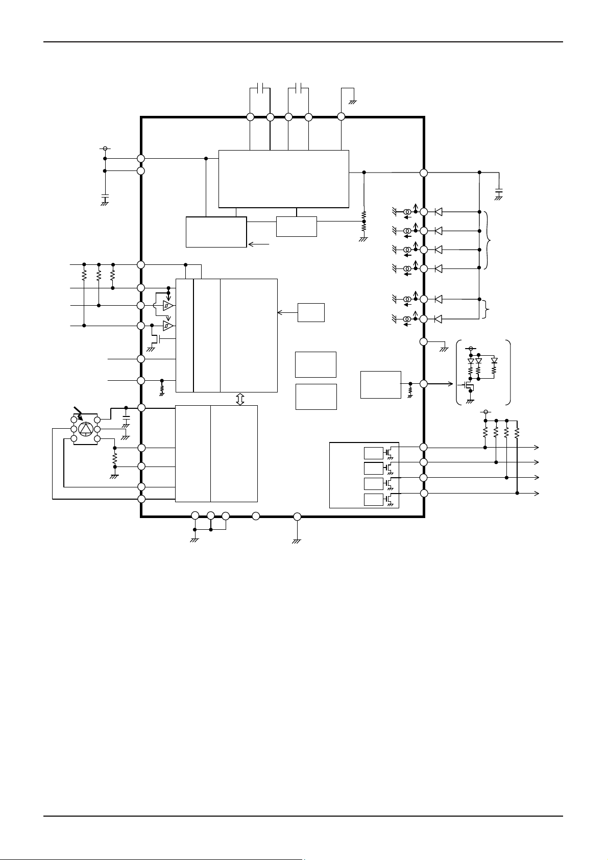
●Block Diagram / Application Circuit example 2
1μF
Technical Note
1μF
GC1
GC2
Photo IC
BH1600FVC
VBAT
VDD
GND
IOUT
10µF
VBATCP
VBAT1
VIO
RESETB
SCL
SD
WPWMIN
OUTCNT
SBIAS
SSENS
SGND
GC2
GC1
1μF
Charge Pump
Mode Control
Level
I/O
Sensor
I/F
Shift
ALC
C1P
C1N
Charge Pump
x1 / x1.5 / x2
LED terminal voltage feedback
I2C interface
Digital Control
LED
control
C2N
OVP
C2P
TSD
IREF
VREF
CPGND
GPO
Key
Control
Slope
Control
Slope
Control
Slope
Control
Slope
Control
VOUT
LED1
LED2
LED3
LED4
LED5
LED6
LEDGND
KBLT
OUT1
OUT2
OUT3
OUT4
VBAT
・・
VBAT
Key Pad
LED
2ch
Sub Back Light
1μF
4ch
Main Back Light
T4
T1
T2
T3
(Open)
GND1
Fig.2 Block Diagram / Application Circuit example 2
www.rohm.com
© 2011 ROHM Co., Ltd. All rights reserved.
5/51
2011.04 - Rev.

A
BD6088GUL
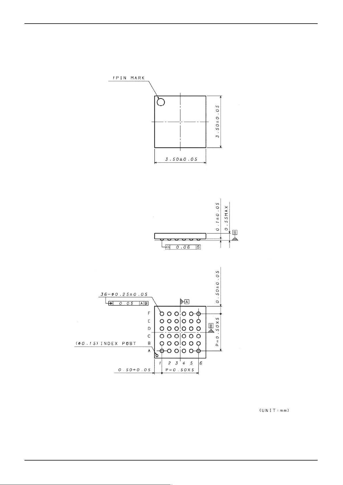
●Pin Arrangement [Bottom View]
F
E
D
C
T3
T4 SSENS SGND VBAT1 VIO
SBIAS GC1 GC2 SDA OUT2 OUT4
LED5 LED6 SCL OUT1 OUT3 VOUT
LEDGND LED4 OUTCNT WPWMIN C1P C2P
Technical Note
6 x 6 Ball
B
A
INDEX
○
LED2 LED3 RESETB KBLT C2N VBATCP
T1 LED1 GND1 C1N CPGND T2
1 2 3 4 5 6
www.rohm.com
© 2011 ROHM Co., Ltd. All rights reserved.
6/51
2011.04 - Rev.
A
BD6088GUL
●Package
VCSP50L3 CSP small package
SIZE : 3.50mm×3.50mm(A difference in public:X,Y Both ±0.05mm) Height : 0.55mm max
A ball pitch : 0.5 mm
2
Technical Note
www.rohm.com
© 2011 ROHM Co., Ltd. All rights reserved.
7/51
2011.04 - Rev.

A
BD6088GUL
●Pin Functions
No Ball No. Pin Name I/O
1 B6 VBATCP - - GND Battery is connected A
2 F4 VBAT1 - - GND Battery is connected A
3 A1 T1 I VBAT - Test Ground Pin(short to Ground) B
4 A6 T2 I VBAT GND Test Input Pin (short to Ground) S
5 F6 T3 O VBAT GND Test Output Pin(Open) M
6 F1 T4 I VBAT GND Test Input Pin (short to Ground) S
7 F5 VIO - VBAT GND I/O Power supply is connected C
8 B3 RESETB I VBAT GND Reset input (L: reset, H: reset cancel) H
9 E4 SDA I/O VBAT GND I2C data input / output I
10 D3 SCL I VBAT GND I2C clock input H
11 A5 CPGND - VBAT 12 A3 GND1 - VBAT 13 C1 LEDGND - VBAT 14 A4 C1N I/O VBAT GND
15 C5 C1P I/O - GND
16 B5 C2N I/O VBAT GND
17 C6 C2P I/O - GND
18 D6 VOUT O - GND Charge Pump output pin A
19 A2 LED1 I - GND LED is connected 1 for LCD Back Light E
20 B1 LED2 I - GND
21 B2 LED3 I - GND
22 C2 LED4 I - GND
23 D1 LED5 I - GND
24 D2 LED6 I - GND
25 E1 SBIAS O VBAT GND Bias output for the Ambient Light Sensor Q
26 F2 SSENS I VBAT GND Ambient Light Sensor input N
27 E2 GC1 O VBAT GND Ambient Light Sensor gain control output 1 X
28 E3 GC2 O VBAT GND Ambient Light Sensor gain control output 2 X
29 F3 SGND - VBAT - Ground B
30 D4 OUT1 O - GND General Output Port 1 U
31 E5 OUT2 O - GND General Output Port 1 U
32 D5 OUT3 O - GND General Output Port 1 U
33 E6 OUT4 O - GND General Output Port 1 U
34 C4 WPWMIN I VBAT GND External PWM input for Back Light * V
35 C3 OUTCNT I VBAT GND OUT1,2,3,4 Output Control (L:OFF) * L
36 B4 KBLT O VBAT GND Key Back Light Control Output W
* A setup of a register is separately necessary to make it effective.
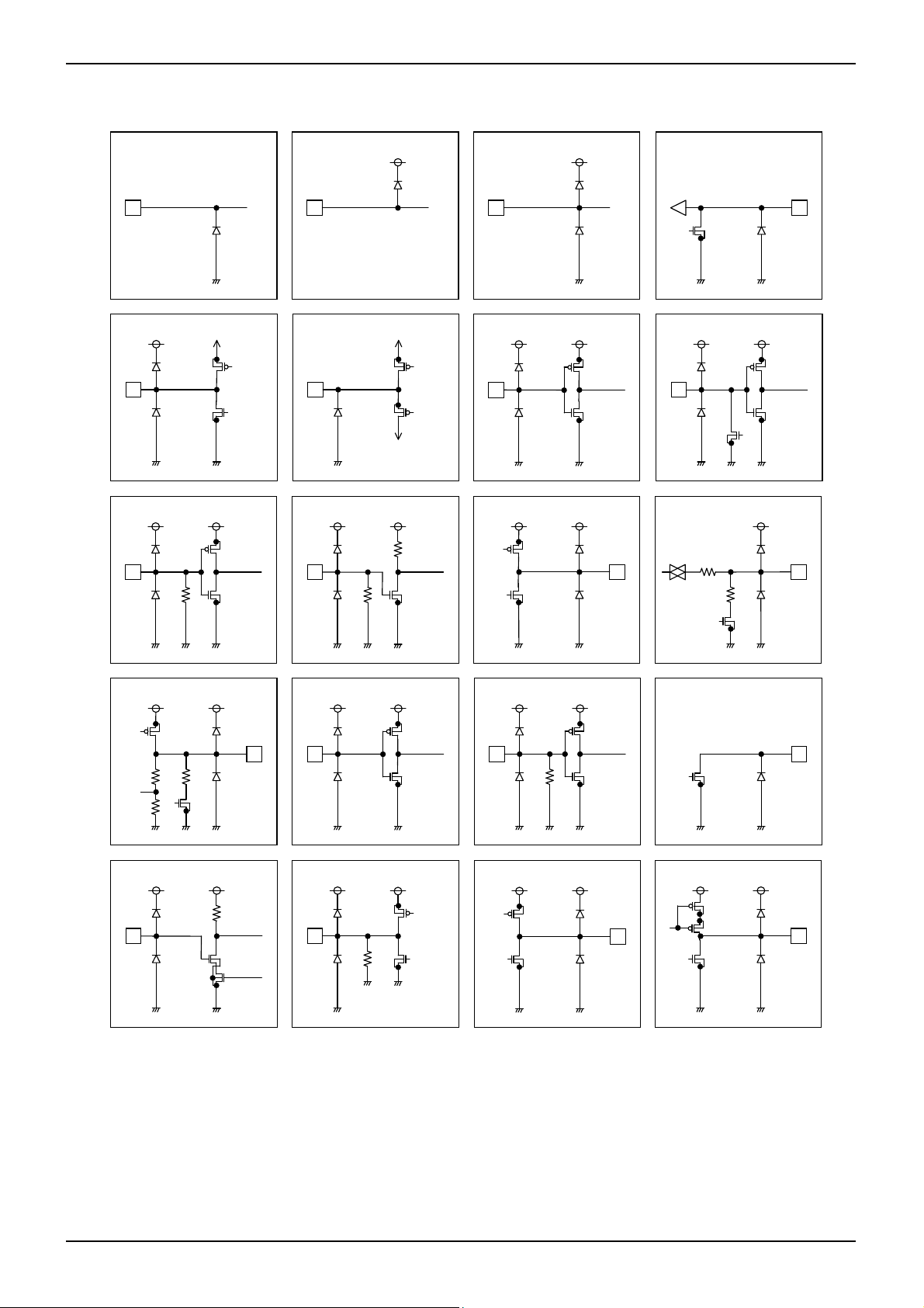
ESD Diode
For Power For Ground
Functions
Ground
Ground
Ground
Charge Pump capacitor is connected
Charge Pump capacitor is connected
Charge Pump capacitor is connected
Charge Pump capacitor is connected
LED is connected 2 for LCD Back Light
LED is connected 3 for LCD Back Light
LED is connected 4 for LCD Back Light
LED is connected 5 for LCD Back Light
LED is connected 6 for LCD Back Light
Technical Note
Equivalent
Circuit
B
B
B
F
G
F
G
E
E
E
E
E
www.rohm.com
© 2011 ROHM Co., Ltd. All rights reserved.
8/51
2011.04 - Rev.
A
BD6088GUL
●Equivalent Circuit
A VBATB E
C
Technical Note
VBAT
F
VBAT
J
Q
VBAT VBAT
G
VIO VBAT
R
VBATVBAT L
VBATVBAT
H
M
VBAT VBAT
S
VIOVBAT
VBATVBAT
I
N
U
VIOVBAT
VBAT
VBAT VBAT V
www.rohm.com
© 2011 ROHM Co., Ltd. All rights reserved.
VBAT W
VIO
X
VoS VBAT
9/51
Y
VIO VBAT
2011.04 - Rev.
A
BD6088GUL
Technical Note
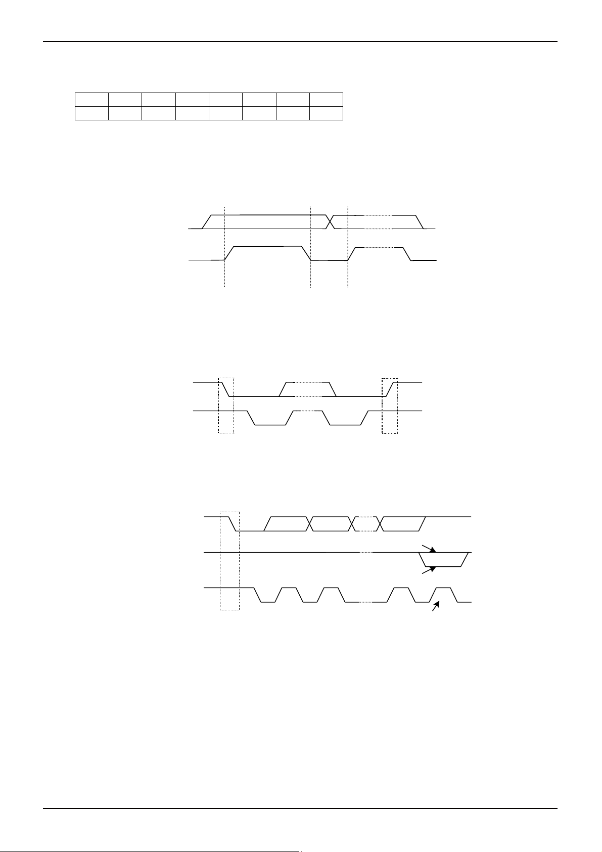
●I2C BUS format
The writing/reading operation is based on the I
2
C slave standard.
・Slave address
A7 A6 A5 A4 A3 A2 A1 R/W
1 1 1 0 1 1 0 1/0
・Bit Transfer
SCL transfers 1-bit data during H. SCL cannot change signal of SDA during H at the time of bit transfer. If SDA changes
while SCL is H, START conditions or STOP conditions will occur and it will be interpreted as a control signal.
SDA
SCL
SDA a state of stability
Data are effective
SDA
:
It can change
・START and STOP condition
When SDA and SCL are H, data is not transferred on the I
2
C- bus. This condition indicates, if SDA changes from H to L
while SCL has been H, it will become START (S) conditions, and an access start, if SDA changes from L to H while SCL
has been H, it will become STOP (P) conditions and an access end.
SDA
SCL
S P
START condition
STOP condition
・Acknowledge
It transfers data 8 bits each after the occurrence of START condition. A transmitter opens SDA after transfer 8bits data, and
a receiver returns the acknowledge signal by setting SDA to L.
DATA OUTPUT
BY TRANSMITTER
DATA OUTPUT
BY RECEIVER
SCL
START condition
S
12 89
not acknowledge
acknowledge
clock pulse for
acknowledgement
www.rohm.com
© 2011 ROHM Co., Ltd. All rights reserved.
10/51
2011.04 - Rev.
A
BD6088GUL
A A
A
A
A7 A6 A5A4A3A2A1A
A
A
A
A
A
A
A
A A
A
A
A6A5A4A3A2A1A
A
A
A
A
Technical Note
・Writing protocol
A register address is transferred by the next 1 byte that transferred the slave address and the write-in command. The 3rd
byte writes data in the internal register written in by the 2nd byte, and after 4th byte or, the increment of register address is
carried out automatically. However, when a register address turns into the last address, it is set to 00h by the next
transmission. After the transmission end, the increment of the address is carried out.
*1 *1
D7 D6D5 D4D3 D2D1 D0 D7 D6 D5 D4 D3 D2D1 D0
X X X X X X X
S
R/W=0(write)
from master to slave
from slave to master
register addressslave address
00
DATA
register address
increment
=acknowledge(SDA LOW)
=not acknowledge(SDA HIGH)
S=START condition
P=STOP condition
*1: Write Timing
DATA
register address
・Reading protocol
It reads from the next byte after writing a slave address and R/W bit. The register to read considers as the following address
accessed at the end, and the data of the address that carried out the increment is read after it. If an address turns into the
last address, the next byte will read out 00h. After the transmission end, the increment of the address is carried out.
X X X X X X X
R/W=1(read)
from master to slave
from slave to master
P
D7 D6 D5 D4 D3 D2 D1 D0 D7 D6 D5 D4 D3 D2 D1 D0
DATA
register address
increment
=acknowledge(SDA LOW)
=not acknowledge(SDA HIGH)
S=START condition
P=STOP condition
DATA slave address
register address
increment
1 S
・Multiple reading protocols
After specifying an internal address, it reads by repeated START condition and changing the data transfer direction. The
data of the address that carried out the increment is read after it. If an address turns into the last address, the next byte will
read out 00h. After the transmission end, the increment of the address is carried out.
P
increment
S
slave address
R/W=0(write)
from master to slave
from slave to master
0
7
register address
D7 D6 D5 D4 D3D2D1D0 D7D6D5D4D3D2D1D0
DATA DATA
register address
increment
Sr 1
0X X X X X X X
X X X X X X X
slave address
=acknowledge(SDA LOW)
=not acknowledge(SDA HIGH)
S=START condition
P=STOP condition
Sr=repeated START condition
R/W=1(read)
P
register address
increment
As for reading protocol and mul tiple reading protocols, please do A(not acknowledge) after doing the final reading operation.
It stops with read when ending by A(acknowledge), and SDA stops in the state of Low when the readingdata of that time is
0. However, this state returns usually when SCL is moved, data is read, and A(not acknowledge)is done.
www.rohm.com
© 2011 ROHM Co., Ltd. All rights reserved.
11/51
2011.04 - Rev.
A
BD6088GUL
S
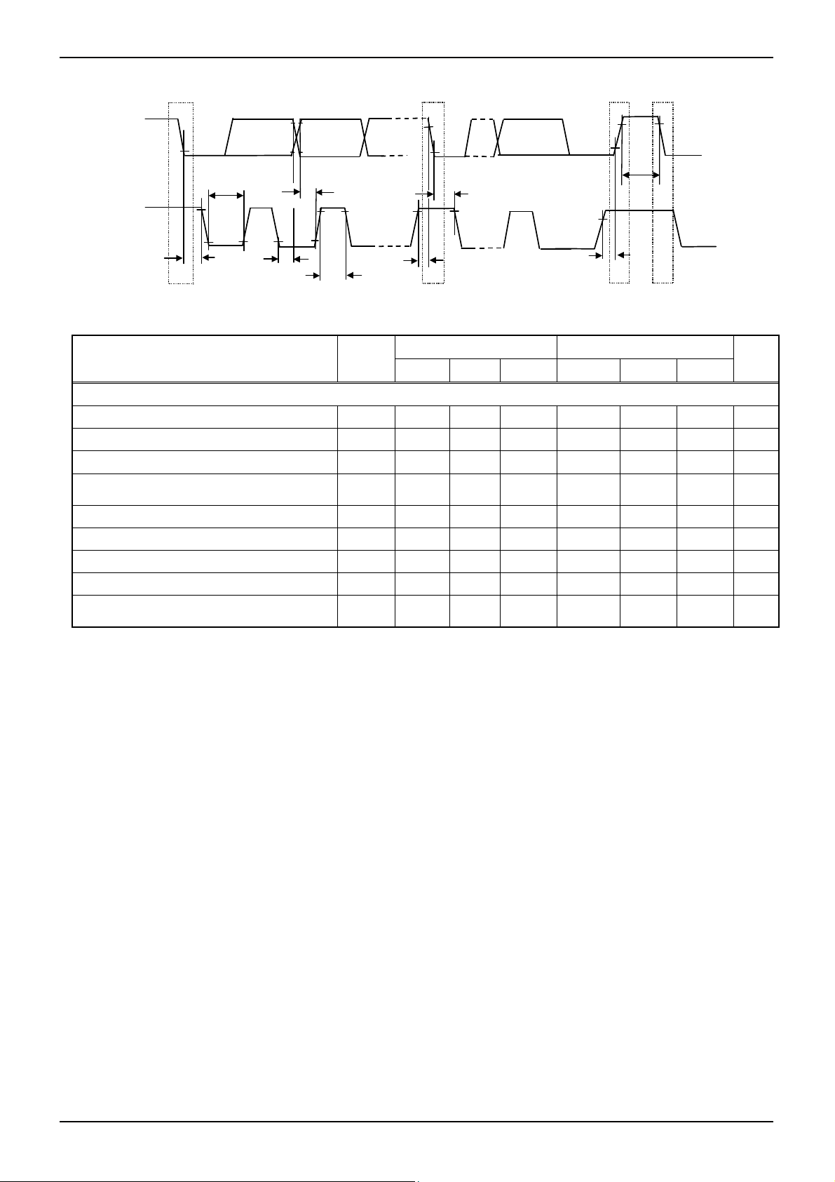
●Timing diagram
SDA
CL
t
LOW
SU;DAT
t
HD;STA
t
Technical Note
t BUF
SU;STA
t
HD;STA
t
HD;DAT
S Sr P
t
HIGH
t
t SU;STO
S
●Electrical Characteristics(Unless otherwise specified, Ta=25
o
C, VBAT=3.6V, VIO=2.6V)
Standard-mode Fast-mode
Parameter Symbol
Unit
Min. Typ. Max. Min. Typ. Max.
2
【I
C BUS format】
SCL clock frequency fSCL 0 - 100 0 - 400 kHz
LOW period of the SCL clock tLOW 4.7 - - 1.3 - - μs
HIGH period of the SCL clock tHIGH 4.0 - - 0.6 - - μs
Hold time (repeated) START condition
After this period, the first clock is generated
tHD;STA 4.0 - - 0.6 - - μs
Set-up time for a repeated START condition tSU;STA 4.7 - - 0.6 - - μs
Data hold time tHD;DAT 0 - 3.45 0 - 0.9 μs
Data set-up time tSU;DAT 250 - - 100 - - ns
Set-up time for STOP condition tSU;STO 4.0 - - 0.6 - - μs
Bus free time between a STOP and START
condition
t
BUF 4.7 - - 1.3 - - μs
www.rohm.com
© 2011 ROHM Co., Ltd. All rights reserved.
12/51
2011.04 - Rev.

A
BD6088GUL
●Register List
Address W/R
Register data
D7 D6 D5 D4 D3 D2 D1 D0
Technical Note
Function
00h W VOUT(1) VOUT(0) DCDCMD DCDCFON - - - SFTRST
01h W WPWMEN W PWMPOL - - W6MD W5MD W4MD MLEDMD LED Pin function setting
02h W/R - - - - ALCEN W6EN W5EN MLEDEN
03h W - IMLED(6) IMLED(5) IMLED(4) IMLED(3) IMLED(2) IMLED(1) IMLED(0)
04h W - IW5(6) IW5(5) IW5(4) IW5(3) IW5(2) IW5(1) IW5(0)
05h W - IW6(6) IW6(5) IW6(4) IW6(3) IW6(2) IW6(1) IW6(0)
06h W THL (3) THL (2) THL (1) THL (0) TLH (3) TLH (2) TLH (1) TLH (0)
07h W ADCYC (1) ADCYC (0) GAIN (1) GAIN(0) STYPE VSB MDCIR SBIASON
08h W SOFS (3) SOFS (2) SOFS (1) SOFS (0) SGAIN (3) SGAIN (2) SGAIN (1) SGAIN (0)
09h R - - - - AMB (3) AMB (2) AMB (1) AMB (0) Ambient level
0Ah W - IU0 (6) IU0 (5) IU0 (4) IU0 (3) IU0 (2) IU0 (1) IU0 (0) LED Current at Ambient level 0h
0Bh W - IU1 (6) IU1 (5) IU1 (4) IU1 (3) IU1 (2) IU1 (1) IU1 (0) LED Current at Ambient level 1h
0Ch W - IU2 (6) IU2 (5) IU2 (4) IU2 (3) IU2 (2) IU2 (1) IU2 (0) LED Current at Ambient level 2h
0Dh W - IU3 (6) IU3 (5) IU3 (4) IU3 (3) IU3 (2) IU3 (1) IU3 (0) LED Current at Ambient level 3h
0Eh W - IU4 (6) IU4 (5) IU4 (4) IU4 (3) IU4 (2) IU4 (1) IU4 (0) LED Current at Ambient level 4h
Software Reset
DC/DC function setting
Power Control
Main group current setting
LED5 current setting
LED6 current setting
Main Current transition
Measurement mode setting
Measurement data adjustment
0Fh W - IU5 (6) IU5 (5) IU5 (4) IU5 (3) IU5 (2) IU5 (1) IU5 (0) LED Current at Ambient level 5h
10h W - IU6 (6) IU6 (5) IU6 (4) IU6 (3) IU6 (2) IU6 (1) IU6 (0) LED Current at Ambient level 6h
11h W - IU7 (6) IU7 (5) IU7 (4) IU7 (3) IU7 (2) IU7 (1) IU7 (0) LED Current at Ambient level 7h
12h W - IU8 (6) IU8 (5) IU8 (4) IU8 (3) IU8 (2) IU8 (1) IU8 (0) LED Current at Ambient level 8h
13h W - IU9 (6) IU9 (5) IU9 (4) IU9 (3) IU9 (2) IU9 (1) IU9 (0) LED Current at Ambient level 9h
14h W - IUA (6) IUA (5) IUA (4) IUA (3) IUA (2) IUA (1) IUA (0) LED Current at Ambient level Ah
15h W - IUB (6) IUB (5) IUB (4) IUB (3) IUB (2) IUB (1) IUB (0) LED Current at Ambient level Bh
16h W - IUC (6) IUC (5) IUC (4) IUC (3) IUC (2) IUC (1) IUC (0) LED Current at Ambient level Ch
17h W - IUD (6) IUD (5) IUD (4) IUD (3) IUD (2) IUD (1) IUD (0) LED Current at Ambient level Dh
18h W - IUE (6) IUE (5) IUE (4) IUE (3) IUE (2) IUE (1) IUE (0) LED Current at Ambient level Eh
19h W - IUF (6) IUF (5) IUF (4) IUF (3) IUF (2) IUF (1) IUF (0) LED Current at Ambient level Fh
1Ah W - - CHYS (1) CHYS (0) CTH (3) CTH (2) CTH (1) CTH (0)
1Bh W - - - KBMD OUT4MD OUT3MD OUT2MD OUT1MD OUT, KBLT Output Mode setting
1Ch W/R - - - KBEN OUT4EN OUT3EN OUT2EN OUT1EN OUT, KBLT Output Control
1Dh W FPWM - - - KBSLP(1) KBSLP(0) OUTSLP(1) OUTSLP(0) OUT, KBLT Slope setting
Input "0” for "-".
A free address has the possibility to assign it to the register for the test.
Access to the register for the test and the undefined register is prohibited.
Key driver 2 Value
judging control setup
www.rohm.com
© 2011 ROHM Co., Ltd. All rights reserved.
13/51
2011.04 - Rev.

A
BD6088GUL
●Register Map
Address 00h < Software Reset , DC/DC f unction setting >
Address R/W Bit7 Bit6 Bit5 Bit4 Bit3 Bit2 Bit1 Bit0
00h W VOUT(1) VOUT(0) DCDCMD DCDCFON - - - SFTRST
Initial
Value
Bit [7:6] : VOUT (1:0) VOUT Output Voltage setting
“00” : VOUT Output Voltage 3.9V
“01” : VOUT Output Voltage 4.2V
“10” : VOUT Output Voltage 4.5V
“11” : VOUT Output Voltage 4.8V
Bit [5:4] : DCDCMD, DCDCFON DC/DC setting
<DC/DC Return Mode> <DC/DC ON/OFF Control>
“00” : LED Pin Return Depend on LED ON/OFF
“01” : LEDPin Return Depend on LED ON/OFF
“10” : Output Voltage Fixation Depend on LED ON/OFF
“11” : Output Voltage Fixation Compulsion ON
Bit [3:1] : (Not used)
Bit0 : SFTRST
00h 0 0 0 0 - - - 0
Software Reset
“0” :
“1” :
Refer to “The explanation of Reset” for detail.
Reset cancel
Reset(All register initializing)
Technical Note
www.rohm.com
© 2011 ROHM Co., Ltd. All rights reserved.
14/51
2011.04 - Rev.

A
BD6088GUL
Address 01h < LED Pin function setting>
Address R/W Bit7 Bit6 Bit5 Bit4 Bit3 Bit2 Bit1 Bit0
01h W WPWMEN WPWMPOL - - W6MD W5MD W4MD MLEDMD
Initial
Value
Bit7 : WPWMEN External PWM Input “WPWMIN” terminal Enable Control (Valid/Invalid)
“0” : External PWM input invalid
“1” : External PWM input valid
Bit6 : WPWMPOL Polarity setting of External PWM input "WPWMIN" terminal
“0” : External PWM ’L’ drive
“1” : External PWM ’H’ drive
Refer to “(11) Current Adjustment” of “The explanation of ALC” for detail.
Bit [5:4] : (Not used)
Bit3 : W6MD LED6 control setting (individual / Main group)
Bit2 : W5MD LED5 control setting (individual / Main group)
Bit1 : W4MD LED4 movement setting (unuse / use)
Bit0 : MLEDMD Main group setting (Normal / ALC)
Set up a fixation in every design because it isn't presumed W*PW that it is changed dynamically.
And, do the setup of W*PW when each LED is Off.
42h 0 1 - - 0 0 1 0
Refer to “(11) Current Adjustment” of “The explanation of ALC” for detail.
“0” : LED6 individual control
“1” : LED6 Main group control
Refer to “LED Driver” for detail.
“0” : LED5 individual control
“1” : LED5 Use (Main group)
Refer to “LED Driver” for detail.
“0” : LED4 unuse
“1” : LED4 use (Main group Control)
Refer to “LED Driver” for detail.
“0” : Main group Normal Mode(ALCNon-reflection)
“1” : Main group ALC Mode
Refer to “(1) Auto Luminous Control ON/OFF” of “The explanation of ALC” for detail.
Technical Note
www.rohm.com
© 2011 ROHM Co., Ltd. All rights reserved.
15/51
2011.04 - Rev.

A
BD6088GUL
Address 02h < Power Control>
Address R/W Bit7 Bit6 Bit5 Bit4 Bit3 Bit2 Bit1 Bit0
02h W/R - - - - ALCEN W6EN W5EN MLEDEN
Initial
Value
Bit [7:4] : (Not used)
Bit3 : ALCEN ALC function Control (ON/OFF)
Bit2 : W6EN LED6 Control (ON/OFF)
Bit1 : W5EN LED5 Control (ON/OFF)
Bit0 : MLEDEN Main group LED Control (ON/OFF)
00h - - - - 0 0 0 0
“0” : ALC block OFF
“1” : ALC block ON (Ambient Measurement)
“0” : LED6 OFF
“1” : LED6 ON(individual control)
“0” : LED5 OFF
“1” : LED5 ON(individual control)
“0” : Main group OFF
“1” : Main group ON
Technical Note
www.rohm.com
© 2011 ROHM Co., Ltd. All rights reserved.
16/51
2011.04 - Rev.

A
BD6088GUL
Address 03h < Main group LED Current setting(Normal Mode) >
Address R/W Bit7 Bit6 Bit5 Bit4 Bit3 Bit2 Bit1 Bit0
03h W - IMLED(6) IMLED(5) IMLED(4) IMLED(3) IMLED(2) IMLED(1) IMLED(0)
Initial
Value
Bit7 : (Not used)
Bit [6:0] : IMLED (6:0) Main Group LED Current Setting at non-ALC mode
00h - 0 0 0 0 0 0 0
“0000000” : 0.2 mA “1000000” : 13.0 mA
“0000001” : 0.4 mA “1000001” : 13.2 mA
“0000010” : 0.6 mA “1000010” : 13.4 mA
“0000011” : 0.8 mA “1000011” : 13.6 mA
“0000100” : 1.0 mA “1000100” : 13.8 mA
“0000101” : 1.2 mA “1000101” : 14.0 mA
“0000110” : 1.4 mA “1000110” : 14.2 mA
“0000111” : 1.6 mA “1000111” : 14.4 mA
“0001000” : 1.8 mA “1001000” : 14.6 mA
“0001001” : 2.0 mA “1001001” : 14.8 mA
“0001010” : 2.2 mA “1001010” : 15.0 mA
“0001011” : 2.4 mA “1001011” : 15.2 mA
“0001100” : 2.6 mA “1001100” : 15.4 mA
“0001101” : 2.8 mA “1001101” : 15.6 mA
“0001110” : 3.0 mA “1001110” : 15.8 mA
“0001111” : 3.2 mA “1001111” : 16.0 mA
“0010000” : 3.4 mA “1010000” : 16.2 mA
“0010001” : 3.6 mA “1010001” : 16.4 mA
“0010010” : 3.8 mA “1010010” : 16.6 mA
“0010011” : 4.0 mA “1010011” : 16.8 mA
“0010100” : 4.2 mA “1010100” : 17.0 mA
“0010101” : 4.4 mA “1010101” : 17.2 mA
“0010110” : 4.6 mA “1010110” : 17.4 mA
“0010111” : 4.8 mA “1010111” : 17.6 mA
“0011000” : 5.0 mA “1011000” : 17.8 mA
“0011001” : 5.2 mA “1011001” : 18.0 mA
“0011010” : 5.4 mA “1011010” : 18.2 mA
“0011011” : 5.6 mA “1011011” : 18.4 mA
“0011100” : 5.8 mA “1011100” : 18.6 mA
“0011101” : 6.0 mA “1011101” : 18.8 mA
“0011110” : 6.2 mA “1011110” : 19.0 mA
“0011111” : 6.4 mA “1011111” : 19.2 mA
“0100000” : 6.6 mA “1100000” : 19.4 mA
“0100001” : 6.8 mA “1100001” : 19.6 mA
“0100010” : 7.0 mA “1100010” : 19.8 mA
“0100011” : 7.2 mA “1100011” : 20.0 mA
“0100100” : 7.4 mA “1100100” : 20.2 mA
“0100101” : 7.6 mA “1100101” : 20.4 mA
“0100110” : 7.8 mA “1100110” : 20.6 mA
“0100111” : 8.0 mA “1100111” : 20.8 mA
“0101000” : 8.2 mA “1101000” : 21.0 mA
“0101001” : 8.4 mA “1101001” : 21.2 mA
“0101010” : 8.6 mA “1101010” : 21.4 mA
“0101011” : 8.8 mA “1101011” : 21.6 mA
“0101100” : 9.0 mA “1101100” : 21.8 mA
“0101101” : 9.2 mA “1101101” : 22.0 mA
“0101110” : 9.4 mA “1101110” : 22.2 mA
“0101111” : 9.6 mA “1101111” : 22.4 mA
“0110000” : 9.8 mA “1110000” : 22.6 mA
“0110001” : 10.0 mA “1110001” : 22.8 mA
“0110010” : 10.2 mA “1110010” : 23.0 mA
“0110011” : 10.4 mA “1110011” : 23.2 mA
“0110100” : 10.6 mA “1110100” : 23.4 mA
“0110101” : 10.8 mA “1110101” : 23.6 mA
“0110110” : 11.0 mA “1110110” : 23.8 mA
“0110111” : 11.2 mA “1110111” : 24.0 mA
“0111000” : 11.4 mA “1111000” : 24.2 mA
“0111001” : 11.6 mA “1111001” : 24.4 mA
“0111010” : 11.8 mA “1111010” : 24.6 mA
“0111011” : 12.0 mA “1111011” : 24.8 mA
“0111100” : 12.2 mA “1111100” : 25.0 mA
“0111101” : 12.4 mA “1111101” : 25.2 mA
“0111110” : 12.6 mA “1111110” : 25.4 mA
“0111111” : 12.8 mA “1111111” : 25.6 mA
Technical Note
www.rohm.com
© 2011 ROHM Co., Ltd. All rights reserved.
17/51
2011.04 - Rev.

A
BD6088GUL
Address 04h < LED5 Current setting(Independence control) >
Address R/W Bit7 Bit6 Bit5 Bit4 Bit3 Bit2 Bit1 Bit0
04h W - IW5(6) IW5(5) IW5(4) IW5(3) IW5(2) IW5(1) IW5(0)
Initial
Value
Bit7 : (Not used)
Bit [6:0] : IW5 (6:0) LED5
00h - 0 0 0 0 0 0 0
Current setting
“0000000” : 0.2 mA “1000000” : 13.0 mA
“0000001” : 0.4 mA “1000001” : 13.2 mA
“0000010” : 0.6 mA “1000010” : 13.4 mA
“0000011” : 0.8 mA “1000011” : 13.6 mA
“0000100” : 1.0 mA “1000100” : 13.8 mA
“0000101” : 1.2 mA “1000101” : 14.0 mA
“0000110” : 1.4 mA “1000110” : 14.2 mA
“0000111” : 1.6 mA “1000111” : 14.4 mA
“0001000” : 1.8 mA “1001000” : 14.6 mA
“0001001” : 2.0 mA “1001001” : 14.8 mA
“0001010” : 2.2 mA “1001010” : 15.0 mA
“0001011” : 2.4 mA “1001011” : 15.2 mA
“0001100” : 2.6 mA “1001100” : 15.4 mA
“0001101” : 2.8 mA “1001101” : 15.6 mA
“0001110” : 3.0 mA “1001110” : 15.8 mA
“0001111” : 3.2 mA “1001111” : 16.0 mA
“0010000” : 3.4 mA “1010000” : 16.2 mA
“0010001” : 3.6 mA “1010001” : 16.4 mA
“0010010” : 3.8 mA “1010010” : 16.6 mA
“0010011” : 4.0 mA “1010011” : 16.8 mA
“0010100” : 4.2 mA “1010100” : 17.0 mA
“0010101” : 4.4 mA “1010101” : 17.2 mA
“0010110” : 4.6 mA “1010110” : 17.4 mA
“0010111” : 4.8 mA “1010111” : 17.6 mA
“0011000” : 5.0 mA “1011000” : 17.8 mA
“0011001” : 5.2 mA “1011001” : 18.0 mA
“0011010” : 5.4 mA “1011010” : 18.2 mA
“0011011” : 5.6 mA “1011011” : 18.4 mA
“0011100” : 5.8 mA “1011100” : 18.6 mA
“0011101” : 6.0 mA “1011101” : 18.8 mA
“0011110” : 6.2 mA “1011110” : 19.0 mA
“0011111” : 6.4 mA “1011111” : 19.2 mA
“0100000” : 6.6 mA “1100000” : 19.4 mA
“0100001” : 6.8 mA “1100001” : 19.6 mA
“0100010” : 7.0 mA “1100010” : 19.8 mA
“0100011” : 7.2 mA “1100011” : 20.0 mA
“0100100” : 7.4 mA “1100100” : 20.2 mA
“0100101” : 7.6 mA “1100101” : 20.4 mA
“0100110” : 7.8 mA “1100110” : 20.6 mA
“0100111” : 8.0 mA “1100111” : 20.8 mA
“0101000” : 8.2 mA “1101000” : 21.0 mA
“0101001” : 8.4 mA “1101001” : 21.2 mA
“0101010” : 8.6 mA “1101010” : 21.4 mA
“0101011” : 8.8 mA “1101011” : 21.6 mA
“0101100” : 9.0 mA “1101100” : 21.8 mA
“0101101” : 9.2 mA “1101101” : 22.0 mA
“0101110” : 9.4 mA “1101110” : 22.2 mA
“0101111” : 9.6 mA “1101111” : 22.4 mA
“0110000” : 9.8 mA “1110000” : 22.6 mA
“0110001” : 10.0 mA “1110001” : 22.8 mA
“0110010” : 10.2 mA “1110010” : 23.0 mA
“0110011” : 10.4 mA “1110011” : 23.2 mA
“0110100” : 10.6 mA “1110100” : 23.4 mA
“0110101” : 10.8 mA “1110101” : 23.6 mA
“0110110” : 11.0 mA “1110110” : 23.8 mA
“0110111” : 11.2 mA “1110111” : 24.0 mA
“0111000” : 11.4 mA “1111000” : 24.2 mA
“0111001” : 11.6 mA “1111001” : 24.4 mA
“0111010” : 11.8 mA “1111010” : 24.6 mA
“0111011” : 12.0 mA “1111011” : 24.8 mA
“0111100” : 12.2 mA “1111100” : 25.0 mA
“0111101” : 12.4 mA “1111101” : 25.2 mA
“0111110” : 12.6 mA “1111110” : 25.4 mA
“0111111” : 12.8 mA “1111111” : 25.6 mA
Technical Note
www.rohm.com
© 2011 ROHM Co., Ltd. All rights reserved.
18/51
2011.04 - Rev.

A
BD6088GUL
Address 05h < LED6 Current setting(Independence control) >
Address R/W Bit7 Bit6 Bit5 Bit4 Bit3 Bit2 Bit1 Bit0
05h W - IW6(6) IW6(5) IW6(4) IW6(3) IW6(2) IW6(1) IW6(0)
Initial
Value
Bit7 : (Not used)
Bit [6:0] : IW6 (6:0) LED6
00h - 0 0 0 0 0 0 0
Current setting
“0000000” : 0.2 mA “1000000” : 13.0 mA
“0000001” : 0.4 mA “1000001” : 13.2 mA
“0000010” : 0.6 mA “1000010” : 13.4 mA
“0000011” : 0.8 mA “1000011” : 13.6 mA
“0000100” : 1.0 mA “1000100” : 13.8 mA
“0000101” : 1.2 mA “1000101” : 14.0 mA
“0000110” : 1.4 mA “1000110” : 14.2 mA
“0000111” : 1.6 mA “1000111” : 14.4 mA
“0001000” : 1.8 mA “1001000” : 14.6 mA
“0001001” : 2.0 mA “1001001” : 14.8 mA
“0001010” : 2.2 mA “1001010” : 15.0 mA
“0001011” : 2.4 mA “1001011” : 15.2 mA
“0001100” : 2.6 mA “1001100” : 15.4 mA
“0001101” : 2.8 mA “1001101” : 15.6 mA
“0001110” : 3.0 mA “1001110” : 15.8 mA
“0001111” : 3.2 mA “1001111” : 16.0 mA
“0010000” : 3.4 mA “1010000” : 16.2 mA
“0010001” : 3.6 mA “1010001” : 16.4 mA
“0010010” : 3.8 mA “1010010” : 16.6 mA
“0010011” : 4.0 mA “1010011” : 16.8 mA
“0010100” : 4.2 mA “1010100” : 17.0 mA
“0010101” : 4.4 mA “1010101” : 17.2 mA
“0010110” : 4.6 mA “1010110” : 17.4 mA
“0010111” : 4.8 mA “1010111” : 17.6 mA
“0011000” : 5.0 mA “1011000” : 17.8 mA
“0011001” : 5.2 mA “1011001” : 18.0 mA
“0011010” : 5.4 mA “1011010” : 18.2 mA
“0011011” : 5.6 mA “1011011” : 18.4 mA
“0011100” : 5.8 mA “1011100” : 18.6 mA
“0011101” : 6.0 mA “1011101” : 18.8 mA
“0011110” : 6.2 mA “1011110” : 19.0 mA
“0011111” : 6.4 mA “1011111” : 19.2 mA
“0100000” : 6.6 mA “1100000” : 19.4 mA
“0100001” : 6.8 mA “1100001” : 19.6 mA
“0100010” : 7.0 mA “1100010” : 19.8 mA
“0100011” : 7.2 mA “1100011” : 20.0 mA
“0100100” : 7.4 mA “1100100” : 20.2 mA
“0100101” : 7.6 mA “1100101” : 20.4 mA
“0100110” : 7.8 mA “1100110” : 20.6 mA
“0100111” : 8.0 mA “1100111” : 20.8 mA
“0101000” : 8.2 mA “1101000” : 21.0 mA
“0101001” : 8.4 mA “1101001” : 21.2 mA
“0101010” : 8.6 mA “1101010” : 21.4 mA
“0101011” : 8.8 mA “1101011” : 21.6 mA
“0101100” : 9.0 mA “1101100” : 21.8 mA
“0101101” : 9.2 mA “1101101” : 22.0 mA
“0101110” : 9.4 mA “1101110” : 22.2 mA
“0101111” : 9.6 mA “1101111” : 22.4 mA
“0110000” : 9.8 mA “1110000” : 22.6 mA
“0110001” : 10.0 mA “1110001” : 22.8 mA
“0110010” : 10.2 mA “1110010” : 23.0 mA
“0110011” : 10.4 mA “1110011” : 23.2 mA
“0110100” : 10.6 mA “1110100” : 23.4 mA
“0110101” : 10.8 mA “1110101” : 23.6 mA
“0110110” : 11.0 mA “1110110” : 23.8 mA
“0110111” : 11.2 mA “1110111” : 24.0 mA
“0111000” : 11.4 mA “1111000” : 24.2 mA
“0111001” : 11.6 mA “1111001” : 24.4 mA
“0111010” : 11.8 mA “1111010” : 24.6 mA
“0111011” : 12.0 mA “1111011” : 24.8 mA
“0111100” : 12.2 mA “1111100” : 25.0 mA
“0111101” : 12.4 mA “1111101” : 25.2 mA
“0111110” : 12.6 mA “1111110” : 25.4 mA
“0111111” : 12.8 mA “1111111” : 25.6 mA
Technical Note
www.rohm.com
© 2011 ROHM Co., Ltd. All rights reserved.
19/51
2011.04 - Rev.

A
BD6088GUL
Address 06h < Main Current slope time setting >
Address R/W Bit7 Bit6 Bit5 Bit4 Bit3 Bit2 Bit1 Bit0
06h W THL(3) THL(2) THL(1) THL(0) TLH(3) TLH(2) TLH(1) TLH(0)
Initial
Value
Bit [7:4] : THL (3:0) Main LED current Down transition per 0.2mA step
Bit [3:0] : TLH (3:0) Main LED current Up transition per 0.2mA step
C7h 1 1 0 0 0 1 1 1
“0000” : 0.256 ms
“0001” : 0.512 ms
“0010” : 1.024 ms
“0011” : 2.048 ms
“0100” : 4.096 ms
“0101” : 8.192 ms
“0110” : 16.38 ms
“0111” : 32.77 ms
“1000” : 65.54 ms
“1001” : 131.1 ms
“1010” : 196.6 ms
“1011” : 262.1 ms
“1100” : 327.7 ms (Initial value)
“1101” : 393.2 ms
“1110” : 458.8 ms
“1111” : 524.3 ms
Setting time is counted based on the switching fr equency of Charge Pump.
The above value becomes the value of the Typ (1MHz) time.
Refer to “(9) Slope Process” of “The explanation of ALC” for detail.
“0000” : 0.256 ms
“0001” : 0.512 ms
“0010” : 1.024 ms
“0011” : 2.048 ms
“0100” : 4.096 ms
“0101” : 8.192 ms
“0110” : 16.38 ms
“0111” : 32.77 ms (Initial value)
“1000” : 65.54 ms
“1001” : 131.1 ms
“1010” : 196.6 ms
“1011” : 262.1 ms
“1100” : 327.7 ms
“1101” : 393.2 ms
“1110” : 458.8 ms
“1111” : 524.3 ms
Setting time is counted based on the switching fr equency of Charge Pump.
The above value becomes the value of the Typ (1MHz) time.
Refer to “(9) Slope Process” of “The explanation of ALC” for detail.
Technical Note
www.rohm.com
© 2011 ROHM Co., Ltd. All rights reserved.
20/51
2011.04 - Rev.

A
BD6088GUL
Address 07h < ALC mode setting >
Address R/W Bit7 Bit6 Bit5 Bit4 Bit3 Bit2 Bit1 Bit0
07h W ADCYC(1) ADCYC(0) GAIN(1) GAIN(0) STYPE VSB MDCIR SBIASON
Initial
Value
Bit [7:6] : ADCYC(1:0) ADC Measurement Cycle
Refer to “(4) A/D conversion” of “The explanation of ALC” for detail.
Bit [5:4] : GAIN(1:0) Sensor Gain Switching Function Control (This is effective only at STYPE=“0”.)
Refer to “(3) Gain control” of “The explanation of ALC” for detail.
Bit3 : STYPE Ambient Lig ht Sensor Type Select (Linear/Logarithm)
Refer to “(7) Ambient level detection” of “The explanation of ALC” for detail.
Bit2 : VSB SBIAS Output Voltage Control
Refer to “(2) I/V conversion” of “The explanation of ALC” for detail.
Bit1 : MDCIR LED Current Reset Select by Mode Change
Refer to “(10) LED current reset when mode change” of “The explanation of ALC” for detail.
Bit0 : SBIASON
Refer to “(4) A/D conversion” of “The explanation of ALC” for detail.
81h 1 0 0 0 0 0 0 1
“00” : 0.52 s
“01” : 1.05 s
“10” : 1.57 s (Initial value)
“11” : 2.10 s
“00” : Auto Change (Initial value)
“01” : High
“10” : Low
“11” : Fixed
“0” : For Linear sensor (Initial value)
“1” : For Log sensor
“0” : SBIAS output voltage 3.0V (Initial value)
“1” : SBIAS output voltage 2.6V
“0” : LED current non-reset when mode change (Initial value)
“1” : LED current reset when mode change
“0” : Measurement cycle synchronous
“1” : Usually ON (at ALCEN=1) (Initial value)
Technical Note
www.rohm.com
© 2011 ROHM Co., Ltd. All rights reserved.
21/51
2011.04 - Rev.

A
BD6088GUL
Address 08h < ADC Data adjustment >
Address R/W Bit7 Bit6 Bit5 Bit4 Bit3 Bit2 Bit1 Bit0
08h W SOFS(3) SOFS(2) SOFS(1) SOFS(0) SGAIN(3) SGAIN(2) SGAIN(1) SGAIN(0)
Initial
Value
Bit [7:4] : SOFS (3:0) ADC
Offset adjust is performed to ADC data.
Refer to “(5) ADC data Gain/offset adjustment” of “The explanation of ALC” for detail.
Bit [3:0] : SGAIN (3:0) ADC Data Inclination
The data after adjustment are round off by 8-bit data.
Refer to “(5) ADC data Gain/offset adjustment” of “The explanation of ALC” for detail.
00h 0 0 0 0 0 0 0 0
Data Offset adjustment
“1000” : -8 LSB
“1001” : -7 LSB
“1010” : -6 LSB
“1011” : -5 LSB
“1100” : -4 LSB
“1101” : -3 LSB
“1110” : -2 LSB
“1111” : -1 LSB
“0000” : no
“0001” : +1 LSB
“0010” : +2 LSB
“0011” : +3 LSB
“0100” : +4 LSB
“0101” : +5 LSB
“0110” : +6 LSB
“0111” : +7 LSB
adjustment
adjustment
“1000” : reserved
“1001” : reserved
“1010” : -37.50%
“1011” : -31.25%
“1100” : -25.00%
“1101” : -18.75%
“1110” : -12.50%
“1111” : -6.25%
“0000” : no
“0001” : +6.25%
“0010” : +12.50%
“0011” : +18.75%
“0100” : +25.00%
“0101” : +31.25%
“0110” : +37.50%
“0111” : reserved
Gain adjust is performed to ADC data.
adjustment
Technical Note
www.rohm.com
© 2011 ROHM Co., Ltd. All rights reserved.
22/51
2011.04 - Rev.

A
BD6088GUL
Address 09h < Ambient level (Rea d Only) >
Address R/W Bit7 Bit6 Bit5 Bit4 Bit3 Bit2 Bit1 Bit0
09h R - - - - AMB(3) AMB(2) AMB(1) AMB(0)
Initial
Value
Bit [7:4] : (Not used)
Bit [3:0] : AMB (3:0) Ambient Level
(00h) - - - - (0) (0) (0) (0)
“0000” : 0h
“0001” : 1h
“0010” : 2h
“0011” : 3h
“0100” : 4h
“0101” : 5h
“0110” : 6h
“0111” : 7h
“1000” : 8h
“1001” : 9h
“1010” : Ah
“1011” : Bh
“1100” : Ch
“1101” : Dh
“1110” : Eh
“1111” : Fh
It begins to read
To the first AD measurement completion, it is AMB(3:0)=0000.
Refer to “(7) Ambient level detection” of “The explanation of ALC” for detail.
Ambient data through I2C, and possible.
Technical Note
www.rohm.com
© 2011 ROHM Co., Ltd. All rights reserved.
23/51
2011.04 - Rev.

A
BD6088GUL
Address 0Ah~19h < Ambient LED Current setting >
Address R/W Bit7 Bit6 Bit5 Bit4 Bit3 Bit2 Bit1 Bit0
0Ah~19h W IU*(7) IU*(6) IU*(5) IU*(4) IU*(3) IU*(2) IU*(1) IU*(0)
Initial
Value
-
Refer to after page for initial table.
“*” means 0~F.
Bit7 : (Not used)
Bit [6:0] : IU* (6:0) Main Current at Ambient Level for 0h~Fh
“0000000” : 0.2 mA “1000000” : 13.0 mA
“0000001” : 0.4 mA “1000001” : 13.2 mA
“0000010” : 0.6 mA “1000010” : 13.4 mA
“0000011” : 0.8 mA “1000011” : 13.6 mA
“0000100” : 1.0 mA “1000100” : 13.8 mA
“0000101” : 1.2 mA “1000101” : 14.0 mA
“0000110” : 1.4 mA “1000110” : 14.2 mA
“0000111” : 1.6 mA “1000111” : 14.4 mA
“0001000” : 1.8 mA “1001000” : 14.6 mA
“0001001” : 2.0 mA “1001001” : 14.8 mA
“0001010” : 2.2 mA “1001010” : 15.0 mA
“0001011” : 2.4 mA “1001011” : 15.2 mA
“0001100” : 2.6 mA “1001100” : 15.4 mA
“0001101” : 2.8 mA “1001101” : 15.6 mA
“0001110” : 3.0 mA “1001110” : 15.8 mA
“0001111” : 3.2 mA “1001111” : 16.0 mA
“0010000” : 3.4 mA “1010000” : 16.2 mA
“0010001” : 3.6 mA “1010001” : 16.4 mA
“0010010” : 3.8 mA “1010010” : 16.6 mA
“0010011” : 4.0 mA “1010011” : 16.8 mA
“0010100” : 4.2 mA “1010100” : 17.0 mA
“0010101” : 4.4 mA “1010101” : 17.2 mA
“0010110” : 4.6 mA “1010110” : 17.4 mA
“0010111” : 4.8 mA “1010111” : 17.6 mA
“0011000” : 5.0 mA “1011000” : 17.8 mA
“0011001” : 5.2 mA “1011001” : 18.0 mA
“0011010” : 5.4 mA “1011010” : 18.2 mA
“0011011” : 5.6 mA “1011011” : 18.4 mA
“0011100” : 5.8 mA “1011100” : 18.6 mA
“0011101” : 6.0 mA “1011101” : 18.8 mA
“0011110” : 6.2 mA “1011110” : 19.0 mA
“0011111” : 6.4 mA “1011111” : 19.2 mA
“0100000” : 6.6 mA “1100000” : 19.4 mA
“0100001” : 6.8 mA “1100001” : 19.6 mA
“0100010” : 7.0 mA “1100010” : 19.8 mA
“0100011” : 7.2 mA “1100011” : 20.0 mA
“0100100” : 7.4 mA “1100100” : 20.2 mA
“0100101” : 7.6 mA “1100101” : 20.4 mA
“0100110” : 7.8 mA “1100110” : 20.6 mA
“0100111” : 8.0 mA “1100111” : 20.8 mA
“0101000” : 8.2 mA “1101000” : 21.0 mA
“0101001” : 8.4 mA “1101001” : 21.2 mA
“0101010” : 8.6 mA “1101010” : 21.4 mA
“0101011” : 8.8 mA “1101011” : 21.6 mA
“0101100” : 9.0 mA “1101100” : 21.8 mA
“0101101” : 9.2 mA “1101101” : 22.0 mA
“0101110” : 9.4 mA “1101110” : 22.2 mA
“0101111” : 9.6 mA “1101111” : 22.4 mA
“0110000” : 9.8 mA “1110000” : 22.6 mA
“0110001” : 10.0 mA “1110001” : 22.8 mA
“0110010” : 10.2 mA “1110010” : 23.0 mA
“0110011” : 10.4 mA “1110011” : 23.2 mA
“0110100” : 10.6 mA “1110100” : 23.4 mA
“0110101” : 10.8 mA “1110101” : 23.6 mA
“0110110” : 11.0 mA “1110110” : 23.8 mA
“0110111” : 11.2 mA “1110111” : 24.0 mA
“0111000” : 11.4 mA “1111000” : 24.2 mA
“0111001” : 11.6 mA “1111001” : 24.4 mA
“0111010” : 11.8 mA “1111010” : 24.6 mA
“0111011” : 12.0 mA “1111011” : 24.8 mA
“0111100” : 12.2 mA “1111100” : 25.0 mA
“0111101” : 12.4 mA “1111101” : 25.2 mA
“0111110” : 12.6 mA “1111110” : 25.4 mA
“0111111” : 12.8 mA “1111111” : 25.6 mA
Technical Note
www.rohm.com
© 2011 ROHM Co., Ltd. All rights reserved.
24/51
2011.04 - Rev.

A
BD6088GUL
Address 1Ah < Key Driver 2 value decision control setting >
Address R/W Bit7 Bit6 Bit5 Bit4 Bit3 Bit2 Bit1 Bit0
1Ah W - - CHYS(1) CHYS(0) CTH(3) CTH(2) CTH(1) CTH(0)
Initial
Value
Bit [7:6] : (Not used)
Bit [5:4] : CHYS(1:0) Key DriverON Brightness hysteresis
Bit [3:0] : CTH (3:0) Key DriverOFF Brightness t hreshold
2Ah - - 1 0 1 0 1 0
“00” : Ambient 1h Width
“01” : Ambient 2h Width
“10” : Ambient 3h Width (initial)
“11” : Ambient 4h Width
Refer to “(12) Key back light value decision” of “The explanation of ALC” for detail.
“0000” : Ambient level 0h OFF
“0001” : Ambient level 1h OFF
“0010” : Ambient level 2h OFF
“0011” : Ambient level 3h OFF
“0100” : Ambient level 4h OFF
“0101” : Ambient level 5h OFF
“0110” : Ambient level 6h OFF
“0111” : Ambient level 7h OFF
“1000” : Ambient level 8h OFF
“1001” : Ambient level 9h OFF
“1010” : Ambient level Ah OFF (initial)
“1011” : Ambient level Bh OFF
“1100” : Ambient level Ch OFF
“1101” : Ambient level Dh OFF
“1110” : Ambient level Eh OFF
“ 1111” : Am bient level Fh OFF
Refer to “(12) Key back light value decision” of “The explanation of ALC” for detail.
Technical Note
www.rohm.com
© 2011 ROHM Co., Ltd. All rights reserved.
25/51
2011.04 - Rev.

A
BD6088GUL
Address 1Bh < OUT KEY Output Mode setting >
Address R/W Bit7 Bit6 Bit5 Bit4 Bit3 Bit2 Bit1 Bit0
1Bh W - - - KBMD OUT4MD OUT3MD OUT2MD OUT1MD
Initial
Value
Bit [7:5] : (Not used)
Bit4 : KBMD Key back light mode choice (ALC/ Individual)
Bit3 : OUT4MD OUTCNT External Control setting
Bit2 : OUT3MD OUTCNT External Control setting
Bit1 : OUT2MD OUTCNT External Control setting
Bit0 : OUT1MD OUTCNT External Control setting
00h - - - 0 0 0 0 0
“0” : KBLT ALC Control
“1” : KBLT Individual Control
Refer to “(13) Key back light PWM control” of “The explanation of “ ALC” for detail.
“0” : OUTCNT invalid, OUT4 output depends on output control by OUT4EN.
“1” : OUT4 output depends on output control b y OUT4EN with OUTCNT=H.
With OUTCNT=L, OUT4=Hi-z (compulsory off).
Refer to “The explanation of OUTPWM control” for detail.
“0” : OUTCNT invalid, OUT3 output depends on output control by OUT3EN.
“1” : OUT3 output depends on output control by OUT3EN with OUTCNT=H.
With OUTCNT=L, OUT3=Hi-z (compulsory off).
Refer to “The explanation of OUTPWM control” for detail.
“0” : OUTCNT invalid, OUT2 output depends on output control by OUT2EN.
“1” : OUT2 output depends on output control by OUT2EN with OUTCNT=H.
With OUTCNT=L, OUT2=Hi-z (compulsory off).
Refer to “The explanation of OUTPWM control” for detail.
“0” : OUTCNT invalid, OUT1 output depends on output control by OUT1EN.
“1” : OUT1 output depends on output control by OUT1EN with OUTCNT=H.
With OUTCNT=L, OUT1=Hi-z (compulsory off).
Refer to “The explanation of OUTPWM control” for detail.
Technical Note
www.rohm.com
© 2011 ROHM Co., Ltd. All rights reserved.
26/51
2011.04 - Rev.

A
BD6088GUL
Address 1Ch < OUT KEY Output level setting >
Address R/W Bit7 Bit6 Bit5 Bit4 Bit3 Bit2 Bit1 Bit0
1Ch W/R - - - KBEN OUT4EN OUT3EN OUT2EN OUT1EN
Initial
Value
Bit [7:5] : (Not used)
Bit4 : KBEN KBLT output level setting (non-ALC mode)
Refer to “(13) Key back light PWM control” of “The explanation of ALC” for detail.
Bit3 : OUT4EN OUT4 Output level setting
Bit2 : OUT3EN OUT3 Output level setting
Bit1 : OUT2EN OUT2 Output level setting
Bit0 : OUT1EN OUT1Output level setting
00h - - - 0 0 0 0 0
“0” : KBLT L
“1” : KBLT H
“0” : OUT4 Hi-Z Output
“1” : OUT4 L Output
Refer to “The explanation of OUTPWM control” for detail.
“0” : OUT3 Hi-Z Output
“1” : OUT3 L Output
Refer to “The explanation of OUTPWM control” for detail.
“0” : OUT2 Hi-Z Output
“1” : OUT2 L Output
Refer to “The explanation of OUTPWM control” for detail..
“0” : OUT1 Hi-Z Output
“1” : OUT1 L Output
Refer to “The explanation of OUTPWM control” for detail.
出力
出力
Technical Note
www.rohm.com
© 2011 ROHM Co., Ltd. All rights reserved.
27/51
2011.04 - Rev.

A
BD6088GUL
Address 1Dh < OUT KEY Output Mode setting >
Address R/W Bit7 Bit6 Bit5 Bit4 Bit3 Bit2 Bit1 Bit0
1Dh W FPWM - - - KBSLP (1) KBSLP (0) OUTSLP(1) OUTSLP(0)
Initial
Value
Bit7 : FPWM Key Driver, OUT1
“0” : 2.048 ms
“1” : 4.096 ms
Bit [6:4] : (
Bit [3:2] : KBSLP(1:0) The slope time of around 1step for Key Driver PWM
FPWM=0 FPWM=1
Bit [1:0] : OUTSLP(1:0) The slope time of around 1step for OUT1
FPWM=0 FPWM=1
00h 0 - - - 0 0 0 0
~4 PWM cycle setting
Refer to “(13) Key back light PWM control” of “The explanation of ALC” and
“The explanation of OUTPWM control” for detail.
未使用)
“00” : 0.00 ms 0.00 ms
“01” : 16.38 ms 32.77 ms
“10” : 32.77 ms 65.54 ms
“11” : 65.54 ms 131.08 ms
Refer to “(13) Key back light PWM control” of “The explanation of ALC” for detail.
~4 PWM
“00” : 0.00 ms 0.00 ms
“01” : 16.38 ms 32.77 ms
“10” : 32.77 ms 65.54 ms
“11” : 65.54 ms 131.08 ms
Refer to “The explanation of OUTPWM control” for detail.
Technical Note
www.rohm.com
© 2011 ROHM Co., Ltd. All rights reserved.
28/51
2011.04 - Rev.

A
BD6088GUL
Technical Note
●Reset
There are two kinds of reset, software reset and hardware reset
(1) Software reset
・All the registers are initialized by SFTRST="1".
・SFTRST is an automatically returned to "0". (Auto Return 0).
(2) Hardware reset
・It shifts to hardware reset by changing RESETB pin “H” → “L”.
・The condition of all the registers under hardware reset pin is returned to the initial value, and it stops accepting all address.
・It’s possible to release from a state of hardware reset by changing RESETB pin “L” → “H”.
・RESETB pin has delay circuit. It doesn’t recognize as hardware reset in “L” period under 5μs.
(3) Reset Sequence
・When hardware reset was done during software reset, software reset is canceled when
hardware reset is canceled. (Because the initial value of software reset is “0”)
●VIODET
The decline of the VIO voltage is detected, and faulty ope ra tion inside the LSI is prevented by giving resetting to Levelsi ft block
Image Block Diagram
VIO VBAT
DEToutput
Inside reset
VBAT
2.6V
Reset by
VIODET
(typ)1.0V
VIO
VIODET
RESETB
Digital
pin
I/O
R
LEVEL
SHIFT
RESETB
DET output
Inside reset
When the VIO voltage becomes more than typ1.0V(Vth of NMOS in the IC), VIODET is removed.
On the contrary, when VIO is as follows 1.0V, it takes reset.(The VBAT voltage being a prescribed movement range)
●thermal shutdown
A thermal shutdown function is effective in the following block.
DC/DC (Charge Pump)
LED Driver
SBIAS
The thermal shutdown function is detection temperature that it works is about 195
Detection temperature has a hysteresis, and detection rel ease temperature is about 175
(Design reference value)
℃.
o
C.
www.rohm.com
© 2011 ROHM Co., Ltd. All rights reserved.
29/51
2011.04 - Rev.

A
BD6088GUL
V
V
V
●DC/DC Explanation for operat e
Start
DC/DC circuit operates when any LED turns ON. (DCDCFON=0)
When the start of theDC/DC circuit is done, it has the soft start function to prevent a rush current.
Force of VBAT and VIO is to go as follows.
DCDCMD=1 must be set in the fixed voltage mode and DCDCMD=DCDCFON=1 must be set when DCDC output takes
place regardless of LEDs.
BAT
Technical Note
IO
RESETB
EN (*)
OUT
LEDcurrent
(*) An EN signal means the following in the upper figure.
EN = “MLEDEN” or “W*EN”
(= LED The LED lighting control of a setup of connection VOUT)
But, as for Ta > T
SOFT changes by the capacitor connected to VOUT and inside OSC.
T
T
SOFT is Typ 200μs (when the output capacitor of VOUT =1.0μF).
(typ : 195° C), a protection function functions, and an EN signal doesn't become effective.
TSD
Over Voltage protection / Over Current protection
DC/DC circuit output (VOUT) is equipped with the over-voltage protect ion and the over current protection function.
A VOUT over-voltage detection voltage is about 6.0V(typ). (VOUT at the time of rise in a voltage)
A detection voltage has a hysteresis, and a detection release voltage is about 5.1V(typ).
And, when VOUT output short to ground, input current of the battery terminal is limited by an over curren t protection function.
T
VIOON=min 0.1ms
T
RSTB=min 0.1ms
T
VIOOFF=min 0.1ms
T
RST=min 0ms
T
SOFT
www.rohm.com
© 2011 ROHM Co., Ltd. All rights reserved.
30/51
2011.04 - Rev.

A
BD6088GUL
A
Mode transition
The transition of boosts multiple transits automatically by VBAT Voltage and the VOUT Pin Voltage.
<x1.0→x1.5→x2.0 Mode transition>
The transition of the mode is done when VOUT was compared with VBAT and the next condition was satisfied.
x1.0→x1.5 Mode transition
VBAT ≤ VOUT + (Ron10×Iout)
(LED Pin feedback
x1.5→x2.0 Mode transition
VBAT×1.5 ≤ VOUT +(Ron15×Iout)
(LED Pin feedback
Ron10: x1 Charge pum p on resistance 1.2Ω(Typ)
Ron15: x1.5 Charge pump on resistance 7.1Ω(Typ)
<x2.0→x1.5→x1.0 Mode transition>
The transition of the mode is done when the ratio of VOUT and VBAT is detected and it exceeds a fixed voltage ratio.
x1.5→x1.0 Mode transition
VBAT / VOUT =1.16(Design value)
x2.0→x1.5 Mode transition
VBAT / VOUT =1.12(Design value)
condition
mode down=”H”
mode down=”H”
STANDBY
1
○
1
○
SOFT
X1.0
X1.5
X2.0
ALL off
MLEDEN=”1” or W*EN=”1”
and
Ta< T
TSD
CP x1.0 mode
fter detecting VOUT>1.5V(typ), 128us(typ) wait
CP x1.0 mode
mode up=”H”
CP x1.5 mode
mode up=”H”
CP x2.0 mode
The mode transition of the charge pump works as follows.
:VOUT = Vf+0.2(Typ))
:VOUT = Vf+0.2(Typ))
Technical Note
www.rohm.com
© 2011 ROHM Co., Ltd. All rights reserved.
31/51
2011.04 - Rev.

A
BD6088GUL
Technical Note
●LED Driver
The LED driver of 6ch is constructed as the ground plan.
Equivalence control is possible with LED1 - 4(LED4 can choose use/un-use with a register W4MD.).
LED5, LED6 is controllable individually.
As for LED5, LED6, grouping setting to the main control is possi ble, and main control becomes effective for the main group
in the allotment. LED5 and LED6 are setups of grouping to the main cont rol.
When LED5 and LED6 are used by the individual control, a slope time setup (register THL and TLH) doesn't become effective.
LED1
IMLED[6:0]
MLEDEN
MLEDMD
WPWMIN
LED2
LED3
LED4
W4MD
IW5[6:0]
W5EN
1
0
W5MD
LED5
IW6[6:0]
W6EN
1
0
W6MD
LED6
●General-purpose Output Ports
General-purpose Output Ports 4ch is constructed as the ground plan.
GPO
Slope
Control
VGPO
OUT*
GPO
Slope
Control
VLED
Vf
OUT*
When OUT* is used with Pull Up.
When OUT* is used with LED.
www.rohm.com
© 2011 ROHM Co., Ltd. All rights reserved.
32/51
2011.04 - Rev.

A
BD6088GUL
T
●The explanation of ALC (Auto Luminous Control)
LCD backlight current adjustment is possible in the basis of the data detected by external ambient light sensor.
・Extensive selection of the ambient light sensors (Photo Diode, Photo Transistor, Photo IC(linear/logarithm)) is
possible by building adjustment feature of Sensor bias, ga in adjustment and offset adjustment.
・Ambient data is changed into ambient level by digital data processing, and it can be read through I
2
・Register setting can customize a conversion to LED current. (Initial value is pre-set.)
・ Natural dimming of LED driver is possible with the adjustment of the current transition speed.
・ON/ off of the key back light can be controlled automatically by the bright ness.
Sensor
Usually ON / in te r mittent
SBIAS
SSENS
GC1
GC2
Gain Control ON/OFF
SBIAS
ADC
Gain
Control
Sensor
Sensor
Correction
Offset Correction
Gain Correc tion
Data
LIN/LOG
Average
Logarithmic Conv.
Ambient Level
Conversion
Ambient Level
Current
Conversion
2 value
decision
Threshold
Hysteresis
PWM enabling
Slope Timer
Mode Select
Slope
process
DC current setup
Mode Select
PWM
process
Slope Timer
PWM Cycle
PWM Polarity
switching
WPWMIN
LED*
Main Group
setup
KBL
Technical Note
C I/F.
LCD
Backlight
VBAT
・・
Key
Backlight
(1) Auto Luminous Control ON/OFF
・ALC block can be independent setting ON/OFF.
・It can use only to measure the Ambient level.
Register : ALCEN
Register : MLEDEN
Register : MLEDMD
・Refer to under about the associate ALC mode and Main LED current.
ALCEN MLEDEN MLEDMD Sensor I/F LED control Mode
0 0 x
0 1 0
0 1 1 IU0(6:0) (*1)
OFF
( AMB(3:0)=0h )
1 0 x
1 1 0
ON
1 1 1 ALC mode (*2)
(*1) At this mode, because Sensor I/F is OFF, AMB(3:0)=0h.
So, Main LED current is selected IU0(6:0).
(*2) At this mode, Main LED current is selected IU0(6:0)~IUF(6:0)
It becomes current value corresponding to each brightness.
: Effective also in ALC functional the case of not using it
Main LED
current
OFF OFF -
ON
OFF
ON
Non ALC
mode
ALC mode
IMLED(6:0)
-
IMLED(6:0)
www.rohm.com
© 2011 ROHM Co., Ltd. All rights reserved.
33/51
2011.04 - Rev.

A
BD6088GUL
A
A
(2) I/V conversion
・The bias voltage and external resistance for the I-V conversion (Rs)
are adjusted with adaptation of sensor characteristic
・The bias voltage is selectable by register setup.
Register : VSB
“0” : SBIAS output voltage 3.0V
“1” : SBIAS output voltage 2.6V
IOUT
SSENS voltage
VSSENS
Iout
VCC
Sensor IC
GND
SBIAS
SSENS
Rs
SGND
SBIAS
A/D
BD6088GUL
Rs : Sense resistance (A sensor output current is changed into the voltage value.)
SBIAS : Bias power supply terminal for the sensor (3.0V / 2.6V by register setting)
SSENS : Sense voltage input terminal
SSENS Voltage = Iout x Rs
Technical Note
Sensor Current (Iout)
mbient
Rs is large
Rs is small
SSENS Voltage (=Iout x Rs)
mbient
www.rohm.com
© 2011 ROHM Co., Ltd. All rights reserved.
34/51
2011.04 - Rev.

A
BD6088GUL
A
A
A
(3) Gain control
・Sensor gain switching function is built in to extend t he dynamic range.
・It is controlled by register setup.
・When automatic gain control is off, the gain status can be set upin the manual.
Register : GAIN(1:0)
・GC1 and GC2 are outputted corresponding to each gain status.
Example 1 (Use BH1600FVC) Example 2 Example 3
SBIAS
VCC
IOUT
SSENS
Applicationexample
BH1600
GND
GC1
GC2
GC1
GC2
SGND
Resister values are relative
Technical Note
High Gain mode
SSENS Voltage
uto Gain mode
SSENS Voltage
SBIAS
SSENS
1
9.5 (*1)
GC1
GC2
SGND
Low Gain mode
mbient
mbient
SBIAS
SSENS
GC1
GC2
SGND
Operating mode Auto
Manual
High Low High Low
Auto
Manual
Fixed
GAIN(1:0) setting 00 01 10 00 01 10 11
Gain status High Low High Low High Low High Low GC1 output L L L L
GC2 output L L L L L
: This means that it becomes High with A/D measurement cycle synchronously.
(*1) : Set up the relative ratio of the resistance in the difference in the brightness change of the High Gain mode and the Low Gain mode carefully.
www.rohm.com
© 2011 ROHM Co., Ltd. All rights reserved.
35/51
2011.04 - Rev.

A
BD6088GUL
A
A
A
A
A
A
A
A
A
A
A
A
(4) A/D conversion
・The detection of ambient data is done periodically for the low power.
・SBIAS and ADC are turned off except for the ambient measurement.
・The sensor current may be shut in this function, it can possible to decrease the current consumption.
・SBIAS pin and SSENS pin are pull-down in internal when there are OFF.
・SBIAS circuit has the two modes. (Usually ON mode or intermittent mode)
Register : ADCYC(1:0)
Register : SBIASON
LCEN
DC Cycle
DCYC(1:0)
16 times
SBIAS Output
DC Movement
GC1, GC2
MB(3:0)
wait= 64ms(typ)
T
oprt= 80.4ms(typ)
T
(Operate time)
(Wait time)
AD= 16.4ms(typ)
T
(A/D conversion time)
MB(3:0)
When SBIASON=1
AD start signal
GC1, GC2=00
TADone= 1.024ms(typ)
16 times measurement
(5) ADC data Gain / offset adjustment
・To correct the characteristic dispersion of the sensor,
Gain and offset adjustment to ADC output data is possible.
・They are controlled by register setup.
Register : SGAIN(3:0)
Register : SOFS(3:0)
< Gain Adjustment >
Gain adjustment
SGAIN(3:0)
SSENS Voltage
mbient
SSENS Voltage
SSENS Voltage
mbient
< Offset Adjustment >
SSENS Voltage
mbient
SSENS Voltage
SSENS Voltage
mbient
mbient
Offset adjustment
SOFS(3:0)
mbient
Technical Note
www.rohm.com
© 2011 ROHM Co., Ltd. All rights reserved.
36/51
2011.04 - Rev.

A
BD6088GUL
(6) Average filter
・Average filter is built in to rid noise or flicker.
・Average is 16 times
(7) Ambient level detection
・Averaged A/D value is converted to Ambient level corresponding to Gain control and sensor type.
・Ambient level is judged to rank of 16 steps by ambient data.
・The type of ambient light sensor can be chosen by register.
(Linear type sensor / Logarithm type sensor)
Register : STYPE
“0” : For Linear sensor
“1” : For Log sensor
・Ambient level is output through I
2
C.
Register : AMB(3:0)
STYPE 0 1
GAIN(1:0) 00 10 01 11 xx
GAIN Low High Low High - -
Ambient
Level
0h
VoS×0/256
SSENS Voltage
VoS×0/256 VoS×0/256
1h VoS×1/256 VoS×1/256 VoS×1/256
2h VoS×2/256 VoS×2/256 VoS×2/256
3h
4h
5h VoS×0/256
6h VoS×1/256
7h
8h
9h
Ah
Bh
Ch
Dh
Eh
Fh
・This is in case of not adjustments of the gain/offset control.
・In the Auto Gain control mode, sensor gain changes in gray-colored ambient level.
・“ ⁄ ” : This means that this zone is not outputted in this mode.
VoS×2/256
VoS×3/256
VoS×4/256
VoS×6/256
VoS×7/256
VoS×11/256
VoS×12/256
VoS×20/256
VoS×21/256
VoS×36/256
VoS×37/256
VoS×64/256
VoS×65/256
VoS×114/256
VoS×115/256
VoS×199/256
VoS×200/256
VoS×255/256
VoS×3/256
VoS×4/256
VoS×5/256
VoS×7/256
VoS×8/256
VoS×12/256
VoS×13/256
VoS×21/256
VoS×22/256
VoS×37/256
VoS×38/256
VoS×65/256
VoS×66/256
VoS×113/256
VoS×114/256
VoS×199/256
VoS×200/256
VoS×255/256
VoS×0/256
VoS×1/256
VoS×2/256
VoS×3/256
VoS×4/256
VoS×6/256
VoS×7/256
VoS×11/256
VoS×12/256
VoS×20/256
VoS×21/256
VoS×36/256
VoS×37/256
VoS×64/256
VoS×65/256
VoS×114/256
VoS×115/256
VoS×199/256
VoS×200/256
VoS×255/256
VoS×3/256
VoS×4/256
VoS×5/256
VoS×7/256
VoS×8/256
VoS×12/256
VoS×13/256
VoS×21/256
VoS×22/256
VoS×37/256
VoS×38/256
VoS×65/256
VoS×66/256
VoS×113/256
VoS×114/256
VoS×199/256
VoS×200/256
VoS×255/256
Technical Note
VoS×3/256
VoS×4/256
VoS×5/256
VoS×6/256
VoS×7/256
VoS×9/256
VoS×10/256
VoS×13/256
VoS×14/256
VoS×19/256
VoS×20/256
VoS×27/256
VoS×28/256
VoS×38/256
VoS×39/256
VoS×53/256
VoS×54/256
VoS×74/256
VoS×75/256
VoS×104/256
VoS×105/256
VoS×144/256
VoS×145/256
VoS×199/256
VoS×200/256
VoS×255/256
VoS×0/256
VoS×17/256
VoS×18/256
VoS×26/256
VoS×27/256
VoS×36/256
VoS×37/256
VoS×47/256
VoS×48/256
VoS×59/256
VoS×60/256
VoS×71/256
VoS×72/256
VoS×83/256
VoS×84/256
VoS×95/256
VoS×96/256
VoS×107/256
VoS×108/256
VoS×119/256
VoS×120/256
VoS×131/256
VoS×132/256
VoS×143/256
VoS×144/256
VoS×155/256
VoS×156/256
VoS×168/256
VoS×169/256
VoS×181/256
VoS×182/256
VoS×255/256
www.rohm.com
© 2011 ROHM Co., Ltd. All rights reserved.
37/51
2011.04 - Rev.

A
BD6088GUL
A
THL
(8) LED current assignment
・LED current can be assigned as each of 16 steps of the ambient level.
・Setting of a user can do by overwriting, though it prepares for the table
setup in advance.
Register : IU*(6:0)
Conversion Table (initial value)
Ambient Level Setting data Current value Ambient Level Setting data Current value
0h 11h 3.6mA 8h 48h 14.6mA
1h 13h 4.0mA 9h 56h 17.4mA
2h 15h 4.4mA Ah 5Fh 19.2mA
3h 18h 5.0mA Bh 63h 20.0mA
4h 1Eh 6.2mA Ch 63h 20.0mA
5h 25h 7.6mA Dh 63h 20.0mA
6h 2Fh 9.6mA Eh 63h 20.0mA
7h 3Bh 12.0mA Fh 63h 20.0mA
(9) Slope process
・Slope process is given to LED current to dim naturally.
・LED current changes in the 256Step gradation in sloping.
・Up(dark→bright),Down(bright→dark) LED current transition speed
are set individually.
Register : THL(3:0)
Register : TLH(3:0)
・Main LED current changes as follows at the time as the slope.
TLH (THL) is setup of time of the current step 2/256.
TLH
25.6mA
256
=0.1mA
THL
Main LED current
Current Data which is set
TLH(3:0)
Main LED current
Up/Down transition Speed
is set individually
time
Zoom
Main LED current
time
Technical Note
Conversion table
can be changed
mbient Level
LED Current
TLH(3:0)
www.rohm.com
© 2011 ROHM Co., Ltd. All rights reserved.
38/51
2011.04 - Rev.

A
BD6088GUL
A
A
Technical Note
(10) LED current reset when mode change
・When mode is changed (ALC↔Non ALC),
it can select the way to sloping.
Register : MDCIR
“0” : LED current non-reset when mode change
“1” : LED current reset when mode change
NonALC
mode
IMLED(6:0) IMLED(6:0)
ALC
mode
IU*(6:0)
NonALC
mode
NonALC
mode
IMLED(6:0) IMLED(6:0)
ALC
mode
IU*(6:0)
NonALC
mode
Main LED current
0mA
MDCIR= “0”
time
Main LED current
0m
MDCIR= “1”
time
(11) Current adjustment
・When the register setting permits it, PWM drive by the external terminal (WPWMIN) is possible.
B it Name : WPWMEN
・It is suitable for the intensity correction by external control, because PWM based on Main LED current of register setup or
ALC control.
WPWMEN
(Register)
0
1
WPWMPOL=H
WPWMIN(External Pin)
(Register)
WPWMPOL=L
(Register)
Main group
LED current
L H Normal operation
H L Normal operation
L H Forced OFF
H L Normal operation
" Normal operation " depends on the setup of each register.
EN(*)
Inte r n a l So ft-S tart Tim e
DC/DC Output
WPWMIN input
WPWMEN
LED Current
E N (*) : it m e an s “M L E D EN ” o r “W *EN ”.
It is p o s s ib le to m ak e it a W P W M IN in pu t a n d W P W M E N = 1 in fr o n t o f E N (*).
PW M drive becomes effective after the tim e of an LED current standup.
W hen rising during PW M operation, as for the standup tim e of a DC/DC output, only the rate of
PW M Duty becomes late. Appearance may be influenced when extremely late frequency and
extremely low Duty are inputted.
Please secure 80 μs or more of H sections at the tim e of PW M pulse Force.
www.rohm.com
© 2011 ROHM Co., Ltd. All rights reserved.
39/51
2011.04 - Rev.

A
BD6088GUL
A
p
(12) Key back light 2-value decision
・Capable of comparing luminosity factor data with judgment threshold value
with a hysteresis to determine bin ary judgment for illumination intensity.
・Available for key backlight ON/OFF control based on illumination intensity.
・Sets a threshold value and a hystresis via the registers.
Bit Name : CTH(3:0)
Bit Name : CHYS(1:0)
The threshold value and hystresis must meet the following cond ition:
CTH setting
CHYS setting
Example: The backlight turns on with an illumination inte nsity of 7 and turns off with an illumination intensity of 5.
CTH[3:0]=7h CHYS[1:0]=1h
(13) Key back light PWM control
・Outputs ON or OFF for binary judgment via the KBLT terminal after PWM processing.
・Allows a slope time to be set in the register via PWM.
32 levels of duties prepared as MAX Duty are sequentially stepped at KBSLP time intervals.
Bit name: KBSLP(1:0)
・A PWM cycle can choose 2 value.
Bit name: FPWM
・It can be changed to the single control by the following set up of a register.
The KBSLP(1:0), FPWM setting is effective.
KBMD KBEN KBLT output
0 - Depend on ALC setting
1
0 0
1 1
・32 levels Duty ratio (H level section) becomes the following set point.
Step Duty(%) Step Duty(%)
0
1
2
3
4
5
6
7
8
9
10
11
12
13
14
15
0.00
1.56
3.13
4.69
6.25
7.81
9.38
10.94
12.50
14.06
15.63
17.19
18.75
20.31
21.88
23.44
16
17
18
19
20
21
22
23
24
25
26
27
28
29
30
31
25.00
28.13
31.25
34.38
37.50
40.63
45.31
50.00
56.25
62.50
68.75
75.00
81.25
87.50
93.75
100.00
Technical Note
ON
Detect threshold level,
Hysteresis
setu
is possible
Key Back Light ON/OFFControl
mbient Level
100
90
80
70
60
50
40
Duty ratio (%)
30
20
10
0
0 5 10 15 20 25 30
The number of s t ep' s
OFF
www.rohm.com
© 2011 ROHM Co., Ltd. All rights reserved.
40/51
2011.04 - Rev.

A
BD6088GUL
KBEN
KBLT DUT Y
Expansion
KBEN
KBLT
Step
t= time pe r 1st ep×32
Duty=1.56%(At the time o f step 1)
OFF
Duty=93.75%(At the time o f step 30)
FPWM
Expansion
OUTSLP( 1: 0)
0 1
Technical Note
t
31 301・・・・・・
www.rohm.com
© 2011 ROHM Co., Ltd. All rights reserved.
41/51
2011.04 - Rev.

A
BD6088GUL
●OUT PWM Control
・PWM A fixed signal is output from OUT1 ~ 4 terminal.
・Allows a slope time to be set in the register via PWM.
32 levels of duties prepared as MAX Duty are sequentially stepped at OUTSLP time intervals.
Bit name: OUTSLP(1:0)
・A PWM cycle can choose 2 value.
Bit name: FPWM
・Forced OFF is made with an OUTCNT terminal.
Bit name: OUT*MD
OUT*MD OUT*EN OUTCNT OUT*
0
1
*1 But, Duty in the middle of the PWM slope is output at the time as the PWM slope by OUT*EN.
0 - After the PWM slope, Hi-z (Duty 0%)
1 - After the PWM slope, L (Duty 100%)
0
1
0 Hi-z (LED is compulsory lights off)
1 Hi-z(Duty0%) *1
0 Hi-z (LED is compulsory lights off
1 L (Duty100%) *
出力
Technical Note
OUT*EN
PWM
Slope circuit
OUTCNT
OUT*MD
0
1
OUT*
www.rohm.com
© 2011 ROHM Co., Ltd. All rights reserved.
42/51
2011.04 - Rev.

A
BD6088GUL
①Setup of a slope (Except for OUTSLP [1:0] =00h)
OUT*MD
OUT*EN
OUTCNT
Duty(100%)
OUT*DUTY
Duty(0%)
Lights off (Hi-z)
OUT* terminal
Lights on(L)
1
0
1
0
1
0
Technical Note
PWM operate
OUT*DUTY show the H section of the output step NMOS gate. (Duty 0%~100 %)
②Slope setup nothing (OUTSLP[1:0]=00h)
OUT*MD
OUT*EN
OUTCNT
Duty(100%)
OUT*DUTY
Duty(0%)
Light off (Hi-z)
OUT* terminal
Light on(L)
OUT*DUTY shows the H section of the output step NMOS gate. (Duty 0%~100%)
1
0
1
0
1
0
Slope by OUTCNT is nothing.
(It is done ON/OFF promptly.)
www.rohm.com
© 2011 ROHM Co., Ltd. All rights reserved.
43/51
2011.04 - Rev.

A
BD6088GUL
・32 levels Duty ratio (H level section) becomes the following set point.
Step Duty(%) Step Duty(%)
0 0.00 16 25.00
1 1.56 17 28.13
2 3.13 18 31.25
3 4.69 19 34.38
4 6.25 20 37.50
5 7.81 21 40.63
6 9.38 22 45.31
7 10.94 23 50.00
8 12.50 24 56.25
9 14.06 25 62.50
10 15.63 26 68.75
11 17.19 27 75.00
12 18.75 28 81.25
13 20.31 29 87.50
14 21.88 30 93.75
15 23.44 31 100.00
OUT*EN
OUT*DUTY
Expansion
t= time per 1step×32
OUT*EN
Duty=1.56%(At the time o f step 1)
100
90
80
70
60
50
40
Duty ratio (%)
30
20
10
0
0 5 10 15 20 25 30
The number of s t ep' s
t
Technical Note
OUT*
Step
www.rohm.com
© 2011 ROHM Co., Ltd. All rights reserved.
OFF
FPW M
Expansion
OUTSLP(1:0)
0 1
44/51
Duty=93.75%(At the time of step 32)
・・・・・・
31 30
2011.04 - Rev.

A
BD6088GUL
●I/O
When the RESETB pin is Low, the input buffers (SDA and SCL) are disabling for the Low consumption power.
When RESETB=L, output is fixed at “H.”
Technical Note
EN
Level shi fter
Logic
SCL
(SDA)
RESETB
Special care should be taken because a current path may be formed via a terminal protection diode, depending on an I/O
power-on sequence or an input level.
●About the pin management of the function that isn't used and test pins
Setting it as follows is recommended with the test pin and the pin which isn't used.
Set up pin referring to the “Equivalent circuit diagram” so that there may not be a problem under the actual use.
T1 Short to GND because pin for test GND
T2, T4 Short to GND because pin for test input
T3 OPEN because pin for test output
Non-used LED Pin
WPWMIN, OUTCNT
Short to GND (Must)
But, the setup of a register concerned with LED that isn’t used is prohibited.
Short to ground
(A Pull-Down resistance built-in terminal is contained, too.)
OUT1~4 It opens for an output
KBLT Although Pull-Down is built in, it opens for an output.
www.rohm.com
© 2011 ROHM Co., Ltd. All rights reserved.
45/51
2011.04 - Rev.

A
BD6088GUL
A
A
A
A
A
A
●Operation Settings (Flow Example)
1. Backlight: Auto luminous Mode
Apply supply voltage.
Cancel reset.
Luminous control: Various
settings
Backlight: Various settings
The backlight settings can be made at any tim ing
so long as it precedes MLEDEN=1.
MLEDMD=1 is mandatory.
ALCEN=1
Wait for 80.4 ms or more
Time required for initial Illumination
Intensity acquisition.
MLEDEN=1
ALC block operation takes place for
Illumination Intensity measurement.
The backlight turns on.
MLEDEN=0 must be set first when th e backlight is off.
LCEN
DC Cycle
DCY C(1:0)
SBIAS Output
DC Movement
GC1, GC2
T
wait= 64ms(typ)
When SBIASON=1
TAD= 16.4ms(typ)
GC1, GC2=00
MB(3 :0 )
VOUT
LED current
T
AMB= 80.4ms(typ)
T
SOFT
①
MB(3 :0)
When It cannot wait for the first illumination measurement, backlight lighting is possible with ALCEN.
But the extremely short case of slope rise time, a shoulder may be done like
① for an LED electric current.
(To the first illumination measurement for AMB(3:0)=00h)
2. Backlight: Fade-in/Fade-out
Apply supply voltage.
Cancel reset.
Backlight: Various settings
Backlight setting.
Slow time setting.
MLEDEN=1
The backlight turns on.
(Rise at designated slope time)
Set the minimum current.
(Rise at designated slope time)
MLEDEN=0
The backlight turns off.
Technical Note
www.rohm.com
© 2011 ROHM Co., Ltd. All rights reserved.
46/51
2011.04 - Rev.

A
BD6088GUL
3. Backlight: Un-auto luminous Mode
Apply supply voltage.
Cancel reset.
Backlight: Various settings
The backlight settings can be made at any tim ing
so long as it precedes MLEDEN=1.
MLEDMD=0 is mandatory.
MLEDEN=1
The backlight turns on.
MLEDEN=0 must be set first when the backlight is off.
MLEDEN
VOUT
LED current
TSOFT
The rise time depends on TLH(3:0) setting
Technical Note
www.rohm.com
© 2011 ROHM Co., Ltd. All rights reserved.
47/51
2011.04 - Rev.

A
BD6088GUL
●PCB pattern of the Power dissipation measuring board
Technical Note
st
layer(component) 2nd layer
1
rd
3
layer 4th layer
th
layer 6th layer
5
th
layer 8th layer(solder)
7
www.rohm.com
© 2011 ROHM Co., Ltd. All rights reserved.
48/51
2011.04 - Rev.

A
BD6088GUL
●Notes for use
(1) Absolute Maximum Ratings
An excess in the absolute maximum ratings, such as supply voltage, temperature range of operating conditions, etc., can
break down devices, thus making impossible to identify breaki ng mode such as a short circuit or an open circuit. If any
special mode exceeding the absolute maximum ratings is assumed, consideration should be given to take physical safety
measures including the use of fuses, etc.
(2) Power supply and ground line
Design PCB pattern to provide low impedance for the wiring between the power supply and the ground lines. Pay
attention to the interference by common impedance of layo ut pattern when there are plural power supplies and ground
lines. Especially, when there are ground pattern for small signal and ground pattern for large current included the external
circuits, please separate each ground pattern. Furthermore, for all power supply pins to ICs, mount a capacitor between
the power supply and the ground pin. At the same t ime, in order to use a capacitor, thoroughly check to be sure the
characteristics of the capacitor to be used present no problem includ ing the occurrence of capacity dropout at a low
temperature, thus determining the constant.
(3) Ground voltage
Make setting of the potential of the ground pin so that it will be maintained at the minimum in any operating state.
Furthermore, check to be su re no pins are at a potential low er than the ground voltage in clud ing an actual electric transient.
(4) Short circuit between pins and erroneous mounting
In order to mount ICs on a set PCB, pay thorough attention to the direction and offset of the ICs. Erroneous mounting can
break down the ICs. Furthermore, if a short circuit occurs due t o foreign matters entering bet ween pins or between the
pin and the power supply or the ground pin, the ICs can break down.
Technical Note
(5) Operation in strong electromagnetic field
Be noted that using ICs in the strong electromagnetic field can malfunction them.
(6) Input pins
In terms of the construction of IC, parasitic elements are inevitably formed i n relation to potential. The operation of the
parasitic element can cause interference with circuit operation, thus resulting in a malfunction and then breakdown of the
input pin. Therefore, pay thorough attention not to handle the input pins, such as to apply to the input pins a voltage lower
than the ground respectively, so that any parasitic element will operate. Furthermore, do not apply a voltage to the input
pins when no power supply voltage is applied to the IC. In addition, even if the po wer supply voltage is applied, apply to
the input pins a voltage lower than the power supply voltage or within the guaranteed value of electrical characteristics.
(7) External capacitor
In order to use a ceramic capacitor as the external capacitor, determine the constant with consideration given to a
degradation in the nominal capacitance due to DC bias and changes i n the capacitance due to temperature, etc.
(8) Thermal shutdown circuit (TSD)
This LSI builds in a thermal shutdown (TSD) circuit. When junction temperatures become detection temperature or higher,
the thermal shutdown circuit operates and turns a switch OFF. The thermal shutdown circuit, which is aimed at isolating
the LSI from thermal runaway as much as possible, is not aimed at the protect ion or gua rantee of t he LSI . Therefore, do
not continuously use the LSI with this circuit operating or use the LSI assuming its operation.
(9) Thermal design
Perform thermal design in which there are adequate margins by taking into account the permissible dissipation (Pd) in
actual states of use.
(10) LDO
Use each output of LDO by the independence. Don’t use under the condition that each output is short-circuited because it
has the possibility that an operation becomes unstable.
(11) About the pin for the test, the un-use pin
Prevent a problem from being in the pin for the test and the un-use pin under t he state of actual use. Please refer to a
function manual and an application notebo ok. And, as for the pin that doesn't specially have an explanation, ask our
company person in charge.
(12) About the rush current
For ICs with more than one power supply, it is possible that rush current may flow instantaneously due to the internal
powering sequence and delays. Therefore, give special consideration to power coupling capacitance, power wiring, width
of ground wiring, and routing of wiring.
(13) About the function description or application note or more.
The function description and the application notebook are t he design materials to design a set. So, the contents of the
materials aren't always guaranteed. P lease design application by having fully examinatio n and evaluation include the
external elements.
www.rohm.com
© 2011 ROHM Co., Ltd. All rights reserved.
49/51
2011.04 - Rev.

A
BD6088GUL
●Power dissipation (On the ROHM’s standard board)
1.6
1380mW
1.4
1.2
1.0
0.8
0.6
Power Dissipation Pd (W)
0.4
0.2
0.0
0 25 50 75 100 125 150
Ta(℃)
Technical Note
Information of the ROHM’s standard board
Material : glass-epoxy
Size : 50mm×58mm×1.75mm(
Wiring pattern figure Refer t o after page.
8th layer)
www.rohm.com
© 2011 ROHM Co., Ltd. All rights reserved.
50/51
2011.04 - Rev.

A
BD6088GUL
●Ordering part number
Technical Note
B D
Part No. Part No.
VCSP50L3
(φ0.15)INDEX POST
(BD6088GUL)
1PIN MARK
36-φ0.25±0.05
0.05
0.50±0.05
BA
F
E
D
C
B
A
3.50±0.05
123456
P=0.50×5
6 0 8 8
6088
3.50±0.05
0.1±0.05
0.55MAX
S
0.06 S
A
0.50±0.05
B
P=0.50×5
(Unit : mm)
GU L
Package
GUL : VCSP50L3
<Tape and Reel information>
Embossed carrier tapeTape
Quantity
Direction
of feed
2500pcs
E2
The direction is the 1pin of product is at the upper left when you hold
()
reel on the left hand and you pull out the tape on the right hand
Reel
1pin
-
E 2
Packaging and forming specification
E2: Embossed tape and reel
Direction of feed
Order quantity needs to be multiple of the minimum quantity.
∗
www.rohm.com
© 2011 ROHM Co., Ltd. All rights reserved.
51/51
2011.04 - Rev.

Notes
No copying or reproduction of this document, in par t or in whole, is permitted without the
consent of ROHM Co.,Ltd.
The content specied herein is subject to change for improvement without notice.
The content specied herein is for the purpose of introducing ROHM's products (hereinafter
"Products"). If you wish to use any such Product, please be sure to refer to the specications,
which can be obtained from ROHM upon request.
Examples of application circuits, circuit constants and any other information contained herein
illustrate the standard usage and operations of the Products. The peripheral conditions must
be taken into account when designing circuits for mass production.
Great care was taken in ensuring the accuracy of the information specied in this document.
However, should you incur any damage arising from any inaccuracy or misprint of such
information, ROHM shall bear no responsibility for such damage.
The technical information specied herein is intended only to show the typical functions of and
examples of application circuits for the Products. ROHM does not grant you, explicitly or
implicitly, any license to use or exercise intellectual property or other rights held by ROHM and
other parties. ROHM shall bear no responsibility whatsoever for any dispute arising from the
use of such technical information.
The Products specied in this document are intended to be used with general-use electronic
equipment or devices (such as audio visual equipment, ofce-automation equipment, communication devices, electronic appliances and amusement devices).
The Products specied in this document are not designed to be radiation tolerant.
While ROHM always makes effor ts to enhance the quality and reliability of its Products, a
Product may fail or malfunction for a variety of reasons.
Please be sure to implement in your equipment using the Products safety measures to guard
against the possibility of physical injury, re or any other damage caused in the event of the
failure of any Product, such as derating, redundancy, re control and fail-safe designs. ROHM
shall bear no responsibility whatsoever for your use of any Product outside of the prescribed
scope or not in accordance with the instruction manual.
The Products are not designed or manufactured to be used with any equipment, device or
system which requires an extremely high level of reliability the failure or malfunction of which
may result in a direct threat to human life or create a risk of human injur y (such as a medical
instrument, transportation equipment, aerospace machiner y, nuclear-reactor controller, fuelcontroller or other safety device). ROHM shall bear no responsibility in any way for use of any
of the Products for the above special purposes. If a Product is intended to be used for any
such special purpose, please contact a ROHM sales representative before purchasing.
If you intend to export or ship overseas any Product or technology specied herein that may
be controlled under the Foreign Exchange and the Foreign Trade Law, you will be required to
obtain a license or permit under the Law.
Notice
www.rohm.com
© 2011 ROHM Co., Ltd. All rights reserved.
Thank you for your accessing to ROHM product informations.
More detail product informations and catalogs are available, please contact us.
ROHM Customer Support System
http://www.rohm.com/contact/
R1120
A
 Loading...