

A
LED Drivers for LCD Backlights
Multifunction Backlight LED Drivers
for Small LCD Panels (Charge Pump Type)
BD6085GUL
●Description
BD6085GUL is Multi-Function LED Driver that is the most suitable for the cellular phone.
It has many functions that are needed to "the upper side" of the cellular phone.
●Features
1) Total 7LEDs driver for LCD Backlight (Main/Sub) and LED Flash
It can set maximum 30mA by 32 steps (Current DAC) for Main/Sub Display
It can set maximum 360mA for Flash LED driver
(It has 3 channels LED driver at maximum 120mA/ch for Flash.)
The number of lighting for Main/Sub/Flash LED can be set up grouping by register.
Ex. ) 4LEDs / 0LED / 3LEDs
4LEDs / 1LED / 2LEDs
4LEDs / 2LEDs / 1LED
4LEDs / 1LED / 1LED
5LEDs / 1LED / 1LED
5LEDs / 0LED / 2LEDs
6LEDs / 0LED / 1LED
It can use the 1LED Flash module to 3LED Flash module.
Normal mode = maximum 30mA/ch, Flash mode = x4 normal mode (for 3ch LED).
The grouping of LED is independently controlled by register.
2) 4ch Series Regulator (LDO)
It has selectable output voltage by the register.
LDO1,LDO2 : Iomax=200mA
LDO3,LDO4 : Iomax=150mA
3) Charge Pump DC/DC for LED driver
It has x1/x1.33/x1.5/x2 mode that will be selected automatically.
Soft start
Over voltage protection (Auto-return type)
Over current protection (Auto-return type)
4) Thermal shutdown (Auto-return type)
2
5) I
6) VCSP50L3(3.30mm×3.30mm, 0.55mm) Small and thin CSP package
*This chip is not designed to protect itself against radioactive rays.
*This material may be changed on its way to designing.
*This material is not the official specification.
●Absolute Maximum Ratings (Ta=25 ℃)
functions
C BUS FS mode(max 400kHz)Write/Read
No.11040EAT28
Parameter Symbol Ratings Unit
Maximum voltage VMAX 7 V
Power Dissipation Pd 1325 mW
Operating Temperature Range Topr -35 ~ +85 ℃
Storage Temperature Range Tstg -55 ~ +150 ℃
note)Power dissipation deleting is 10.6mW/ ℃, when it’s used in over 25 ℃.
(It’s deleting is on the board that is ROHM’s standard)
●Operating conditions (VBAT≥VIO, Ta=-35~85
Parameter Symbol Ratings Unit
VBAT input voltage VBAT 2.7~5.5 V
VIO pin voltage VIO 1.65~3.3 V
www.rohm.com
© 2011 ROHM Co., Ltd. All rights reserved.
℃)
1/28
2011.04 - Rev.

A
BD6085GUL
Technical Note
●Electrical Characteristics (Unless otherwise specified, Ta=25°C, VBAT=3.6V, VIO=1.8V)
Parameter Symbol
Min. Typ. Max.
Limits
Unit Condition
【Circuit Current】
VBAT Circuit current 1 IBAT1 - 0.1 1.0 μA RESETB=0V, VIO=0V
VBAT Circuit current 2 IBAT2 - 0.5 3.0 μA RESETB=0V, VIO=1.8V
VBAT Circuit current 3 IBAT3 - 90 150 μA
VBAT Circuit current 4 IBAT4 - 90 150 μA
VBAT Circuit current 5 IBAT5 - 390 600 μA
VBAT Circuit current 6 IBAT6 - 61 65 mA
VBAT Circuit current 7 IBAT7 - 84 94 mA
VBAT Circuit current 8 IBAT8 - 94 104 mA
VBAT Circuit current 9 IBAT9 - 128 136 mA
LDO1=LDO2=ON, I
Other blocks=OFF
LDO3=LDO4=ON, I
Other blocks=OFF
LDO1=LDO2=ON, I
DC/DC x1mode,
I
=2.8125(30x3/32)mA x 4ch
LED
DC/DC x1mode, I
VBAT=3.7V, LED Vf=3.0V
DC/DC x1.33mode, I
VBAT=3.1V, LED Vf=3.0V
DC/DC x1.5 mode, I
VBAT=2.9V, LED Vf=3.5V
DC/DC x2 mode, I
VBAT=2.9V, LED Vf=4.0V
LDO
LDO
LDO
LED
LED
=60mA
LED
LED
【LED Driver】
LED current Step ILEDSTP 32 Step LED1~7
White LED Maximum setup
current
Flash LED Maximum setup
current
White LED current accuracy IWLED -7% 15 +7% mA
Flash LED current accuracy IFLED - 60 - mA
IMAXWLED - 30 - mA LED1~7 (Normal mode)
IMAXFLED - 120 - mA LED5~7 (Flash mode)
=15mA setting (Normal mode)
I
LED
At VLED=1.0V
I
=60mA setting (Flash mode)
LED
At VLED=1.0V
LED current Matching ILEDMT - - 4 % Between LED1~7 at VLED=1.0V
Flash / Normal current ratio RATFL 3.2 4 4.8 A/A
LED5~7, Flash mode/Normal mode
At VLED=1.0V
LED OFF Leak current ILKLED - - 1.0 μA VLED=4.5V
【DC/DC(Charge Pump)】
Maximum Output voltage V℃P 4.65 5.1 5.55 V
Current Load IOUT - - 480 mA VBAT≥3.2V, VOUT=4V
Oscillator frequency fosc 0.72 0.9 1.08 MHz
Over Voltage Protection detect
voltage
OVP 5.0 5.5 6.0 V
Short Circuit current limit Ilim - 250 500 mA VOUT=0V
【I2C Input (SDA, SCL)】
LOW level input voltage VIL -0.3 -
HIGH level input voltage VIH
Hysteresis of Schmitt trigger
input
LOW level output voltage
(SDA) at 3mA sink current
Vhys
VOL 0 - 0.3 V
0.75 ×
VIO
0.05 ×
VIO
0.25 ×
VIO
VBAT
+0.3
V
V
- - V
Input current each I/O pin lin -3 - 3 μA Input voltage = 0.1×VIO~0.9×VIO
【RESETB】
LOW level input voltage VIL -0.3 -
HIGH level input voltage VIH
0.75 ×
VIO
0.25 ×
VIO
VBAT
+0.3
V
V
Input current each I/O pin Iin -3 - 3 μA Input voltage = 0.1×VIO~0.9×VIO
=0mA
=0mA
=0mA
=60mA
=60mA
=60mA
www.rohm.com
© 2011 ROHM Co., Ltd. All rights reserved.
2/28
2011.04 - Rev.
A
BD6085GUL
●Electrical Characteristics (Unless otherwise specified, Ta=25°C, VBAT=3.6V, VIO=1.8V)
Parameter Symbol
【Regulator (LDO1)】
Output voltage Vo1
Output Current Io1 - - 200 mA Vo=1.8V
Dropout Voltage Vsat1 - 0.2 0.3 V VBAT=2.5V, Io=200mA, Vo=2.8V
Load stability ΔVo11 - 10 60 mV Io=1~200mA, Vo=1.8V
Input voltage stability ΔVo12 - 10 60 mV VBAT=3.4~4.5V, Io=50mA, Vo=1.8V
Ripple Rejection Ratio RR1 - 65 - dB
Short circuit current limit Ilim1 - 250 500 mA Vo=0V
Discharge resister at OFF ROFF1 - 1.0 1.5 kΩ
【Regulator (LDO2)】
Output voltage Vo2
Output Current Io2 - - 200 mA Vo=2.5V
Dropout Voltage Vsat2 - 0.2 0.3 V VBAT=2.5V, Io=200mA, Vo=2.8V
Load stability Δvo21 - 10 60 mV Io=1~200mA, Vo=2.5V
Input voltage stability Δvo22 - 10 60 mV VBAT=3.4~4.5V, Io=50mA, Vo=2.5V
Ripple Rejection Ratio RR2 - 65 - dB
Short circuit current limit Ilim2 - 250 500 mA Vo=0V
Discharge resister at OFF ROFF2 - 1.0 1.5 kΩ
Min. Typ. Max.
1.164 1.20 1.236 V Io=50mA
1.261 1.30 1.339 V Io=50mA
1.455 1.50 1.545 V Io=50mA
1.552 1.60 1.648 V Io=50mA
1.746 1.80 1.854 V Io=50mA <Initial Voltage>
2.134 2.20 2.266 V Io=50mA
2.328 2.40 2.472 V Io=50mA
2.425 2.50 2.575 V Io=50mA
2.522 2.60 2.678 V Io=50mA
2.619 2.70 2.781 V Io=50mA
2.716 2.80 2.884 V Io=50mA
2.813 2.90 2.987 V Io=50mA
2.910 3.00 3.090 V Io=50mA
3.007 3.10 3.193 V Io=50mA
3.104 3.20 3.296 V Io=50mA
3.201 3.30 3.399 V Io=50mA
1.164 1.20 1.236 V Io=50mA
1.261 1.30 1.339 V Io=50mA
1.455 1.50 1.545 V Io=50mA
1.552 1.60 1.648 V Io=50mA
1.746 1.80 1.854 V Io=50mA
2.134 2.20 2.266 V Io=50mA
2.328 2.40 2.472 V Io=50mA
2.425 2.50 2.575 V Io=50mA <Initial Voltage>
2.522 2.60 2.678 V Io=50mA
2.619 2.70 2.781 V Io=50mA
2.716 2.80 2.884 V Io=50mA
2.813 2.90 2.987 V Io=50mA
2.910 3.00 3.090 V Io=50mA
3.007 3.10 3.193 V Io=50mA
3.104 3.20 3.296 V Io=50mA
3.201 3.30 3.399 V Io=50mA
Limits
Unit Condition
f=100Hz, Vin=200mVp-p, Vo=1.2V
Io=50mA, BW=20Hz~20kHz
f=100Hz, Vin=200mVp-p, Vo=1.2V
Io=50mA, BW=20Hz~20kHz
Technical Note
www.rohm.com
© 2011 ROHM Co., Ltd. All rights reserved.
3/28
2011.04 - Rev.

A
BD6085GUL
●Electrical Characteristics (Unless otherwise specified, Ta=25°C, VBAT=3.6V, VIO=1.8V)
Parameter Symbol
【Regulator (LDO3)】
Output voltage Vo3
Output Current Io3 - - 150 mA Vo=1.8V
Dropout Voltage Vsat3 - 0.2 0.3 V VBAT=2.5V, Io=150mA, Vo=2.8V
Load stability Δvo31 - 10 60 mV Io=1~150mA, Vo=1.8V
Input voltage stability Δvo32 - 10 60 mV VBAT=3.4~4.5V, Io=50mA, Vo=1.8V
Ripple Rejection Ratio RR3 - 65 - dB
Short circuit current limit Ilim3 - 200 400 mA Vo=0V
Discharge resister at OFF ROFF3 - 1.0 1.5 kΩ
【Regulator (LDO4)】
Output voltage Vo4
Output Current Io4 - - 150 mA Vo=2.8V
Dropout Voltage Vsat4 - 0.2 0.3 V VBAT=2.5V, Io=150mA, Vo=2.8V
Load stability Δvo41 - 10 60 mV Io=1~150mA, Vo=2.8V
Input voltage stability Δvo42 - 10 60 mV VBAT=3.4~4.5V, Io=50mA, Vo=2.8V
Ripple Rejection Ratio RR4 - 65 - dB
Short circuit current limit Ilim4 - 200 400 mA Vo=0V
Discharge resister at OFF ROFF4 - 1.0 1.5 kΩ
Min. Typ. Max.
1.164 1.20 1.236 V Io=50mA
1.261 1.30 1.339 V Io=50mA
1.455 1.50 1.545 V Io=50mA
1.552 1.60 1.648 V Io=50mA
1.746 1.80 1.854 V Io=50mA <Initial Voltage>
2.134 2.20 2.266 V Io=50mA
2.328 2.40 2.472 V Io=50mA
2.425 2.50 2.575 V Io=50mA
2.522 2.60 2.678 V Io=50mA
2.619 2.70 2.781 V Io=50mA
2.716 2.80 2.884 V Io=50mA
2.813 2.90 2.987 V Io=50mA
2.910 3.00 3.090 V Io=50mA
3.007 3.10 3.193 V Io=50mA
3.104 3.20 3.296 V Io=50mA
3.201 3.30 3.399 V Io=50mA
1.164 1.20 1.236 V Io=50mA
1.261 1.30 1.339 V Io=50mA
1.455 1.50 1.545 V Io=50mA
1.552 1.60 1.648 V Io=50mA
1.746 1.80 1.854 V Io=50mA
2.134 2.20 2.266 V Io=50mA
2.328 2.40 2.472 V Io=50mA
2.425 2.50 2.575 V Io=50mA
2.522 2.60 2.678 V Io=50mA
2.619 2.70 2.781 V Io=50mA
2.716 2.80 2.884 V Io=50mA <Initial Voltage>
2.813 2.90 2.987 V Io=50mA
2.910 3.00 3.090 V Io=50mA
3.007 3.10 3.193 V Io=50mA
3.104 3.20 3.296 V Io=50mA
3.201 3.30 3.399 V Io=50mA
Limits
Unit Condition
f=100Hz, Vin=200mVp-p, Vo=1.2V
Io=50mA, BW=20Hz~20kHz
f=100Hz, Vin=200mVp-p, Vo=1.2V
Io=50mA, BW=20Hz~20kHz
Technical Note
www.rohm.com
© 2011 ROHM Co., Ltd. All rights reserved.
4/28
2011.04 - Rev.
A
BD6085GUL
A
●Block Diagram / Application Circuit example
VBAT
VBATCP
VBAT1
VBAT2
VBATLDO1
VBATLDO2
10µF
Charge Pump
Mode Control
VIO
RESETB
SCL
SD
I/O
Level
Shift
IREF
VREF
AGND
WGND
CPGND
FLGND
Fig.1 Block Diagram / Application Circuit example 1
1μF (6.3V)
C1N
1μF (6.3V)
C1P
C2N
1μF (6.3V)
C2P
C3P
C3N
Charge Pump
x1 / x1.33 / x1.5 / x2
OVP
LED terminal voltage feedback
2
I
C interface
Digital Control
To L ED1 ~7
T3
T1
T2
Back Light (4ch) + Flash (total 360mA)
TSD
VBATLDO1VBATLDO2
LDO1
Vo selectable
Io=200mA
LDO2
Vo selectable
Io=200mA
LDO3
Vo s ele ctab le
Io=150mA
LDO4
Vo s ele ctab le
Io=150mA
T4
(Open)
(Open)
VOUT
LED1~4
LED5
LED6
LED7
LDO1O
LDO2O
LDO3O
LDO4O
1μF
1μF
1μF
1μF
Technical Note
2.2μF
(6.3V)
Back Light
Flash
www.rohm.com
© 2011 ROHM Co., Ltd. All rights reserved.
5/28
2011.04 - Rev.
A
BD6085GUL
A
VBAT
VBATCP
VBAT1
VBAT2
VBATLDO1
VBATLDO2
10µF
RESETB
SCL
SD
VIO
1μF (6.3V)
C1N
1μF (6.3V)
C1P
C2N
1μF (6.3V)
C2P
C3P
C3N
Charge Pump
x1 / x1.33 / x1.5 / x2
Charge Pump
Mode Control
2
I
FLGND
C interface
Digital Control
To L ED1 ~7
T1
T2
Level
I/O
Shift
IREF
VREF
AGND
CPGND
WGND
Fig.2 Block Diagram / Application Circuit example 2
Back Light (6ch) + Flash (max 120mA)
OVP
LED terminal voltage feedback
TSD
T3
T4
(Open)
(Open)
VBATLDO1VBATLDO2
LDO1
Vo selectable
Io=200mA
LDO2
Vo selectable
Io=200mA
LDO3
Vo selectable
Io=150mA
LDO4
Vo selectable
Io=150mA
VOUT
LED1~6
LED7
LDO1O
LDO2O
LDO3O
LDO4O
Technical Note
Back Light
Main + Sub
Flash
1μF
1μF
1μF
1μF
2.2μF
(6.3V)
Main only
or
www.rohm.com
© 2011 ROHM Co., Ltd. All rights reserved.
6/28
2011.04 - Rev.

A
BD6085GUL
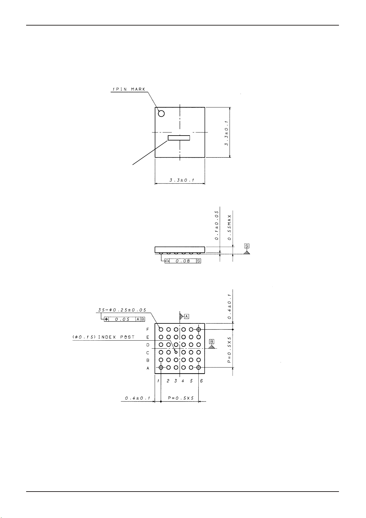
●Pin Arrangement [Bottom View]
Technical Note
F
E
D
C
B
A
T4 VBATLDO2 VBAT1 AGND VBATLDO1 T3
LDO2O LDO4O VBAT2 LDO3O LDO1O VIO
LED6 LED7 RESETB SCL SDA C1N
LED5 FLGND CPGND C2N C1P
LED4 WGND LED2 VOUT C2P VBATCP
T1 LED3 LED1 C3N C3P T2
1 2 3 4 5 6
Index
Total: 35balls
www.rohm.com
© 2011 ROHM Co., Ltd. All rights reserved.
7/28
2011.04 - Rev.
A
BD6085GUL
●Package
VCSP50L3
SIZE : 3.30mm×3.30mm
A ball pitch : 0.5mm
Height : 0.55mm max
Technical Note
BD6085
Lot No.
www.rohm.com
© 2011 ROHM Co., Ltd. All rights reserved.
8/28
2011.04 - Rev.

A
BD6085GUL
●Pin Functions
Ball
No
No.
1 B6 VBATCP - - GND Power supply for charge pump A
2 F3 VBAT1 - - GND Power supply A
3 E3 VBAT2 - - GND Power supply A
4 F5 VBATLDO1 - - GND Power supply for LDO A
5 F2 VBATLDO2 - - GND Power supply for LDO A
6 A1 T1 I VBAT GND Test Input Pin (short to Ground) S
7 A6 T2 I VBAT GND Test Input Pin (short to Ground) S
8 F6 T3 O VBAT GND Test Output Pin (Open) M
9 F1 T4 O VBAT GND Test Output Pin (Open) N
10 E6 VIO - VBAT GND Power supply for I/O and Digital C
11 D3 RESETB I VBAT GND Reset input (L: reset, H: reset cancel) H
12 D5 SDA I/O VBAT GND I2C data input / output I
13 D4 SCL I VBAT GND I2C clock input H
14 C4 CPGND - VBAT - Ground B
15 F4 AGND - VBAT - Ground B
16 B2 WGND - VBAT - Ground B
17 C2 FLGND - VBAT - Ground B
18 D6 C1N I/O VBAT GND Charge Pump capacitor is connected F
19 C6 C1P I/O - GND Charge Pump capacitor is connected G
20 C5 C2N I/O VBAT GND Charge Pump capacitor is connected F
21 B5 C2P I/O - GND Charge Pump capacitor is connected G
22 A4 C3N I/O VBAT GND Charge Pump capacitor is connected F
23 A5 C3P I/O - GND Charge Pump capacitor is connected G
24 B4 VOUT O - GND Charge Pump output pin A
25 E5 LDO1O O VBAT GND LDO1 output pin Q
26 E1 LDO2O O VBAT GND LDO2 output pin Q
27 E4 LDO3O O VBAT GND LDO3 output pin Q
28 E2 LDO4O O VBAT GND LDO4 output pin Q
29 A3 LED1 I - GND LED cathode connection 1 (for Back Light) E
30 B3 LED2 I - GND LED cathode connection 2 (for Back Light) E
31 A2 LED3 I - GND LED cathode connection 3 (for Back Light) E
32 B1 LED4 I - GND LED cathode connection 4 (for Back Light) E
33 C1 LED5 I - GND LED cathode connection 5 (for Back Light or Flash) E
34 D1 LED6 I - GND LED cathode connection 6 (for Back Light or Flash) E
35 D2 LED7 I - GND LED cathode connection 7 (for Back Light or Flash) E
※The LED terminal that isn't used is to short-circuit to the ground. But, the setup of a register concerned with LED that isn't used is prohibited.
Total: 35Pin
Pin Name I/O
ESD Diode
For
Power
For
Ground
Functions
Technical Note
Equivalent
Circuit
www.rohm.com
© 2011 ROHM Co., Ltd. All rights reserved.
9/28
2011.04 - Rev.

A
BD6085GUL
●Equivalent Circuit
A VBATB
C
VBAT
Technical Note
VBATD
E
M
VBAT VBAT
F G
VBAT
VIO VBAT I VIOVBAT
J
N
VBAT
K
O
VBAT
H
VIOVIO
P
VBAT VBAT
VIOVBAT
VBATVBAT L
Q
VBAT VBAT
www.rohm.com
© 2011 ROHM Co., Ltd. All rights reserved.
R
VBATVBAT
S VIO VBAT
VBATVBAT
10/28
T
2011.04 - Rev.
A
BD6085GUL
Technical Note
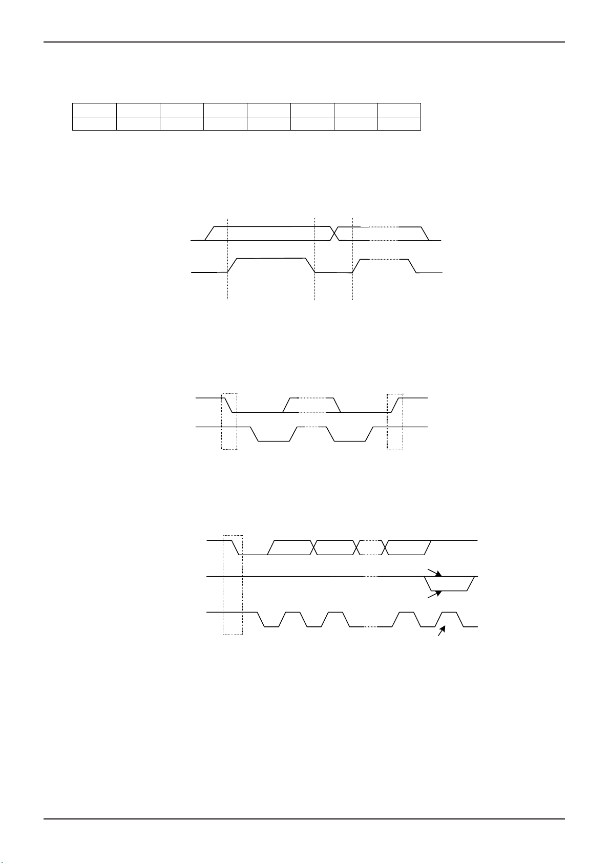
●I2C BUS format
The writing/reading operation is based on the I2C slave standard.
・Slave address
A7 A6 A5 A4 A3 A2 A1 R/W
1 1 1 0 1 1 0 1/0
・Bit Transfer
SCL transfers 1-bit data during H. SCL cannot change signal of SDA during H at the time of bit transfer. If SDA changes
while SCL is H, START conditions or STOP conditions will occur and it will be interpreted as a control signal.
SDA
SCL
SDA a state of stability
Data are effective
SDA
:
It can change
・START and STOP condition
When SDA and SCL are H, data is not transferred on the I
2
C- bus. This condition indicates, if SDA changes from H to L
while SCL has been H, it will become START (S) conditions, and an access start, if SDA changes from L to H while SCL
has been H, it will become STOP (P) conditions and an access end.
SDA
SCL
S P
START condition
STOP condition
・Acknowledge
It transfers data 8 bits each after the occurrence of START condition. A transmitter opens SDA after transfer 8bits data, and
a receiver returns the acknowledge signal by setting SDA to L.
DATA OUTPUT
BY TRANSMITTER
DATA OUTPUT
BY RECEIVER
SCL
START condition
S
12 89
not acknowledge
acknowledge
clock pulse for
acknowledgement
www.rohm.com
© 2011 ROHM Co., Ltd. All rights reserved.
11/2 8
2011.04 - Rev.

A
BD6085GUL
A A
A
A
A
A
A5A4A3A2A1A
A
A
A
A
A
A
A
A A
A
A
A6A5A4A3A2A1A
A
A
A
A
Technical Note
・Writing protocol
A register address is transferred by the next 1 byte that transferred the slave address and the write-in command. The 3rd
byte writes data in the internal register written in by the 2nd byte, and after 4th byte or, the increment of register address is
carried out automatically. However, when a register address turns into the last address, it is set to 00h by the next
transmission. After the transmission end, the increment of the address is carried out.
*1 *1
X X X X X X X
S
7
6
register addressslave address
R/W=0(write)
from master to slave
from slave to master
D7D6 D5 D4 D3 D2 D1 D0 D7 D6 D5 D4 D3 D2 D1 D0
00
DATA
register address
increment
=acknowledge(SDA LOW)
=not acknowledge(SDA HIGH)
S=START condition
P=STOP condition
*1: Write Timing
DATA
register address
・Reading protocol
It reads from the next byte after writing a slave address and R/W bit. The register to read considers as the following address
accessed at the end, and the data of the address that carried out the increment is read after it. If an address turns into the
last address, the next byte will read out 00h. After the transmission end, the increment of the address is carried out.
X X X X X X X
R/W=1(read)
from master to slave
from slave to master
P
D7 D6 D5 D4 D3 D2 D1 D0 D7 D6 D5 D4 D3 D2 D1 D0
DATA
register address
increment
=acknowledge(SDA LOW)
=not acknowledge(SDA HIGH)
S=START condition
P=STOP condition
DATA slave address
register address
increment
1 S
・Multiple reading protocols
After specifying an internal address, it reads by repeated START condition and changing the data transfer direction. The
data of the address that carried out the increment is read after it. If an address turns into the last address, the next byte will
read out 00h. After the transmission end, the increment of the address is carried out.
P
increment
S
slave address
R/W=0(write)
from master to slave
from slave to master
0
7
register address
D7 D6 D5 D4 D3D2D1D0 D7D6 D5 D4 D3 D2 D1 D0
DATA DATA
register address
increment
Sr 1
0X X X X X X X
X X X X X X X
slave address
=acknowledge(SDA LOW)
=not acknowledge(SDA HIGH)
S=START condition
P=STOP condition
Sr=repeated START condition
R/W=1(read)
P
register address
increment
As for reading protocol and multiple reading protocols, please do A(not acknowledge) after doing the final reading
operation. It stops with read when ending by A(acknowledge), and SDA stops in the state of Low when the reading
data of that time is 0. However, this state returns usually when SCL is moved, data is read, and A(not acknowledge)
is done.
www.rohm.com
© 2011 ROHM Co., Ltd. All rights reserved.
12/28
2011.04 - Rev.

A
BD6085GUL
S
●Timing diagram
SDA
CL
t
LOW
Technical Note
BUF
t
SU;DAT
t
t
HD;STA
t SU;STO
S
SU;STA
t
HD;STA
t
HD;DAT
S Sr P
t
t HIGH
●Electrical Characteristics(Unless otherwise specified, Ta=25 ℃, VBAT=3.6V, VIO=1.8V)
Standard-mode Fast-mode
Min. Typ. Max. Min. Typ. Max.
Unit
2
【I
C BUS format】
Parameter Symbol
SCL clock frequency fSCL 0 - 100 0 - 400 kHz
LOW period of the SCL clock tLOW 4.7 - - 1.3 - - μs
HIGH period of the SCL clock tHIGH 4.0 - - 0.6 - - μs
Hold time (repeated) START condition
After this period, the first clock is generated
Set-up time for a repeated START
condition
tHD;STA 4.0 - - 0.6 - - μs
SU;STA 4.7 - - 0.6 - - μs
t
Data hold time tHD;DAT 0 - 3.45 0 - 0.9 μs
Data set-up time tSU;DAT 250 - - 100 - - ns
Set-up time for STOP condition tSU;STO 4.0 - - 0.6 - - μs
Bus free time between a STOP
and START condition
BUF 4.7 - - 1.3 - - μs
t
www.rohm.com
© 2011 ROHM Co., Ltd. All rights reserved.
13/28
2011.04 - Rev.

A
BD6085GUL
●Register List
Address
00h
01h
02h
03h
04h
05h
06h
D7 D6 D5 D4 D3 D2 D1 D0
- GRPSET2 GRPSET1 GRPSET0 - - - SFTRST
- LDO4EN LDO3EN LDO2EN LDO1EN FLLEDEN SLEDEN MLEDEN Enable Control
- - - IMLED4 IMLED3 IMLED2 IMLED1 IMLED0 Main LED Current Setting
- - - ISLED4 ISLED3 ISLED2 ISLED1 ISLED0 Sub LED Current Setting
- - FLASHEN IFLLED4 IFLLED3 IFLLED2 IFLLED1 IFLLED0
LDO2VSEL3 LDO2VSEL2 LDO2VSEL1 LDO2VSEL0 LDO1VSEL3 LDO1VSEL2 LDO1VSEL1 LDO1VSEL0
LDO4VSEL3 LDO4VSEL2 LDO4VSEL1 LDO4VSEL0 LDO3VSEL3 LDO3VSEL2 LDO3VSEL1 LDO3VSEL0
Register data
Input "0” for "-".
Prohibit to accessing the address that isn’t mentioned.
●Register Map
Address 00h < Software Reset, LED Lighting group Setting >
Address R/W Bit7 Bit6 Bit5 Bit4 Bit3 Bit2 Bit1 Bit0
Technical Note
Function
Software Reset
LED Lighting group Setting
Flash LED Current Setting
Flash mode Setting
LDO1 Vout Control
LDO2 Vout Control
LDO3 Vout Control
LDO4 Vout Control
00h R/W - GRPSET2 GRPSET1 GRPSET0 - - - SFTRST
Initial
Value
00h - 0 0 0 - - - 0
Bit7 : (Not used)
Bit [6:4] : GRPSET [2:0]
(Main group) (Sub group) (Flash group)
“000” : LED1~4 --- LED5~7
“001” : LED1~4 LED5 LED6~7
“010” : LED1~4 LED5~6 LED7
“011” : LED1~4 LED5 LED7
“100” : LED1~5 LED6 LED7
“101” : LED1~5 --- LED6~7
“110” : LED1~6 --- LED7
“111” : LED1~ 6 --- LED7
Bit [3:1] : (Not used)
Bit0 : SFTRST
“0” : Reset cancel
“1” : Reset (All register initializing)
www.rohm.com
© 2011 ROHM Co., Ltd. All rights reserved.
14/28
2011.04 - Rev.

A
BD6085GUL
Address 01h < Enable Control >
Address R/W Bit7 Bit6 Bit5 Bit4 Bit3 Bit2 Bit1 Bit0
01h R/W - LDO4EN LDO3EN LDO2EN LDO1EN FLLEDEN SLEDEN MLEDEN
Initial
Value
Bit7 : (Not used)
Bit6 : LDO4EN
Bit5 : LDO3EN
Bit4 : LDO2EN
Bit3 : LDO1EN
Bit2 : FLLEDEN
Bit1 : SLEDEN
Bit0 : MLEDEN
00h - 0 0 0 0 0 0 0
“0” : LDO4 OFF
“1” : LDO4 ON
“0” : LDO3 OFF
“1” : LDO3 ON
“0” : LDO2 OFF
“1” : LDO2 ON
“0” : LDO1 OFF
“1” : LDO1 ON
“0” : Flash LED OFF
“1” : Flash LED ON
“0” : Sub LED OFF
“1” : Sub LED ON
“0” : Main LED OFF
“1” : Main LED ON
Technical Note
www.rohm.com
© 2011 ROHM Co., Ltd. All rights reserved.
15/28
2011.04 - Rev.

A
BD6085GUL
Address 02h < Main LED Current Setting >
Address R/W Bit7 Bit6 Bit5 Bit4 Bit3 Bit2 Bit1 Bit0
02h R/W - - - IMLED4 IMLED3 IMLED2 IMLED1 IMLED0
Initial
Value
Bit[7:5] : (Not used)
Bit[4:0] : IMLED [4:0]
00h - - - 0 0 0 0 0
“00000” : 0.9375 mA (Initial value)
“00001” : 1.875 mA
“00010” : 2.8125 mA
“00011” : 3.75 mA
“00100” : 4.6875 mA
“00101” : 5.625 mA
“00110” : 6.5625 mA
“00111” : 7.5 mA
“01000” : 8.4375 mA
“01001” : 9.375 mA
“01010” : 10.3125 mA
“01011” : 11.25 mA
“01100” : 12.1875 mA
“01101” : 13.125 mA
“01110” : 14.0625 mA
“01111” : 15 mA
“10000” : 15.9375 mA
“10001” : 16.875 mA
“10010” : 17.8125 mA
“10011” : 18.75 mA
“10100” : 19.6875 mA
“10101” : 20.625 mA
“10110” : 21.5625 mA
“10111” : 22.5 mA
“11000” : 23.4375 mA
“11001” : 24.375 mA
“11010” : 25.3125 mA
“11011” : 26.25 mA
“11100” : 27.1875 mA
“11101” : 28.125 mA
“11110 ” : 29.0 625 mA
“11111” : 30 m A
* LED Current : 30 x 1/32 mA Step
Technical Note
www.rohm.com
© 2011 ROHM Co., Ltd. All rights reserved.
16/28
2011.04 - Rev.

A
BD6085GUL
Address 03h < Sub LED Current Setting >
Address R/W Bit7 Bit6 Bit5 Bit4 Bit3 Bit2 Bit1 Bit0
03h R/W - - - ISLED4 ISLED3 ISLED2 ISLED1 ISLED0
Initial
Value
Bit[7:5] : (Not used)
Bit[4:0] : ISLED [4:0]
00h - - - 0 0 0 0 0
“00000” : 0.9375 mA (Initial value)
“00001” : 1.875 mA
“00010” : 2.8125 mA
“00011” : 3.75 mA
“00100” : 4.6875 mA
“00101” : 5.625 mA
“00110” : 6.5625 mA
“00111” : 7.5 mA
“01000” : 8.4375 mA
“01001” : 9.375 mA
“01010” : 10.3125 mA
“01011” : 11.25 mA
“01100” : 12.1875 mA
“01101” : 13.125 mA
“01110” : 14.0625 mA
“01111” : 15 mA
“10000” : 15.9375 mA
“10001” : 16.875 mA
“10010” : 17.8125 mA
“10011” : 18.75 mA
“10100” : 19.6875 mA
“10101” : 20.625 mA
“10110” : 21.5625 mA
“10111” : 22.5 mA
“11000” : 23.4375 mA
“11001” : 24.375 mA
“11010” : 25.3125 mA
“11011” : 26.25 mA
“11100” : 27.1875 mA
“11101” : 28.125 mA
“11110 ” : 29.0 625 mA
“11111” : 30 m A
* LED Current : 30 x 1/32 mA Step
Technical Note
www.rohm.com
© 2011 ROHM Co., Ltd. All rights reserved.
17/28
2011.04 - Rev.

A
BD6085GUL
Address 04h < Flash LED Current Setting, Flash mode Setting >
Address R/W Bit7 Bit6 Bit5 Bit4 Bit3 Bit2 Bit1 Bit0
04h R/W - - FLASHEN IFLLED4 IFLLED3 IFLLED2 IFLLED1 IFLLED0
Initial
Value
Bit[7:6] : (Not used)
Bit5 : FLASHEN
Bit[4:0] : IFLLED [4:0]
00h - - 0 0 0 0 0 0
“0” : Flash mode OFF
“1” : Flash mode ON (x4 normal mode)
(At FLASHEN=0) (At FLASHEN=1)
“00000” : 0.9375 mA, 3.75 mA (Initial value)
“00001” : 1.875 mA, 7.5 mA
“00010” : 2.8125 mA, 11.25 mA
“00011” : 3.75 mA, 15 mA
“00100” : 4.6875 mA, 18.75 mA
“00101” : 5.625 mA, 22.5 mA
“00110” : 6.5625 mA, 26.25 mA
“00111” : 7.5 mA, 30 mA
“01000” : 8.4375 mA, 33.75 mA
“01001” : 9.375 mA, 37.5 mA
“01010” : 10.3125 mA, 41.25 mA
“01011” : 11.25 mA, 45 mA
“01100” : 12.1875 mA, 48.75 mA
“01101” : 13.125 mA, 52.5 mA
“01110” : 14.0625 mA, 56.25 mA
“01111” : 15 mA, 60 mA
“10000” : 15.9375 mA, 63.75 mA
“10001” : 16.875 mA, 67.5 mA
“10010” : 17.8125 mA, 71.25 mA
“10011” : 18.75 mA, 75 mA
“10100” : 19.6875 mA, 78.75 mA
“10101” : 20.625 mA, 82.5 mA
“10110” : 21.5625 mA, 86.25 mA
“10111” : 22.5 mA, 90 mA
“11000” : 23.4375 mA, 93.75 mA
“11001” : 24.375 mA, 97.5 mA
“11010” : 25.3125 mA, 101.25 mA
“11011” : 26.25 mA, 105 mA
“11100” : 27.1875 mA. 108.75 mA
“11101” : 28.125 mA, 112.5 mA
“11110 ” : 29.0 625 mA, 116.25 mA
“11111” : 30 m A , 120 mA
* LED Current : 30 x 1/32 mA Step (at FLASHEN=0), 120 x 1/32 mA Step (at FLASHEN=1)
Technical Note
www.rohm.com
© 2011 ROHM Co., Ltd. All rights reserved.
18/28
2011.04 - Rev.

A
BD6085GUL
Address 05h < LDO1 Vout Control, LDO2 Vout Control >
Address R/W Bit7 Bit6 Bit5 Bit4 Bit3 Bit2 Bit1 Bit0
Technical Note
05h R/W
Initial
Value
Bit[7:4] : LDO2VSEL [3:0]
Bit[3:0] : LDO1VSEL [3:0]
74h 0 1 1 1 0 1 0 0
LDO2VSEL3 LDO2VSEL2 LDO2VSEL1 LDO2VSEL0 LDO1VSEL3 LDO1VSEL2 LDO1VSEL1 LDO1VSEL0
“0000” : 1.20 V
“0001” : 1.30 V
“0010” : 1.50 V
“0011” : 1.60 V
“0100” : 1.80 V
“0101” : 2.20 V
“0110” : 2.40 V
“0111” : 2.50 V (Initial value)
“1000” : 2.60 V
“1001” : 2.70 V
“1010” : 2.80 V
“1011” : 2.90 V
“1100” : 3.00 V
“1101” : 3.10 V
“1110” : 3.20 V
“1111” : 3. 30 V
“0000” : 1.20 V
“0001” : 1.30 V
“0010” : 1.50 V
“0011” : 1.60 V
“0100” : 1.80 V (Initial value)
“0101” : 2.20 V
“0110” : 2.40 V
“0111” : 2.50 V
“1000” : 2.60 V
“1001” : 2.70 V
“1010” : 2.80 V
“1011” : 2.90 V
“1100” : 3.00 V
“1101” : 3.10 V
“1110” : 3.20 V
“1111” : 3. 30 V
www.rohm.com
© 2011 ROHM Co., Ltd. All rights reserved.
19/28
2011.04 - Rev.

A
BD6085GUL
Address 06h < LDO3 Vout Control, LDO4 Vout Control >
Address R/W Bit7 Bit6 Bit5 Bit4 Bit3 Bit2 Bit1 Bit0
Technical Note
06h R/W
Initial
Value
Bit[7:4] : LDO4VSEL [3:0]
Bit[3:0] : LDO3VSEL [3:0]
A4h 1 0 1 0 0 1 0 0
LDO4VSEL3 LDO4VSEL2 LDO4VSEL1 LDO4VSEL0 LDO3VSEL3 LDO3VSEL2 LDO3VSEL1 LDO3VSEL0
“0000” : 1.20 V
“0001” : 1.30 V
“0010” : 1.50 V
“0011” : 1.60 V
“0100” : 1.80 V
“0101” : 2.20 V
“0110” : 2.40 V
“0111” : 2.50 V
“1000” : 2.60 V
“1001” : 2.70 V
“1010” : 2.80 V (Initial value)
“1011” : 2.90 V
“1100” : 3.00 V
“1101” : 3.10 V
“1110” : 3.20 V
“1111” : 3. 30 V
“0000” : 1.20 V
“0001” : 1.30 V
“0010” : 1.50 V
“0011” : 1.60 V
“0100” : 1.80 V (Initial value)
“0101” : 2.20 V
“0110” : 2.40 V
“0111” : 2.50 V
“1000” : 2.60 V
“1001” : 2.70 V
“1010” : 2.80 V
“1011” : 2.90 V
“1100” : 3.00 V
“1101” : 3.10 V
“1110” : 3.20 V
“1111” : 3. 30 V
www.rohm.com
© 2011 ROHM Co., Ltd. All rights reserved.
20/28
2011.04 - Rev.

A
BD6085GUL
V
V
Technical Note
●Explanation for operate
1. Reset
There are two kinds of reset, software reset and hardware reset.
(1) Software reset
・All the registers are initialized more than making a register (SFTRST) setup "1".
・The register of software resetting is an automatic return (Auto Return 0).
(2) Hardware reset
・It shifts to hardware reset by changing RESETB pin “H” → “L”.
・The condition of all the registers under hardware reset pin is returned to the initial value,
and it stops accepting all address.
・It’s possible to release from a state of hardware reset by changing RESETB pin “L” → “H”.
・RESETB pin has delay circuit. It doesn’t recognize as hardware reset in “L” period under 5μs.
(3) Reset Sequence
・When hardware reset was done during software reset, software reset is canceled when
hardware reset is canceled. (Because the initial value of software reset is “0”)
2. Thermal shutdown
The blocks which thermal shutdown function is effective in the following.
Charge pump
LED Driver
LDO1, LDO2, LDO3, LDO4
A thermal shutdown function works in about 190
Detection temperature has a hysteresis, and detection release temperature is about 170
℃.
℃.
(Design reference value)
3. Charge Pump for LED driver
Charge Pump block is designed for the power supply for LED driver.
It has the x1.0/x1.33/x1.5/x2.0 mode. it changes to the most suitable mode automatically by Vf of LED and the battery
voltage. It has the mode of x1.33 and it can be higher efficiency than traditional.
Start
Charge Pump circuit operates when any LED turns ON.
Soft start
When the start of the Charge Pump circuit is done, it has the soft start function to prevent a rush current.
BAT
T
IO
RESETB
EN (*1)
VBATON
T
VIOON=min 0.1ms
T
RSTB=min 0.1ms
T
SOFT
T
VBATOFF
T
VIOOFF=min 1ms
T
RST=min 0ms
VOUT
LED Current
www.rohm.com
© 2011 ROHM Co., Ltd. All rights reserved.
(*1) An EN signal in the upper figure means the following;
“EN is high” = Any LED turns ON
But if Ta >TSD, EN Signal doesn’t become effective.
21/28
2011.04 - Rev.

A
BD6085GUL
Charge Pump Mode transition
The transition of boost multiple transits automatically by Vf of LED and the battery voltage.
BD6085GUL changes the four charge pump movement mode automatically to realize low consumption power.
< Mode Up >
A LED terminal voltage is monitored, and the movement mode is changed to ×1→×1.33, ×1.33→×1.5 and ×1.5→×2
automatically when a LED terminal voltage is lower than 0.2V (typ).
At this time, the maximum output voltage of the charge pump is restricted to 5.1V (typ).
< Mode Down >
The rise in the battery voltage, the off control of LED lighting and the data writing to the address 02h,03h,04h (LED
Current Setting) is monitored, and the movement mode is changed to ×2→×1.5→×1.33→×1 automatically at FLASHEN
(Address 04h) =“0”. This mode down movement lasts until a mode up movement happens. At FLASHEN=“1”, the mode
down doesn't happen.
The thresholds of rise in a battery voltage are 2.9V, 3.3V, 3.7V and 4.1V (typ).
And, as for the off control of LED lighting, it is shown that MLEDEN, SLEDEN and FLLEDEN (Address 01h) and
FLASHEN (Address 04h) transited in “1”→“0”.
Over Voltage protection / Over Current protection
Charge Pump circuit output (VOUT) is equipped with the over-voltage protection and the over current protection function.
A VOUT over-voltage detection voltage is about 5.5V(typ). (VOUT at the time of rise in a voltage)
A detection voltage has a hysteresis, and a detection release voltage is about 5.1V(typ).
And, when VOUT output short to ground, input current of the battery terminal is limited by an over current protection
function.
All LED OFF
RESET
mode down=”H”
mode down=”H”
mode down=”H”
STANDBY
1
○
SOFT
After “VOUT>1.5V(typ)” detected, 142us(typ) wait
X1.0
X1.33
X1.5
X2.0
ALL off
Any LED on
Ta< T
TSD
VBAT>2.3V(typ)
CP x1.0 mode
CP x1.0 mode
mode up=”H”
CP x1.33 mode
mode up=”H”
CP x1.5mode
mode up=”H”
CP x2.0mode
Technical Note
www.rohm.com
© 2011 ROHM Co., Ltd. All rights reserved.
22/28
2011.04 - Rev.

A
BD6085GUL
4. LED Driver
LED current value setting (for Main/Sub)
Internal circuit fixes maximum current value of LED.
LED current is maximum 30mA/ch.
LED current value setting (for Flash)
Internal circuit fixes maximum current value of LED.
When FLASHEN (Address 04h)=0, LED current is maximum 30mA/ch. (Normal mode)
When FLASHEN (Address 04h)=1, LED current change to x4 of Normal mode. (Flash mode)
At Normal mode, it can use for LCD Backlight or Torch mode of Flash.
At Flash mode, it can use for LED Flash.
The number of LED Lighting
The number of lighting for Main/Sub/Flash LED can be set up grouping by the register GRPSET*
(Address 00h).
The setting of the number of lighting is as the following.
The grouping of LED (Main/Sub/Flash) is independently controlled by register MLEDEN, SLEDEN, FLLEDEN
(Address 01h).
Grouping
setting
(0,0,0) Main Main Main Main Flash Flash Flash 4 / 0 / 3
(0,0,1) Main Main Main Main Sub Flash Flash 4 / 1 / 2
(0,1,0) Main Main Main Main Sub Sub Flash 4 / 2 / 1
(0,1,1) Main Main Main Main Sub - Flash 4 / 1 / 1
(1,0,0) Main Main Main Main Main Sub Flash 5 / 1 / 1
(1,0,1) Main Main Main Main Main Flash Flash 5 / 0 / 2
(1,1,0) Main Main Main Main Main Main Flash 6 / 0 / 1
(1,1,1) Main Main Main Main Main Main Flash 6 / 0 / 1
The change of the Grouping setting with turning it on is prohibited.
The LED terminal that isn’t used must be connected to the ground.
Normal mode/Flash mode
Normal mode and Flash mode change as the figure of the follow.
ILED is set by the register.
LED1 LED2 LED3 LED4 LED5 LED6 LED7 Main/Sub/Flash
Grouping setting (*,*,*) means (“GRPSET2”,”GRPSET1”,”GRPSET0”).
FLLEDEN
Technical Note
FLASHEN
LED current
www.rohm.com
© 2011 ROHM Co., Ltd. All rights reserved.
ILED
Normal mode
4×ILED
Flash mode
23/28
Normal mode
2011.04 - Rev.

A
BD6085GUL
V
V
5. I/O
When the RESETB pin is Low, the input buffers (SDA and SCL) are disable for the Low consumption power.
Technical Note
VBAT
VIO
EN
RESETB=L, Output “H”
LOGIC
Level
Shift
SCL
(SDA)
RESETB
6. About the start of LDO1~LDO4
It must start as follows.
BAT
IO
RESETB
LDO1EN or LDO2EN or
LDO3EN or LDO4EN
LDO1O or LDO2O or
LDO3O or LDO4O
(LDO output)
T
VBATON
T
VIOON=min 0.1ms
T
RSTB=min 0.1ms
T
RISE = max 1ms
T
VBATOFF
T
VIOOFF=min 1ms
T
RST=min 0ms
<Start Sequence>
VBAT ON (Enough rise up) → VIO ON (Enough rise up) → Reset release → LDO ON
(Register access acceptable)
<End Sequence>
LDO OFF → Reset → VIO OFF (Enough fall down) → VBAT OFF
7. About the terminal management of the function that isn't used
Set up the terminal that isn't used as follows.
The LED terminal which isn't used : Short to ground
Don't do the control concerned with this terminal.
T1, T2 : Short to ground
T3, T4 : Open
www.rohm.com
© 2011 ROHM Co., Ltd. All rights reserved.
24/28
2011.04 - Rev.

A
BD6085GUL
●PCB pattern of the Power dissipation measuring board
1st layer(component) 2nd layer
Technical Note
3
5
rd
layer 4th layer
th
layer 6th layer
7th layer 8th layer(solder)
www.rohm.com
© 2011 ROHM Co., Ltd. All rights reserved.
25/28
2011.04 - Rev.

A
BD6085GUL
●Cautions on use
(1) Absolute Maximum Ratings
An excess in the absolute maximum ratings, such as supply voltage, temperature range of operating conditions, etc.,
can break down devices, thus making impossible to identify breaking mode such as a short circuit or an open circuit. If
any special mode exceeding the absolute maximum ratings is assumed, consideration should be given to take physical
safety measures including the use of fuses, etc.
(2) Power supply and ground line
Design PCB pattern to provide low impedance for the wiring between the power supply and the ground lines. Pay
attention to the interference by common impedance of layout pattern when there are plural power supplies and ground
lines. Especially, when there are ground pattern for small signal and ground pattern for large current included the
external circuits, please separate each ground pattern. Furthermore, for all power supply pins to ICs, mount a capacitor
between the power supply and the ground pin. At the same time, in order to use a capacitor, thoroughly check to be sure
the characteristics of the capacitor to be used present no problem including the occurrence of capacity dropout at a low
temperature, thus determining the constant.
(3) Ground voltage
Make setting of the potential of the ground pin so that it will be maintained at the minimum in any operating state.
Furthermore, check to be sure no pins are at a potential lower than the ground voltage including an actual electric
transient.
(4) Short circuit between pins and erroneous mounting
In order to mount ICs on a set PCB, pay thorough attention to the direction and offset of the ICs. Erroneous mounting
can break down the ICs. Furthermore, if a short circuit occurs due to foreign matters entering between pins or between
the pin and the power supply or the ground pin, the ICs can break down.
Technical Note
(5) Operation in strong electromagnetic field
Be noted that using ICs in the strong electromagnetic field can malfunction them.
(6) Input pins
In terms of the construction of IC, parasitic elements are inevitably formed in relation to potential. The operation of the
parasitic element can cause interference with circuit operation, thus resulting in a malfunction and then breakdown of
the input pin. Therefore, pay thorough attention not to handle the input pins, such as to apply to the input pins a voltage
lower than the ground respectively, so that any parasitic element will operate. Furthermore, do not apply a voltage to the
input pins when no power supply voltage is applied to the IC. In addition, even if the power supply voltage is applied,
apply to the input pins a voltage lower than the power supply voltage or within the guaranteed value of electrical
characteristics.
(7) External capacitor
In order to use a ceramic capacitor as the external capacitor, determine the constant with consideration given to a
degradation in the nominal capacitance due to DC bias and changes in the capacitance due to temperature, etc.
(8) Thermal shutdown circuit (TSD)
This LSI builds in a thermal shutdown (TSD)circuit. When junction temperatures become detection temperature or
higher, the thermal shutdown circuit operates and turns a switch OFF. The thermal shutdown circuit, which is aimed at
isolating the LSI from thermal runaway as much as possible, is not aimed at the protection or guarantee of the LSI.
Therefore, do not continuously use the LSI with this circuit operating or use the LSI assuming its operation.
(9) Thermal design
Perform thermal design in which there are adequate margins by taking into account the permissible dissipation (Pd)in
actual states of use.
(10) LDO
Use each output of LDO by the independence. Don’t use under the condition that each output is short-circuited because
it has the possibility that an operation becomes unstable.
(11) About the pin for the test, the un-use pin
Prevent a problem from being in the pin for the test and the un-use pin under the state of actual use. Please refer to a
function manual and an application notebook. And, as for the pin that doesn't specially have an explanation, ask our
company person in charge.
(12) About the rush current
For ICs with more than one power supply, it is possible that rush current may flow instantaneously due to the internal
powering sequence and delays. Therefore, give special consideration to power coupling capacitance, power wiring,
width of ground wiring, and routing of wiring.
(13) About the function description or application note or more.
The function description and the application notebook are the design materials to design a set. So, the contents of the
materials aren't always guaranteed. Please design application by having fully examination and evaluation include the
external elements.
www.rohm.com
© 2011 ROHM Co., Ltd. All rights reserved.
26/28
2011.04 - Rev.
A
BD6085GUL
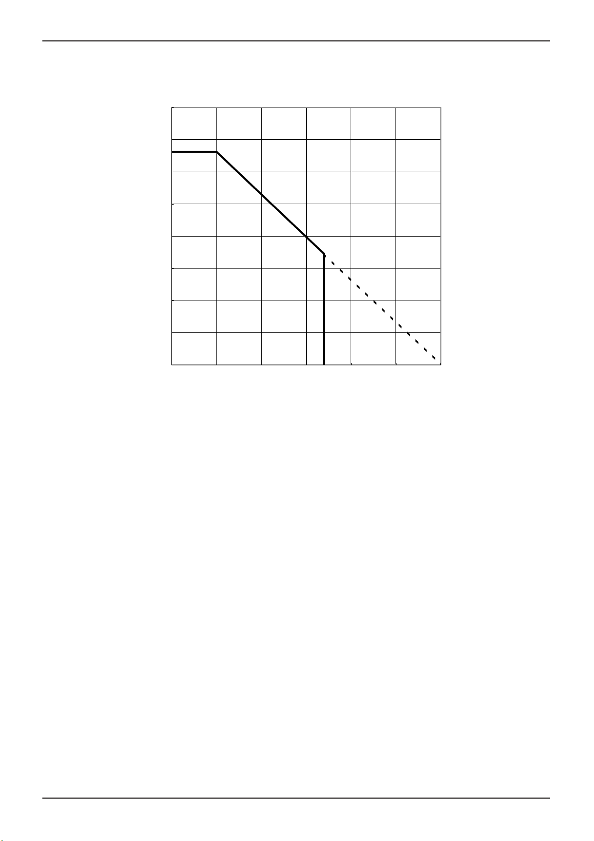
●Power dissipation (On the ROHM’s standard board)
1.6
1.4
1325mW
1.2
1.0
0.8
Power Dissipation Pd (W)
0.6
0.4
Technical Note
0.2
0.0
0 25 50 75 100 125 150
Ta(℃)
Information of the ROHM’s standard board
Material : glass-epoxy
Size : Refer to after page.
www.rohm.com
© 2011 ROHM Co., Ltd. All rights reserved.
27/28
2011.04 - Rev.

A
BD6085GUL
●Ordering part number
Technical Note
B D
Part No. Part No.
VCSP50L3
(BD6085GUL)
1PIN MARK
35-φ0.25±0.05
0.05
(φ0.15)INDEX POST
0.4±0.1
BA
F
E
D
C
B
A
6 0 8 5
6085
3.3±0.1
3.3±0.1
0.08 S
A
123456
P=0.5× 5
0.1±0.05
0.55MAX
S
0.4±0.1
B
P=0.5× 5
(Unit : mm)
GU L
Package
GUL : VCSP50L3
<Tape and Reel information>
Embossed carrier tapeTape
Quantity
Direction
of feed
2500pcs
E2
The direction is the 1pin of product is at the upper left when you hold
()
reel on the left hand and you pull out the tape on the right hand
Reel
-
E 2
Packaging and forming specification
E2: Embossed tape and reel
1pin
Order quantity needs to be multiple of the minimum quantity.
∗
Direction of feed
www.rohm.com
© 2011 ROHM Co., Ltd. All rights reserved.
28/28
2011.04 - Rev.

Notes
No copying or reproduction of this document, in part or in whole, is permitted without the
consent of ROHM Co.,Ltd.
The content specied herein is subject to change for improvement without notice.
The content specied herein is for the purpose of introducing ROHM's products (hereinafter
"Products"). If you wish to use any such Product, please be sure to refer to the specications,
which can be obtained from ROHM upon request.
Examples of application circuits, circuit constants and any other information contained herein
illustrate the standard usage and operations of the Products. The peripheral conditions must
be taken into account when designing circuits for mass production.
Great care was taken in ensuring the accuracy of the information specied in this document.
However, should you incur any damage arising from any inaccuracy or misprint of such
information, ROHM shall bear no responsibility for such damage.
The technical information specied herein is intended only to show the typical functions of and
examples of application circuits for the Products. ROHM does not grant you, explicitly or
implicitly, any license to use or exercise intellectual property or other rights held by ROHM and
other parties. ROHM shall bear no responsibility whatsoever for any dispute arising from the
use of such technical information.
The Products specied in this document are intended to be used with general-use electronic
equipment or devices (such as audio visual equipment, ofce-automation equipment, communication devices, electronic appliances and amusement devices).
The Products specied in this document are not designed to be radiation tolerant.
While ROHM always makes efforts to enhance the quality and reliability of its Products, a
Product may fail or malfunction for a variety of reasons.
Please be sure to implement in your equipment using the Products safety measures to guard
against the possibility of physical injury, re or any other damage caused in the event of the
failure of any Product, such as derating, redundancy, re control and fail-safe designs. ROHM
shall bear no responsibility whatsoever for your use of any Product outside of the prescribed
scope or not in accordance with the instruction manual.
The Products are not designed or manufactured to be used with any equipment, device or
system which requires an extremely high level of reliability the failure or malfunction of which
may result in a direct threat to human life or create a risk of human injury (such as a medical
instrument, transportation equipment, aerospace machinery, nuclear-reactor controller, fuelcontroller or other safety device). ROHM shall bear no responsibility in any way for use of any
of the Products for the above special purposes. If a Product is intended to be used for any
such special purpose, please contact a ROHM sales representative before purchasing.
If you intend to export or ship overseas any Product or technology specied herein that may
be controlled under the Foreign Exchange and the Foreign Trade Law, you will be required to
obtain a license or permit under the Law.
Notice
www.rohm.com
© 2011 ROHM Co., Ltd. All rights reserved.
Thank you for your accessing to ROHM product informations.
More detail product informations and catalogs are available, please contact us.
ROHM Customer Support System
http://www.rohm.com/contact/
R1120
A
 Loading...