

A
LED Drivers for LCD Backlights
Multifunction Backlight LED Drivers
for Small LCD Panels (Charge Pump Type)
BD6081GU, BD6081GVW
●Description
BD6081GU / BD6081GVW is compound LED Driver which is the most suitable for the cellular phone.
Main LCD Back Light LED Driver (Max 4 Light), Sub LCD Back Light LED Driver (Max 2 Light), 2 system RGB LED Drivers,
2Ch LDO (2.8V/1.8V) included. This is PMIC (Power Management IC) that is the most suitable for "the indication part" of the
cellular phone.A charge pump form is adopted, and a coil is never used for the part DC/DC. This IC achieves compact size
with the chip size package (VCSP85H3). [BD6081GU] This IC solves a mounting problem by BGA package
(SBGA063W060). [BD6081GVW]
●Features
1) Main LCD Back Light LED Driver (Max 4 Light)
4 Lighting / 3 Lighting can be chosen (register setting)
2) Sub LCD Back Light LED Driver (Max 2 Light)
2 Lighting / 1 Lighting can be chosen (register setting)
3) RGB LED Driver (2 System)
Slope control is built in.(2 system independence can be controlled.)
LED connection (for G1LED,G2LED,B1LED,B2LED) can be set up in the battery or the DC/DC output.(register setting)
LED connection (for R1LED,R2LED) can be set up in the battery only.
4) 2ch Series Regulator
2.8V output Iomax=150mA
1.8V output Iomax=150mA(normal mode)
1.8V output low current consumption mode / normal mode Switching is possible. (The outside pin control / regi ster setting)
5) Charge Pump DC/DC
Soft start Functions
Over voltage protection (Auto-return type)
Over current protection (Auto-return type)
6) Thermal shutdown (Auto-return type)
2
7) I
●Absolute Maximum Ratings (Ta=25
C BUS Fast-mode (max 400kHz)Writing
*This chip is not designed to protect itself against radioactive rays.
*This material may be changed on its way to designing.
*This material is not the specification.
℃)
Parameter
Symbol Ratings Unit
No.11040EAT27
Maximum Applied voltage VMAX 7 V
Power Dissipation
Operating Temperature Range Topr -25 ~ +85 ℃
Storage Temperature Range Tstg -55 ~ +150 ℃
cote1)Power dissipation deleting is 13.8mW/ ℃, when it’s used in over 25 ℃.
(It’s deleting is on the board that is ROHM’s standard))
Note2)Power dissipation deleting is 8.48mW/
(It’s deleting is on the board that is ROHM’s standard))
●Operating conditions (VBATVIO, Ta=-25~85
Parameter Symbol
VBAT input voltage VBAT 2.7 ~ 5.5 V
VIO pin voltage VIO 1.65 ~ 3.3 V
www.rohm.com
© 2011 ROHM Co., Ltd. All rights reserved.
BD6081GU Pd 1725 note1) mW
BD6081GVW Pd 1060 note2) mW
℃, when it’s used in over 25 ℃.
℃)
1/35
Ratings
Unit
2011.04 - Rev.
A
BD6081GU,BD6081GVW
●Electrical Characteristics (Unless otherwise specified, Ta=25℃, VBAT=3.6V, VIO=1.8V)
Parameter Symbol
【Circuit Current】
VBAT Circuit current 1 IBAT1 - 0.1 3.0 A
VBAT Circuit current 2 IBAT2 - 0.5 3.0 A
VBAT Circuit current 3 IBAT3 - 6.2 9.5 A
VBAT Circuit current 4 IBAT4 - 100 150 A
VBAT Circuit current 5 IBAT5 - 140 210 A
VBAT Circuit current 6 IBAT6 - 63 95 mA
VBAT Circuit current 7 IBAT7 - 95 143 mA
VBAT Circuit current 8 IBAT8 - 125 188 mA
【LED Driver】
LED current Step1 ILEDSTP1 32 Step
LED current Step2 ILEDSTP2 64 Step
LED Maximum setup current 1
LED Maximum setup current 2
LED current accurate ILED 18 20 22 mA
LED current Matching ILEDMT - 5 10 %
LED OFF Leak current ILKLED - - 1.0 A
【DC/DC(Charge Pump)】
Output voltage V℃P Vf+0.15 Vf+0.2 - V
Current Load IOUT - - 255 mA
Oscillator frequency fosc 0.8 1.0 1.2 MHz
Over voltage protection
detect voltage
Over current protection
detect current
【REG1】
Output voltage Vo1 2.716 2.80 2.884 V
I/O voltage difference Vsat1 - 0.2 0.3 V
Load stability Vo11 - 10 60 mV
Input stability Vo12 - 10 60 mV
Ripple Rejection Ratio RR1 30 40 - dB
Short circuit current limit Ilim01 - 225 450 mA
Discharge resister at OFF ROFF1 - 1.0 1.5 k
【REG2】
Output voltage 1 Vo21 1.74 1.8 1.86 V
Output voltage 2 Vo22 1.71 1.8 1.89 V
Load stability Vo21 - 10 60 mV
Input stability Vo22 - 10 60 mV
Ripple Rejection Ratio RR2 30 40 - dB
Short circuit current limit Ilim02 - 225 450 mA
Discharge resister at OFF ROFF2 - 1.0 1.5 k
IMAX1 - - 32 mA
IMAX2 - - 31.5 mA
OVP - 6.0 6.5 V
OCP - 250 375 mA
Min. Typ. Max.
Limits
Unit Condition
RESET=0V, VIO=0V
RESET=0V, VIO=1.8V
REG2 low current consumption mode,
Io=0mA
REG2 normal mode, Io=0mA
REG1, REG2 normal mode, Io=0mA
DC/DC x1mode, Io=60mA,VBAT=4.0V
DC/DC x1.5mode,
Io=60mA,VBAT=3.6V
DC/DC x2 mode,
Io=60mA,VBAT=2.7V
MLED1~4, SLED1~2
R1LED, G1LED, B1LED,R2LED,
G2LED, B2LED (with 0mA setting)
MLED1~4, SLED1~2, ISET=120k
R1LED, G1LED, B1LED,R2LED,
G2LED, B2LED, ISET=120k
ILED=20mA, ISET=120k
Between MLED1~4
Between SLED1~2
Between R1LED, G1LED and B1LED
Between R2LED, G2LED and B2LED
Vf is LED forward voltage
VBAT3.2V, VOUT=4V
VOUT=0V
Io=150mA, VBAT3.1V
VBAT=2.5V, Io=150mA
Io=1~150mA
VBAT=3.2~5.5V, Io=150mA
f=100Hz, Vin=200mVp-p
Vo=0V
Io=150mA
(normal mode)
Io=100A
(low current consumption mode)
Io=1~150mA
VBAT=3.2~5.5V, Io=150mA
f=100Hz, Vin=200mVp-p
Vo=0V
Technical Note
www.rohm.com
© 2011 ROHM Co., Ltd. All rights reserved.
2/35
2011.04 - Rev.
A
BD6081GU,BD6081GVW
Technical Note
●Electrical Characteristics (Unless otherwise specified, Ta=25℃, VBAT=3.6V, VIO=1.8V)
Parameter Symbol
Min. Typ. Max.
Limits
Unit Condition
【I2C Input (SDA, SCL)】
LOW level input voltage
HIGH level input voltage
Hysteresis of Schmitt trigger input
LOW level output voltage
(SDA) at 3mA sink current
Input current each I/O pin
VIL -0.3 - 0.25 ×VIO V
VIH 0.75 ×VIO - VBAT+0.3 V
Vhys 0.05 ×VIO - - V
VOL 0 - 0.3 V
lin -10 - 10 A
Input voltage =
0.1×VIO~0.9×VIO
【RESET, RGB1CNT, RGB2CNT】
LOW level input voltage
HIGH level input voltage1
HIGH level input voltage2
Input current each I/O pin1
Input current each I/O pin2
VIL -0.3 - 0.25 ×VIO V
VIH1 0.75 ×VIO - VBAT+0.3 V
VIH2 0.75 ×VIO - VIO+0.3 V
Iin -10 - 10 A
Iin - 6 15 A
RESET Pin
RGB1CNT, RGB2CNT Pin
Input voltage =
0.1×VIO~0.9×VIO,RESET Pin
Input voltage = .9×VIO
,RGB1CNT, RGB2CNT Pin
【REG2EN, REG2MD】
LOW level input voltage
HIGH level input voltage
Input current each I/O pin
VIL -0.3 - 0.3 V
VIH 1.4 - VBAT,+0.3 V
Iin - 6 15 A Vin=1.8V
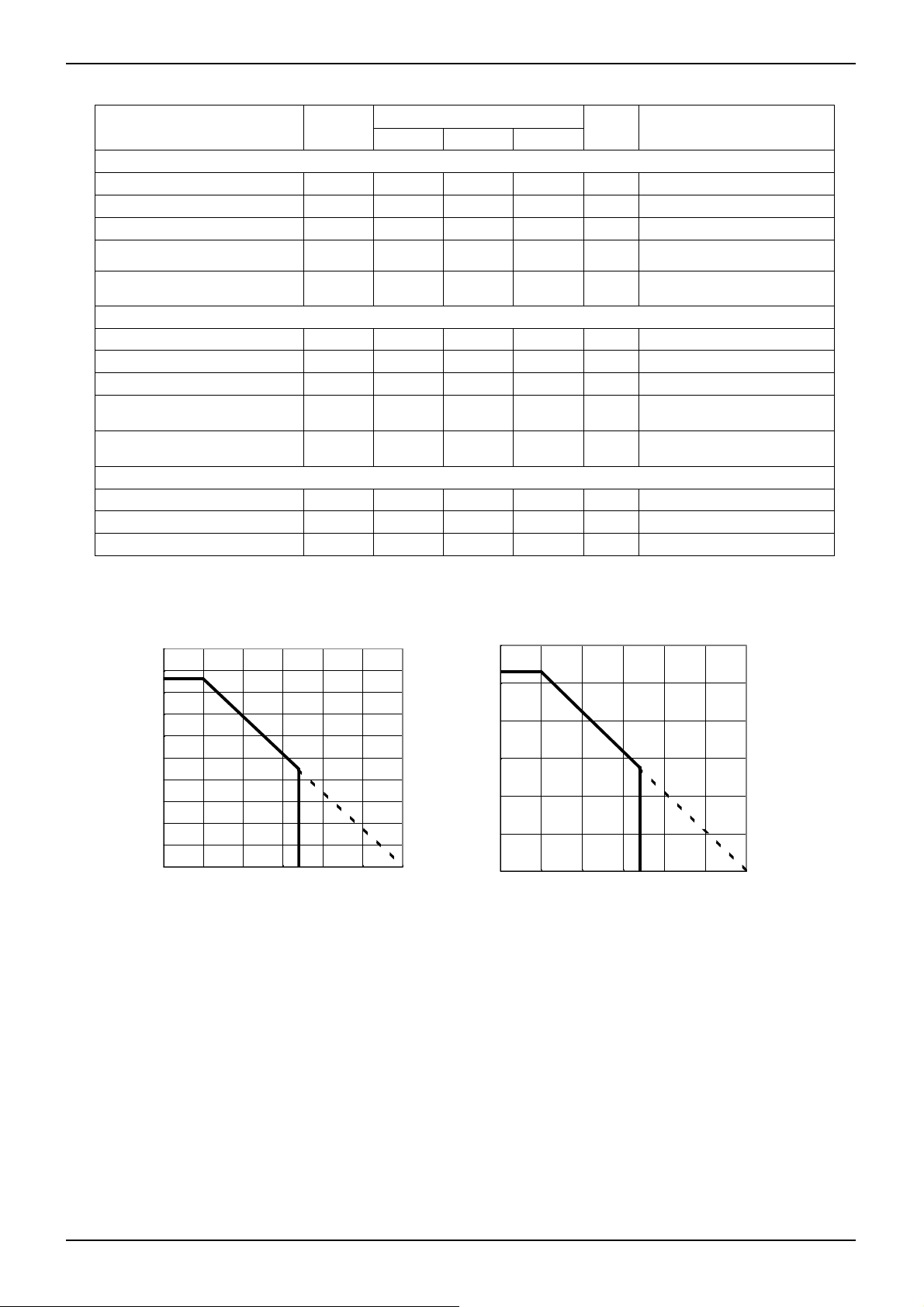
●Power dissipation (On the ROHM’s standard board)
BD6081GU BD6081GVW
2.0
1.8
1725mW
1.6
1.4
W)
1.2
(
1.0
0.8
Power Dissipation
0.6
0.4
0.2
0.0
0 25 50 75 100 125 150
Ta(
℃)
1.2
1.0
1060mW
0.8
W)
(
0.6
Power Dissipation
0.4
0.2
0.0
0 25 50 75 100 125 150
Ta( ℃)
Fig.1 Fig.2
Information of the ROHM’s standard board Information of the ROHM’s standard board
Material: glass-epoxy Material: glass-epoxy
Size: 50mm×58mm×1.75mm (8 Layer) Size: 114.3mm×76.2mm×1.6mm
Pattern of the board: Refer to it that goes later.
www.rohm.com
© 2011 ROHM Co., Ltd. All rights reserved.
3/35
2011.04 - Rev.
A
BD6081GU,BD6081GVW
A
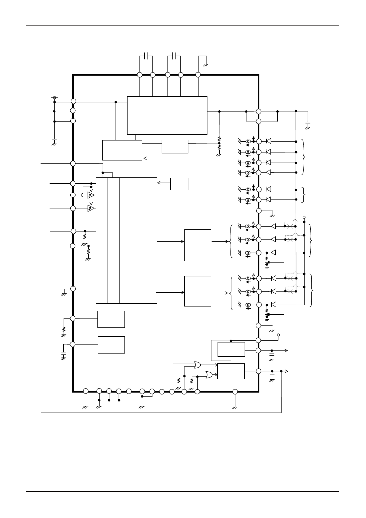
●Block Diagram / Application Circuit example
VBATCP
VBAT1
VBAT2
Charge Pump
Mode Control
VIO
RESET
SCL
SD
RGB1CNT
RGB2CNT
I/O
LEVEL
SHIFT
I2C
CONTROL
DGND
120k
0.1µF
ISET
CREF
IREF
VREF
T3
T1
REFGND
T2
T4
Fig.3 Block Diagram / Application Circuit example
1F (10V)
C1N
1F (10V)
C1P
C2N
Charge Pump
x1 / x1.5 / x2
OVP
LED terminal voltage feedback
Register control
TESTI2
TESTI1
TESTO1
TESTO2
C2P
TSD
Register control
REG2EN
CPGND
Slope
Control
(RGB1)
Slope
Control
(RGB2)
REG2MD
REG1
2.8V
Io=150mA
REG2
1.8V
Io=150mA
REGGND
VOUT
VOUTM
MLED1~4
SLED1~2
BLGND
G1LED
B1LED
R1LED
G2LED
B2LED
R2LED
RGBGND
VBATREG
REG1O
REG2O
Technical Note
VBAT
External Control
External Control
VBAT
1F
1F
1F
(10V)
Main LCD
Back Light
Sub LCD
Back Light
RGB1 LED
RGB2 LED
www.rohm.com
© 2011 ROHM Co., Ltd. All rights reserved.
4/35
2011.04 - Rev.
A
BD6081GU,BD6081GVW
●Pin Arrangement [Bottom View]
BD6081GU
T4 VBAT1 REG2O
G
REFGND R1LED CREF REG1O REG2M D
F
G1LED B1LED ISET REG2EN
E
RGBGND R2LED TESTI1 TESTI2 SCL VOUTM VOUT
D
G2LED B2LED
C
SLED1 BLGND MLED2 MLED4 CPGND C1N VBATCP
B
T1 SLED2 MLED1 MLED3 V BA T2 C2N T2
A
1234567
Total: 48ball
There is no Ball only in C3 for index.
BD6081GVW
H
T2 C1P C2P - - SDA RESET T3
G
C1N - - VOUT M TESTO 1 SCL
CPGND C2N TESTI1 VOUT DGND
F
MLED3 MLED4 VBAT2
E
MLED2 - MLED1 - - REG1O
D
(index) BLGND B2LED - - TESTI2 CR EF REG2O
C
SLE D2 SLED1 R2LED - -
B
A
T1 G2LED
12345678
Total: 63ball
There is no Ball only in C1 for index.
“-“ means NC pin (Non connect to internal circuit)
VBATREG
TESTO2 TESTO1 C1P C2P
index
RGBGND
REGGND VIO T3
RGB2CNT
VBATCP
B1LED G1LED R1LED ISET T4
-
RGB1CNT
SDA DGN D
RGB1CNT
REG2EN
REFGND
RESET
RGB2CNT
TESTO2
REGGND
VBATREG
VIO
REG2MD
-VBAT1
Technical Note
-
-
www.rohm.com
© 2011 ROHM Co., Ltd. All rights reserved.
5/35
2011.04 - Rev.
A
BD6081GU,BD6081GVW
●Package
BD6081GU
VCSP85H3 CSP small Package
SIZE : 3.90mm×3.90mm(A difference in public: X and Y, together, ± 0.1mm) height 1.0mm max
A ball pitch : 0.5mm
BD6081
Lot No.
Technical Note
www.rohm.com
© 2011 ROHM Co., Ltd. All rights reserved.
6/35
2011.04 - Rev.
A
BD6081GU,BD6081GVW
●Package
BD6081GVW
SBGA063W060
SIZE : 6.0mm×6.0mm(A difference in public: X and Y, together, ± 0.1mm) height 0.9mm max
A ball pitch : 0.65mm
BD6081
Lot No.
Technical Note
www.rohm.com
© 2011 ROHM Co., Ltd. All rights reserved.
7/35
2011.04 - Rev.

A
BD6081GU,BD6081GVW
m
Technical Note
●Pin Functions
No
BD6081GU BD6081GVW
1 B7 E4 VBATCP - - - GND Battery is connected A
2 G2 B8 VBAT1 - - - GND Battery is connected A
3 A5 E3 VBAT2 - - - GND Battery is connected A
4 G4 D7 VBATREG - - - GND Battery is connected A
5 A1 A1 T1 - - - GND Test Pin (short to GND) A
6 A7 H1 T2 - - - GND Test Pin (short to GND) A
7 G7 H8 T3 - - VBAT GND Test Pin (short to GND) J
8 G1 A8 T4 - - VBAT GND Test Pin (short to GND) J
9 F3 C7 CREF O - VBAT GND Reference voltage output P
10 G6 G8 VIO - - VBAT GND I/O voltage source is connected C
11 F7 H7 RESET I VIO VBAT GND Reset input (L: RESET, H: RESET cancel) H
12 E6 H6 SDA I VIO VBAT GND I2C data input I
13 D5 G6 SCL I VIO VBAT GND I2C clock input H
14 B5 F1 CPGND - - VBAT - Ground B
15 F1 B6 REFGND - - VBAT - Ground B
16 G5 E7 REGGND - - VBAT - Ground B
17 B2 C2 BLGND - - VBAT - Ground B
18 D1 A3 RGBGND - - VBAT - Ground B
19 E7 F5 DGND - - VBAT - Ground B
20 B6 G1 C1N I/O - VBAT GND Charge Pump capacitor is connected F
21 C6 H2 C1P I/O - - GND Charge Pump capacitor is connected G
22 A6 F2 C2N I/O - VBAT GND Charge Pump capacitor is connected F
23
24 D7 F4 VOUT O 25 D6 G4 VOUTM O - - GND Charge Pump output pin output pin A
26 E3 A7 ISET I - VBAT GND LED standard current O
27 F4 D6 REG1O O - VBAT GND REG1 output pin Q
28 G3 C8 REG2O O - VBAT GND REG2 output pin Q
29 A3 D3 MLED1 I - VBAT GND Main LCD Back Light LED is connected 1 D
30 B3 D1 MLED2 I - VBAT GND Main LCD Back Light LED is connected 2 D
31 A4 E1 MLED3 I - VBAT GND Main LCD Back Light LED is connected 3 D
32 B4 E2 MLED4 I - VBAT GND Main LCD Back Light LED is connected 4 D
33 B1 B2 SLED1 I - VBAT GND Sub LCD Back Light LED is connected 1 D
34 A2 B1 SLED2 I - VBAT GND Sub LCD Back Light LED is connected 2 D
35 F2 A6 R1LED I
36 E1 A5 G1LED I - VBAT GND Green LED1 is connected D
37 E2 A4 B1LED I - VBAT GND Blue LED1 is connected D
38 D2 B3 R2LED I
39 C1 A2 G2LED I - VBAT GND Green LED2 is connected D
40 C2 C3 B2LED I - VBAT GND Blue LED2 is connected D
41 F6 F6 RGB1CNT I VIO VIO GND RGB1 LED external ON/OFF Synchronism Pin K
42 E5 G7 RGB2CNT I VIO VIO GND RGB2 LED external ON/OFF Synchronism Pin K
43 E4 E6 REG2EN I (VBAT) VBAT GND REG2 ON/OFF control Pin (L: OFF, H: ON) L
44 F5 F8 REG2MD I (VBAT) VBAT GND
45 D3 F3 TESTI1 I - VBAT GND Test input pin 1 (short to GND) H
46 D4 C6 TESTI2 I - VBAT GND Test input pin 2 (short to GND) H
47 C5 G5 TESTO1 O - VBAT GND Test output pin 1 (OPEN) M
48 C4 F7 TESTO2 O - VBAT GND Test output pin 2 (OPEN) N
49
-
63
※ The LED pin which isn't used is to short-circuit to the ground. But, the setup of a register concerned with LED that isn’t used is prohibited.
Total: Functional 48Pin
48 balls (BD6081GU)
63 balls (BD6081GVW)
Pin No.
C7
- (Other) NC - - - - Non connect pin -
H3 C2P I/O - - GND Charge Pump capacitor is connected G
Pin Name I/O
Input
Level
-
-
ESD Diode
For
Power
VBAT GND Red LED1 is connected D
VBAT GND Red LED2 is connected D
For
Ground
-
GND Charge Pump output pin A
REG2 Mode control Pin
(L: low current consumption, H: normal)
Functions
Equivalent
circuit diagra
L
www.rohm.com
© 2011 ROHM Co., Ltd. All rights reserved.
8/35
2011.04 - Rev.
A
BD6081GU,BD6081GVW
●Equivalent circuit diagram
A VBATB
C
VBAT
Technical Note
VBAT D
E
M
VBAT VBAT
F G
VBAT
VIO VBAT I VIO VBAT
J
N
VBAT
K
O
VBAT
H
VIOVIO
P
VBAT VBAT
VIO VBAT
VBAT VBAT L
Q
VBAT VBAT
www.rohm.com
© 2011 ROHM Co., Ltd. All rights reserved.
9/35
2011.04 - Rev.
A
BD6081GU,BD6081GVW
r
Technical Note
●I2C BUS format
The writing/reading operation is based on the I2C slave standard.
・Slave address
A7 A6 A5 A4 A3 A2 A1 W
1 1 1 0 1 1 0 0
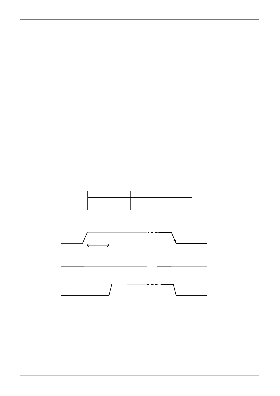
・Bit Transfer
SCL transfers 1-bit data during H. SCL cannot change signal of SDA during H at the time of bit transfer. If SDA changes
while SCL is H, START conditions or STOP conditions will occur and it will be interpreted as a control signal.
SDA
SCL
Data lin e stable;
Data valid
Change of data
allowed
・START and STOP condition
When SDA and SCL are H, data is not transferred on the I
2
C- bus. This condition indicates, if SDA changes from H to L
while SCL has been H, it will become START (S) conditions, and an access start, if SDA changes from L to H while SCL
has been H, it will become STOP (P) conditions and an access end.
SDA
SCL
S P
START Condition
STOP Condition
・Acknowledge
It transfers data 8 bits each after the occurrence of START condition. A transmitter opens SDA after transfer 8bits data, and
a receiver returns the acknowledge signal by setting SDA to L.
DATA OUTPUT
BY TRANSMITTER
DATA OUTPUT
BY RECEIVER
SCL from maste
S
START condition
12 89
not acknowledge
acknowledge
clock pulse for
acknowledgement
www.rohm.com
© 2011 ROHM Co., Ltd. All rights reserved.
10/35
2011.04 - Rev.
A
BD6081GU,BD6081GVW
A A
A
A
A7 A6 A5A4A3A2A1A
A
A
_
S
2
Technical Note
・ Writing protocol
A register address is transferred by the next 1 byte that transferred the slave address and the write-in command. The 3rd
byte writes data in the internal register written in by the 2nd byte, and after 4th byte or, the increment of register address is
carried out automatically. However, when a register address turns into the last address (1Ah), it is set to 00h by the next
transmission. After the transmission end, the increment of the address is carried out.
*1 *1
D7 D6D5 D4D3 D2D1D0 D7 D6 D5 D4 D3 D2D1D0
X X X X X X X
S
R/W=0(write)
from m aste r to slave
from slave to master
register addressslave address
00
DATA
register address
increment
=acknowledge(SDA LOW)
=not acknowledge(SDA HIGH)
S=START condition
P=STOP condition
*1: Write Timing
DATA
register address
●Timing diagram
SDA
BUF
t
SU;DAT
t
CL
LOW
t
HD;STA
t
HD;DAT
S Sr P
t
t HIGH
t
HD;STA
SU;STA
t
t SU;STO
S
●Electrical Characteristics(Unless otherwise specified, Ta=25 ℃, VBAT=3.6V, VIO=1.8V)
Standard-mode Fast-mode
Min. Typ. Max. Min. Typ. Max.
【I
C BUS format】
Parameter Symbol
SCL clock frequency fSCL 0 - 100 0 - 400 kHz
LOW period of the SCL clock tLOW 4.7 - - 1.3 - - s
HIGH period of the SCL clock tHIGH 4.0 - - 0.6 - - s
Hold time (repeated) START condition
After this period, the first clock is generated
tHD;STA 4.0 - - 0.6 - - s
Set-up time for a repeated START condition tSU;STA 4.7 - - 0.6 - - s
Data hold time tHD;DAT 0 - 3.45 0 - 0.9 s
Data set-up time tSU;DAT 250 - - 100 - - ns
Set-up time for STOP condition tSU;STO 4.0 - - 0.6 - - s
Bus free time between a STOP
and START condition
BUF 4.7 - - 1.3 - - s
t
P
Unit
www.rohm.com
© 2011 ROHM Co., Ltd. All rights reserved.
11/35
2011.04 - Rev.

A
BD6081GU,BD6081GVW
Technical Note
●Register List
Address
00h
01h
02h
03h
04h
05h
06h
07h
08h
09h
0Ah
0Bh
0Ch
0Dh
0Eh
0Fh
10h
11h
12h
13h
14h
15h
16h - - I1G2LED5 I1G2LED4 I1G2LED3 I1G2LED2 I1G2LED1 I1G2LED0 G2 LED current value1
17h
18h
19h
1Ah
1Dh
1Eh
1Fh
D7 D6 D5 D4 D3 D2 D1 D0
- - - - - - - SFTRST Software reset
- - REG2NML REG2PD - - - REG1PD Control LDO
- - SLEDSEL SLEDEN - - MLEDSEL MLEDEN Control Back Light
- - - IMLED4 IMLED3 IMLED2 IMLED1 IMLED0 Main Back Light current value
- - - ISLED4 ISLED3 ISLED2 ISLED1 ISLED0 Sub Back Light current value
- B2LEDMD G2LEDMD RGB2STA - B1LEDMD G1LEDMD RGB1STA
RGB1MD1 RGB1MD0 B1LEDPL G1LEDPL R1LEDPL B1LEDEN G1LEDEN R1LEDEN Control RGB1 LED
RGB1WT1TM3 RGB1WT1TM2 RGB1WT1TM1 RGB1WT1TM0 RGB1WT2TM3 RGB1WT2TM2 RGB1WT2TM1 RGB1WT2TM0 RGB1 ON time setting
RGB1SL1
STEP3
- - - - - RGB1SLNUM2 RGB1SLNUM1 RGB1SLNUM0 RGB1 slope step number setting
- - I1R1LED5 I1R1LED4 I1R1LED3 I1R1LED2 I1R1LED1 I1R1LED0 R1 LED current value1
- - IDLTR1LED5 IDLTR1LED4 IDLTR1LED3 IDLTR1LED2 IDLTR1LED1 IDLTR1LED0
- - I1G1LED5 I1G1LED4 I1G1LED3 I1G1LED2 I1G1LED1 I1G1LED0 G1 LED current value1
- - IDLTG1LED5 IDLTG1LED4 IDLTG1LED3 IDLTG1LED2 IDLTG1LED1 IDLTG1LED0
- - I1B1LED5 I1B1LED4 I1B1LED3 I1B1LED2 I1B1LED1 I1B1LED0 B1 LED current value1
- - IDLTB1LED5 IDLTB1LED4 IDLTB1LED3 IDLTB1LED2 IDLTB1LED1 IDLTB1LED0
RGB2MD1 RGB2MD0 B2LEDPL G2LEDPL R2LEDPL B2LEDEN G2LEDEN R2LEDEN Control RGB2 LED
RGB2WT1TM3 RGB2WT1TM2 RGB2WT1TM1 RGB2WT1TM0 RGB2WT2TM3 RGB2WT2TM2 RGB2WT2TM1 RGB2WT2TM0 RGB2 ON time setting
RGB2SL1
STEP3
- - - - - RGB2SLNUM2 RGB2SLNUM1 RGB2SLNUM0 RGB2 slope step number setting
- - I1R2LED5 I1R2LED4 I1R2LED3 I1R2LED2 I1R2LED1 I1R2LED0 R2 LED current value1
- - IDLTR2LED5 IDLTR2LED4 IDLTR2LED3 IDLTR2LED2 IDLTR2LED1 IDLTR2LED0
- - IDLTG2LED5 IDLTG2LED4 IDLTG2LED3 IDLTG2LED2 IDLTG2LED1 IDLTG2LED0
- - I1B2LED5 I1B2LED4 I1B2LED3 I1B2LED2 I1B2LED1 I1B2LED0 B2 LED current value1
- - IDLTB2LED5 IDLTB2LED4 IDLTB2LED3 IDLTB2LED2 IDLTB2LED1 IDLTB2LED0
- - - - - - RGB2MEL RGB1MEL
RGB1SL1
STEP2
RGB2SL1
STEP2
RGB1SL1
STEP1
RGB2SL1
STEP1
Input "0” for "-".
Prohibit to accessing the address that isn’t mentioned and the register for test.
Register data
Control RGB1, RGB2 LED
Setting GB LED connection
RGB1SL1
STEP0
RGB2SL1
STEP0
RGB1SL2
STEP3
RGB2SL2
STEP3
Reserved For test
Reserved For test
Reserved For test
RGB1SL2
STEP2
RGB2SL2
STEP2
RGB1SL2
STEP1
RGB2SL2
STEP1
RGB1SL2
STEP0
RGB2SL2
STEP0
RGB1 slope
1step time setting
current value
for R1 LED current step
current value
for G1 LED current step
current value
for B1 LED current step
RGB2 slope
1step time setting
current value
for R2 LED current step
current value
for G2 LED current step
current value
for B2 LED current step
RGB1, RGB2 LED
external ON/OFF control
Function
www.rohm.com
© 2011 ROHM Co., Ltd. All rights reserved.
12/35
2011.04 - Rev.
A
BD6081GU,BD6081GVW
●Register Map
Address 00h <Software reset>
BIT Name Initial
D7 - - - D6 - - - D5 - - - D4 - - - D3 - - - D2 - - - D1 - - - D0 SFTRST 0 Reset cancel Reset
Address 01h <Control LDO>
BIT Name Initial
D7 - - - D6 - - - D5 REG2NML 0 REG2 low current consumption mode REG2 normal mode
D4 REG2PD 0 REG2 power OFF REG2 power ON
D3 - - - D2 - - - D1 - - - D0 REG1PD 0 REG1 power OFF REG1 power ON
Address 02h <Control Back Light>
BIT Name Initial
D7 - - - D6 - - - D5 SLEDSEL 0 2 lights ON (SLED1~2) 1 lights ON (SLED1)
D4 SLEDEN 0 Sub Back Light OFF Sub Back Light ON
D3 - - - D2 - - - D1 MLEDSEL 0 4 lights ON (MLED1~4) 3 lights ON (MLED1~3)
D0 MLEDEN 0 Main Back Light OFF Main Back Light ON
0 1
0 1
0 1
Function
Function
Function
Technical Note
www.rohm.com
© 2011 ROHM Co., Ltd. All rights reserved.
13/35
2011.04 - Rev.

A
BD6081GU,BD6081GVW
Address 03h <Main Back Light current value>
BIT Name Initial
D7 - - - D6 - - - D5 - - - D4 IMLED4 0
D3 IMLED3 0 IMLED4 IMLED3 IMLED2 IMLED1 IMLED0 Current value
D2 IMLED2 0 0 0 0 0 0 1mA
D1 IMLED1 0 0 0 0 0 1 2mA
D0 IMLED0 0 0 0 0 1 0 3mA
・ ・ ・ ・ ・
・ ・ ・ ・ ・
・ ・ ・ ・ ・
1 1 1 0 1 30mA
1 1 1 1 0 31mA
1 1 1 1 1 32mA
When 120k is connected to ISET pin.
0 1
Function
Technical Note
1mA
Step
Address 04h <Sub Back Light current value>
BIT Name Initial
D7 - - - D6 - - - D5 - - - D4 ISLED4 0
D3 ISLED3 0
D2 ISLED2 0
D1 ISLED1 0
D0 ISLED0 0
ISLED4 ISLED3 ISLED2 ISLED1 ISLED0 Current value
0 0 0 0 0 1mA
0 0 0 0 1 2mA
0 0 0 1 0 3mA
・ ・ ・ ・ ・
・ ・ ・ ・ ・
・ ・ ・ ・ ・
1 1 1 0 1 30mA
1 1 1 1 0 31mA
1 1 1 1 1 32mA
When 120k is connected to ISET pin.
0 1
Function
1mA
Step
www.rohm.com
© 2011 ROHM Co., Ltd. All rights reserved.
14/35
2011.04 - Rev.

A
BD6081GU,BD6081GVW
Address 05h <Control RGB1, RGB2 LED, Setting GB LED connection>
BIT Name Initial
D7 - - - D6 B2LEDMD 0 B2LED connection =VBAT B2LED connection =VOUT
D5 G2LEDMD 0 G2LED connection =VBAT G2LED connection =VOUT
D4 RGB2STA 0 RGB2 LED Lighting stop RGB2 LED Lighting start
D3 - - - D2 B1LEDMD 0 B1LED connection =VBAT B1LED connection =VOUT
D1 G1LEDMD 0 G1LED connection =VBAT G1LED connection =VOUT
D0 RGB1STA 0 RGB1 LED Lighting stop RGB1 LED Lighting start
Address 06h <Control RGB1 LED>
BIT Name Initial
D7 RGB1MD1 0 Refer to the following Refer to the following
D6 RGB1MD0 0 Refer to the following Refer to the following
D5 B1LEDPL 0 Refer to the following Refer to the following
D4 G1LEDPL 0 Refer to the following Refer to the following
D3 R1LEDPL 0 Refer to the following Refer to the following
D2 B1LEDEN 0 B1 LED OFF B1 LED ON
D1 G1LEDEN 0 G1 LED OFF G1 LED ON
D0 R1LE DEN 0 R1 LED OFF R1 LED ON
RGB1MD1 RGB1MD0 *1LEDPL Mode
0 0 0 / 1 Normal 1
0 1 0 / 1 Normal 2
Address 07h <RGB1 ON time setting>
1 0
1 1
*1LEDPL : R1LEDPL, G1LEDPL, B1LEDPL is shown.
0 1
0 1
Function
Function
0 Blink 1
1 Blink 2
0 Slope 1
1 Slope 2
Technical Note
BIT Name Initial Function
D7 RGB1WT1TM3 0
D6 RGB1WT1TM2 0 RGB1WT1TM3 RGB1WT1TM2 RGB1WT1TM1 RGB1WT1TM0 Current light time
D5 RGB1WT1TM1 0 0 0 0 0 0.256s
D4 RGB1WT1TM0 0 0 0 0 1 0.512s
・
・
・
1 1 0 1 3.584s
D3 RGB1WT2TM3 0
D2 RGB1WT2TM2 0 RGB1WT2TM3 RGB1WT2TM2 RGB1WT2TM1 RGB1WT2TM0 Current light t ime
D1 RGB1WT2TM1 0 0 0 0 0 0.256s
D0 RGB1WT2TM0 0 0 0 0 1 0.512s
1 1 1 0 3.84s
1 1 1 1 4.096s
Lighting time depends on internal OSC frequency.
・
・
・
1 1 0 1 3.584s
1 1 1 0 3.84s
1 1 1 1 4.096s
Lighting time depends on internal OSC frequency.
・
・
・
・
・
・
・
・
・
・
・
・
・
・
・
・
・
・
0.256s
Step
0.256s
Step
www.rohm.com
© 2011 ROHM Co., Ltd. All rights reserved.
15/35
2011.04 - Rev.

A
BD6081GU,BD6081GVW
Address 08h <RGB1 slope 1step time setting>
BIT Name Initial Function
Technical Note
D7 RGB1SL1STEP3 0
D6 RGB1SL1STEP2 0
D5 RGB1SL1STEP1 0 0 0 0 0 4ms
D4 RGB1SL1STEP0 0 0 0 0 1 8ms
D3 RGB1SL2STEP3 0
D2 RGB1SL2STEP2 0
D1 RGB1SL2STEP1 0 0 0 0 0 4ms
D0 RGB1SL2STEP0 0 0 0 0 1 8ms
RGB1SL1
STEP3
・
・
・
1 1 0 1 56ms
1 1 1 0 60ms
1 1 1 1 64ms
Lighting time depends on internal OSC frequency.
RGB1SL2
STEP3
・
・
・
1 1 0 1 56ms
1 1 1 0 60ms
1 1 1 1 64ms
RGB1SL1
STEP2
・
・
・
RGB1SL2
STEP2
・
・
・
RGB1SL1
STEP1
RGB1SL2
STEP1
・
・
・
・
・
・
RGB1SL1
STEP0
RGB1SL2
STEP0
・
・
・
・
・
・
Current light time
4ms
Step
Current light time
4ms
Step
Lighting time depends on internal OSC frequency.
Address 09h <RGB1 slope step number setting>
BIT Name Initial
D7 - - - D6 - - - D5 - - - D4 - - - D3 - -
D2 RGB1SLNUM2 0
D1 RGB1SLNUM1 0 RGB1SLNUM2 RGB1SLNUM1 RGB1SLNUM0 Step
D0 RGB1SLNUM0 0 0 0 0 1 Step
0 0 1 2 Step
0 1
0 1 0 4 Step
0 1 1 8 Step
1 0 0 16 Step
1 0 1 32 Step
1 1 0 64 Step
1 1 1 (Prohibited)
Function
www.rohm.com
© 2011 ROHM Co., Ltd. All rights reserved.
16/35
2011.04 - Rev.

A
BD6081GU,BD6081GVW
Address 0Ah <R1 LED current value 1>
BIT Name Initial
D7 - - - D6 - - - D5 I1R1LED5 0
D4 I1R1LED4 0
D3 I1R1LED3 0
D2 I1R1LED2 0 0 0 0 0 0 1 0.5mA
D1 I1R1LED1 0 0 0 0 0 1 0 1mA
D0 I1R1LED0 0 ・ ・ ・ ・ ・ ・
Address 0Bh < current value for R1 LED current step>
BIT Name Initial
D7 - - - D6 - - - D5 IDLTR1LED5 0
D4 IDLTR1LED4 0
D3 IDLTR1LED3 0
D2 IDLTR1LED2 0 0 0 0 0 0 1 0.5mA
D1 IDLTR1LED1 0 0 0 0 0 1 0 1mA
D0 IDLTR1LED0 0 ・ ・ ・ ・ ・ ・
I1R1
LED5
0 0 0 0 0 0 0mA
・ ・ ・ ・ ・ ・
・ ・ ・ ・ ・ ・
・ ・ ・ ・ ・ ・
1 1 1 1 0 1 30.5mA
1 1 1 1 1 0 31mA
1 1 1 1 1 1 31.5mA
When 120k is connected to ISET pin.
IDL TR1
LED5
0 0 0 0 0 0 0mA
・ ・ ・ ・ ・ ・
・ ・ ・ ・ ・ ・
・ ・ ・ ・ ・ ・
1 1 1 1 0 1 30.5mA
1 1 1 1 1 0 31mA
1 1 1 1 1 1 31.5mA
0 1
I1R1
LED4
0 1
IDL TR1
LED4
I1R1
LED3
IDL TR1
LED3
Function
I1R1
LED2
Function
IDL TR1
LED2
I1R1
LED1
IDL TR1
LED1
I1R1
LED0
IDL TR1
LED0
Technical Note
Current value
0.5mA
Current value
0.5mA
Step
Step
www.rohm.com
© 2011 ROHM Co., Ltd. All rights reserved.
When 120k is connected to ISET pin.
17/35
2011.04 - Rev.

A
BD6081GU,BD6081GVW
Technical Note
Address 0Ch <G1 LED current value1>
BIT Name Initial
D7 - - - D6 - - - D5 I1G1LED5 0
D4
D3 I1G1LED3 0 0 0 0 0 0 0 0mA
D2 I1G1LED2 0 0 0 0 0 0 1 0.5mA
D1 I1G1LED1 0 0 0 0 0 1 0 1mA
D0 I1G1LED0 0 ・ ・ ・ ・ ・ ・
I1G1LED4 0
・ ・ ・ ・ ・ ・
I1G1
LED5
・ ・ ・ ・ ・ ・
・ ・ ・ ・ ・ ・
1 1 1 1 0 1 30.5mA
1 1 1 1 1 0 31mA
1 1 1 1 1 1 31.5mA
When 120k is connected to ISET pin.
0 1
I1G1
LED4
I1G1
LED3
Function
I1G1
LED2
I1G1
LED1
I1G1
LED0
Current
value
0.5mA
Address 0Dh < current value for G1 LED current step >
BIT Name Initial
D7 - - - D6 - - - D5 IDLTG1LED5 0
D4
D3 IDLTG1LED3 0 0 0 0 0 0 0 0mA
D2 IDLTG1LED2 0 0 0 0 0 0 1 0.5mA
D1 IDLTG1LED1 0 0 0 0 0 1 0 1mA
D0 IDLTG1LED0 0 ・ ・ ・ ・ ・ ・
IDLTG1LED4 0
・ ・ ・ ・ ・ ・
IDLTG1
LED5
・ ・ ・ ・ ・ ・
・ ・ ・ ・ ・ ・
1 1 1 1 0 1 30.5mA
1 1 1 1 1 0 31mA
1 1 1 1 1 1 31.5mA
When 120k is connected to ISET pin.
0 1
IDLTG1
LED4
IDLTG1
LED3
Function
IDLTG1
LED2
IDLTG1
LED1
IDLTG1
LED0
Current value
0.5mAStep
Step
www.rohm.com
© 2011 ROHM Co., Ltd. All rights reserved.
18/35
2011.04 - Rev.

A
BD6081GU,BD6081GVW
Address 0Eh <B1 LED Current value1>
BIT Name Initial
D7 - - - D6 - - - D5 I1B1LED5 0
D4
D3 I1B1LED3 0 0 0 0 0 0 0 0mA
D2 I1B1LED2 0 0 0 0 0 0 1 0.5mA
D1 I1B1LED1 0 0 0 0 0 1 0 1mA
D0 I1B1LED0 0 ・ ・ ・ ・ ・ ・
I1B1LED4 0
・ ・ ・ ・ ・ ・
I1B1
LED5
・ ・ ・ ・ ・ ・
・ ・ ・ ・ ・ ・
1 1 1 1 0 1 30.5mA
1 1 1 1 1 0 31mA
1 1 1 1 1 1 31.5mA
When 120k is connected to ISET pin.
0 1
I1B1
LED4
I1B1
LED3
Function
I1B1
LED2
I1B1
LED1
I1B1
LED0
Technical Note
Current value
0.5mA
Address 0Fh < current value for B1 LED current step >
BIT Name Initial
D7 - - - D6 - - - D5 IDLTB1LED5 0
D4
D3 IDLTB1LED3 0 0 0 0 0 0 0 0mA
D2 IDLTB1LED2 0 0 0 0 0 0 1 0.5mA
D1 IDLTB1LED1 0 0 0 0 0 1 0 1mA
D0 IDLTB1LED0 0 ・ ・ ・ ・ ・ ・
IDLTB1LED4 0
・ ・ ・ ・ ・ ・
IDLTB1
LED5
・ ・ ・ ・ ・ ・
・ ・ ・ ・ ・ ・
1 1 1 1 0 1 30.5mA
1 1 1 1 1 0 31mA
1 1 1 1 1 1 31.5mA
When 120k is connected to ISET pin.
0 1
IDLTB1
LED4
IDLTB1
LED3
Function
IDLTB1
LED2
IDLTB1
LED1
IDLTB1
LED0
Current value
0.5mA
Step
Step
www.rohm.com
© 2011 ROHM Co., Ltd. All rights reserved.
19/35
2011.04 - Rev.

A
BD6081GU,BD6081GVW
Address 10h <Control RGB2 LED>
BIT Name Initial
D7 RGB2MD1 0 Refer to following Refer to following
D6 RGB2MD0 0 Refer to following Refer to following
D5 B2LEDPL 0 Refer to following Refer to following
D4 G2LEDPL 0 Refer to following Refer to following
D3 R2LEDPL 0 Refer to following Refer to following
D2 B2LEDEN 0 B2 LED OF F B2 LED ON
D1 G2LEDEN 0 G2 LED OFF G2 LED ON
D0 R2LEDEN 0
RGB2MD1 RGB2MD0 *2LEDPL Mode
0 0 0 / 1 Normal 1
0 1 0 / 1 Normal 2
1 0
1 1
*2LEDPL : R2LEDPL, G2LEDPL, B2LEDPL is shown.
Address 11h <RGB2 ON time setting>
0 1
R2 LED OFF R2 LED ON
Function
0 Blink 1
1 Blink 2
0 Slope 1
1 Slope 2
Technical Note
BIT Name
D7 RGB2WT1TM3 0
D6 RGB2WT1TM2 0
D5 RGB2WT1TM1 0 0 0 0 0 0.256s
D4 RGB2WT1TM0 0 0 0 0 1 0.512s
D3 RGB2WT2TM3 0
D2 RGB2WT2TM2 0
D1 RGB2WT2TM1 0 0 0 0 0 0.256s
D0 RGB2WT2TM0 0 0 0 0 1 0.512s
Initial Function
RGB2WT1
TM3
・
・
・
1 1 0 1 3.584s
1 1 1 0 3.845s
1 1 1 1 4.096s
RGB2WT2
TM3
・
・
・
1 1 0 1 3.584s
1 1 1 0 3.845s
1 1 1 1 4.096s
RGB2WT1
TM2
・
・
・
Lighting time depends on internal OSC frequency.
RGB2WT2
TM2
・
・
・
Lighting time depends on internal OSC frequency.
RGB2WT1
TM1
・
・
・
RGB2WT2
TM1
・
・
・
RGB2WT1
TM0
・
・
・
RGB2WT2
TM0
・
・
・
Current ON time
setting
0.256s
Step
Current ON time
setting
0.256s
Step
www.rohm.com
© 2011 ROHM Co., Ltd. All rights reserved.
20/35
2011.04 - Rev.

A
BD6081GU,BD6081GVW
Address 12h <RGB2 slope 1step time setting>
Technical Note
BIT
D7 RGB2SL1STEP3 0
D6 RGB2SL1STEP2 0
D5 RGB2SL1STEP1 0 0 0 0 0 4ms
D4 RGB2SL1STEP0 0 0 0 0 1 8ms
D3 RGB2SL2STEP3 0
D2 RGB2SL2STEP2 0
D1 RGB2SL2STEP1 0 0 0 0 0 4ms
D0 RGB2SL2STEP0 0 0 0 0 1 8ms
Name Initial Function
RGB2SL1STEP3 RGB2SL1STEP2 RGB2SL1STEP1 RGB2SL1STEP0
・
・
・
1 1 0 1 56ms
1 1 1 0 60ms
1 1 1 1 64ms
Lighting time depends on internal OSC frequency.
RGB2SL2STEP3 RGB2SL2STEP2 RGB2SL2STEP1 RGB2SL2STEP0
・
・
・
1 1 0 1 56ms
1 1 1 0 60ms
1 1 1 1 64ms
Lighting time depends on internal OSC frequency.
・
・
・
・
・
・
・
・
・
・
・
・
・
・
・
・
・
・
Current ON time setting
4ms
Step
Current ON time setting
4ms
Step
Address 13h <RGB2 slope step number setting>
BIT Name Initial
D7 - - - D6 - - - D5 - - - D4 - - - D3 - -
D2 RGB2SLNUM2 0
D1 RGB2SLNUM1 0 RGB2SLNUM2 RGB2SLNUM1 RGB2SLNUM0 Step
D0 RGB2SLNUM0 0 0 0 0 1 Step
0 0 1 2 Step
0 1
0 1 0 4 Step
0 1 1 8 Step
1 0 0 16 Step
1 0 1 32 Step
1 1 0 64 Step
1 1 1 (Prohibited)
Function
www.rohm.com
© 2011 ROHM Co., Ltd. All rights reserved.
21/35
2011.04 - Rev.
A
BD6081GU,BD6081GVW
Technical Note
Address 14h <R2 LED current value1>
BIT Name Initial
D7 - - - D6 - - - D5 I1R2LED5 0
D4 I1R2LED4 0 I1R2LED5 I1R2LED4 I1R2LED3 I1R2LED2 I1R2LED1 I1R2LED0 Current value
D3 I1R2LED3 0 0 0 0 0 0 0 0mA
D2 I1R2LED2 0 0 0 0 0 0 1 0.5mA
D1 I1R2LED1 0 0 0 0 0 1 0 1mA
D0 I1R2LED0 0 ・ ・ ・ ・ ・ ・
・ ・ ・ ・ ・ ・
・ ・ ・ ・ ・ ・
・ ・ ・ ・ ・ ・
1 1 1 1 0 1 30.5mA
1 1 1 1 1 0 31mA
1 1 1 1 1 1 31.5mA
When 120k is connected to ISET pin.
0 1
Function
0.5mA
Address 15h < current value for R2 LED current step >
BIT Name Initial
D7 - - - D6 - - - D5 IDLTR2LED5 0
D4 IDLTR2LED4 0
D3 IDLTR2LED3 0 0 0 0 0 0 0 0mA
D2 IDLTR2LED2 0 0 0 0 0 0 1 0.5mA
D1 IDLTR2LED1 0 0 0 0 0 1 0 1mA
D0 IDLTR2LED0 0 ・ ・ ・ ・ ・ ・
・ ・ ・ ・ ・ ・
IDLTR2
LED5
・ ・ ・ ・ ・ ・
・ ・ ・ ・ ・ ・
1 1 1 1 0 1 30.5mA
1 1 1 1 1 0 31mA
1 1 1 1 1 1 31.5mA
When 120k is connected to ISET pin.
0 1
IDL TR2
LED4
IDL TR2
LED3
Function
IDL TR2
LED2
IDL TR2
LED1
IDL TR2
LED0
Current
value
0.5mA
Step
Step
www.rohm.com
© 2011 ROHM Co., Ltd. All rights reserved.
22/35
2011.04 - Rev.

A
BD6081GU,BD6081GVW
Technical Note
Address 16h <G2 LED current value1>
BIT Name Initial
D7 - - - D6 - - - D5 I1G2LED5 0
D4 I1G2LED4 0
D3 I1G2LED3 0 0 0 0 0 0 0 0mA
D2 I1G2LED2 0 0 0 0 0 0 1 0.5mA
D1 I1G2LED1 0 0 0 0 0 1 0 1mA
D0 I1G2LED0 0 ・ ・ ・ ・ ・ ・
・ ・ ・ ・ ・ ・
Address 17h < current value for G2 LED current step >
BIT Name Initial
D7 - - - D6 - - - D5 IDLTG2LED5 0
D4 IDLTG2LED4 0
D3 IDLTG2LED3 0
D2 IDLTG2LED2 0 0 0 0 0 0 1 0.5mA
D1 IDLTG2LED1 0 0 0 0 0 1 0 1mA
D0 IDLTG2LED0 0 ・ ・ ・ ・ ・ ・
I1G2LED5 I1G2LED4 I1G2LED3 I1G2LED2 I1G2LED1 I1G2LED
・ ・ ・ ・ ・ ・
・ ・ ・ ・ ・ ・
1 1 1 1 0 1 30.5mA
1 1 1 1 1 0 31mA
1 1 1 1 1 1 31.5mA
IDLTG2
LED5
0 0 0 0 0 0 0mA
・ ・ ・ ・ ・ ・
・ ・ ・ ・ ・ ・
・ ・ ・ ・ ・ ・
1 1 1 1 0 1 30.5mA
1 1 1 1 1 0 31mA
1 1 1 1 1 1 31.5mA
0 1
When 120k is connected to ISET pin.
0 1
IDLTG2
LED4
IDLTG2
LED3
Function
Function
IDLTG2
LED2
IDLTG2
LED1
0
IDLTG2
LED0
Current value
0.5mA
Current
value
0.5mA
Step
Step
www.rohm.com
© 2011 ROHM Co., Ltd. All rights reserved.
When 120k is connected to ISET pin.
23/35
2011.04 - Rev.

A
BD6081GU,BD6081GVW
Address 18h <B2 LED current value1>
BIT Name Initial
D7 - - - D6 - - - D5 I1B2LED5 0
D4 I1B2LED4 0 I1B2LED5 I1B2LED4 I1B2LED3 I1B2LED2 I1B2LED1 I1B2LED0 Current value
D3 I1B2LED3 0 0 0 0 0 0 0 0mA
D2 I1B2LED2 0 0 0 0 0 0 1 0.5mA
D1 I1B2LED1 0 0 0 0 0 1 0 1mA
D0 I1B2LED0 0 ・ ・ ・ ・ ・ ・
・ ・ ・ ・ ・ ・
・ ・ ・ ・ ・ ・
・ ・ ・ ・ ・ ・
1 1 1 1 0 1 30.5mA
1 1 1 1 1 0 31mA
1 1 1 1 1 1 31.5mA
0 1
When 120k is connected to ISET pin.
Function
Technical Note
0.5mA
Address 19h < current value for B2 LED current step >
BIT Name Initial
D7 - - - D6 - - - D5 IDLTB2LED5 0
D4 IDLTB2LED4 0
D3 IDLTB2LED3 0 0 0 0 0 0 0 0mA
D2 IDLTB2LED2 0 0 0 0 0 0 1 0.5mA
D1 IDLTB2LED1 0 0 0 0 0 1 0 1mA
D0 IDLTB2LED0 0 ・ ・ ・ ・ ・ ・
・ ・ ・ ・ ・ ・
IDLTB2
LED5
・ ・ ・ ・ ・ ・
・ ・ ・ ・ ・ ・
1 1 1 1 0 1 30.5mA
1 1 1 1 1 0 31mA
1 1 1 1 1 1 31.5mA
0 1
IDLTB2
LED4
IDLTB2
LED3
When 120k is connected to ISET pin.
Function
IDLTB2
LED2
IDLTB2
LED1
IDLTB2
LED0
Current value
0.5mA
Step
Step
Address 1Ah <RGB1, RGB2 LED external ON/OFF control>
BIT Name Initial
D7 - - - D6 - - - D5 - - - D4 - - - D3 - - - D2 - - - D1 RGB2MEL 0
D0 RGB1MEL 0 RGB*MEL RGB*CNT (external pin) RGB* LED Lighting
0 L ON
www.rohm.com
© 2011 ROHM Co., Ltd. All rights reserved.
Function
0 1
0 H ON
1 L OFF
1 H ON
But, a state of lighting depends on the setup of other registers.
24/35
2011.04 - Rev.
A
BD6081GU,BD6081GVW
●RGB LED operating
1. Operating mode
RGB LED can set up the following operating mode by the setup of the register.
<Setup register>
I1**LED : (register) Initial electric current value [mA]
IDLT**LED : (register) The electric current value of around 1Step [mA]
RGB*SLNUM : (register) slope step number (1,2,4,8,16,32,64 Step)
RGB*SL1STEP : (register) The first half slope 1Step time [ms]
RGB*SL2STEP : (register) The latter half slope 1Step time [ms]
RGB*WT1TM : (register) The first half lighting time [ms]
RGB*WT2TM : (register) The latter half lighting time [ms]
As for the following setup, calculate it from the ab ove setup.
I2**LED : At the time of middle lighting current value [mA] = I1**LED + IDLT**LED x RGB*SLNUM
(In case of the value that a calculation exceeds maximum value, the current value is at the limit with maximum.)
RGB*SL1TM : The first half slope time [ms] = RGB*SL1STEP x RGB*SLNUM
RGB*SL2TM : The latter half slope time [ms] = RGB*SL2STEP x RGB*SLNUM
Each setup is necessary for DC current (at Normal mode or Blink mode).
(* : 1/ 2 channels is shown. ** : R1/G1/B1/R2 /G2/B2 is shown.)
Note) The current value in the table, it is value when 120k is connected to ISET pin.
Normal mode 1
31.5mA
0mA
RGB*STA=1 RGB*STA=0
I1**LED
Time
Normal mode 2
31.5mA
I2**LED
I2**LED is a calculation.
0mA
RGB*STA=1 RGB*STA=0
Time
Technical Note
www.rohm.com
© 2011 ROHM Co., Ltd. All rights reserved.
25/35
2011.04 - Rev.
A
BD6081GU,BD6081GVW
Blink mode 1
31.5mA
RGB*WT1TM RGB*WT2TM
0mA
I1**LED
RGB*STA=1
Blink mode 2
31.5mA
RGB*WT1TM RGB*WT2TM
I2**LED
0mA
RGB*STA=1
Slope mode 1
31.5mA
RGB*SL1STEP
0mA
IDL T**LED
I1**LED
RGB*STA=1
RGB*SLNUM Step
Slope mode 2
31.5mA
RGB*WT1TM RGB*SL2TM RGB*SL1TM RGB*WT2TM
0mA
RGB*STA=1
RGB*SL1STEP
I1**LED
RGB*SLNUM Step
RGB*WT1TM/RGB*WT2TM is repeated.
I2**LED
RGB*STA=0
I2**LED is a calculation.
RGB*WT1TM/RGB*WT2TM is repeated.
I1**LED
RGB*STA=0
I2**LED,RGB*SL1TM,RGB*SL2TM is a calculation.
Until it becomes RGB*STA=0, Slope control is repeated.
RGB*WT1TM RGB*SL2TM RGB*SL1TM RGB*WT2TM
I2**LED
RGB*SL2STEP
IDL T**LED
RGB*SLNUM Step
I2**LED,RGB*SL1TM,RGB*SL2TM is a calculation.
Until it becomes RGB*STA=0, Slope control is repeated.
IDL T**LED
I2**LED
IDL T**LED
RGB*SL2STEP
RGB*SLNUM Step
Technical Note
Time
Time
Time
RGB*STA=0
Time
RGB*STA=0
www.rohm.com
© 2011 ROHM Co., Ltd. All rights reserved.
26/35
2011.04 - Rev.

A
BD6081GU,BD6081GVW
(A)
(B) (B) (C)
Technical Note
External pin control
31.5mA
RGB*WT1TM
RGB*WT2TM
0mA
I1**LED
I2**LED
RGB*STA=1 RGB*STA=0
Time
RGB*MEL
(register)
RGB*CNT
(External pin)
When RGB*MEL =0,
lighting
RGB*MEL=1 and RGB*CNT=H,
Lighting.
When RGB*MEL=0,
lighting
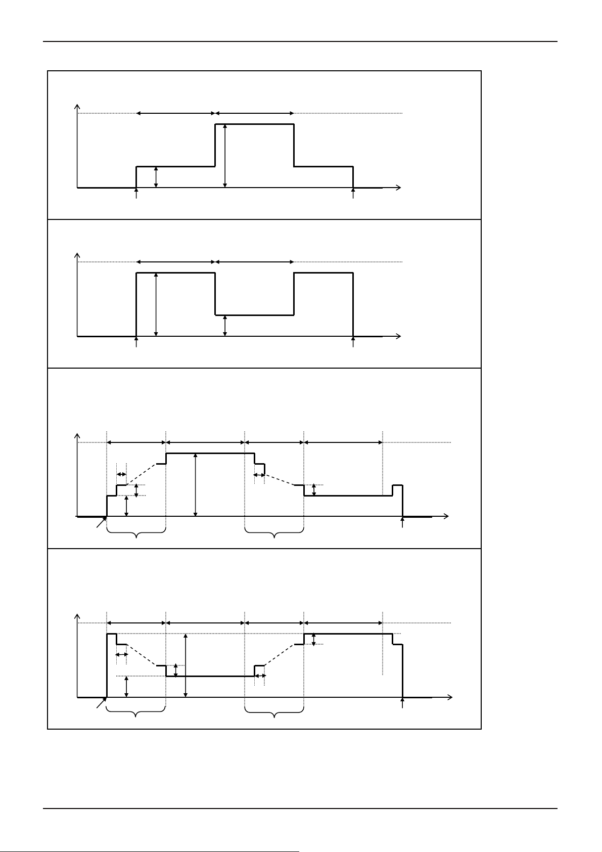
2. Slope control
The slope control that this LSI is equipped processes step ti me inside as follows.
It is made to have electric current by the log curve that is a simple target as to the slope.
RGB*STA
IDLT**LED
I1**LED
LED
current
T1
T2
T3
T4
T5
T7
T6
T8
(A)Section : It transits at the step time of two times when it was set up with RGB*SL1STEP
(B)Section : It transits at the step time when it was set up with RGB*SL1STEP.
(C)Section : It transits at the step time of a half times when it was set up with RGB*SL1STEP.
The time of the total (RGB*SL1TM) is calculated with RGB*SL1STEP x RGB*SLNUM.
A similar movement is done on the descent (RGB*SL2TM) side as well.
The acceptance of the setup of a register concerned with LED working during the slope movement stops.
But, a RGB*STA signal interrupts even during the slope movement, and it is possible that LED is turned off.
www.rohm.com
© 2011 ROHM Co., Ltd. All rights reserved.
27/35
2011.04 - Rev.

A
BD6081GU,BD6081GVW
●Explanation for operate
1. Reset
There are two kinds of reset, software reset and hardware reset.
(1) Software reset
・All the registers are initialized more than making a register (SFTRST) setup "1".
・The register of software resetting is an automatic return (Auto Return 0).
(2) Hardware reset
・It shifts to hardware reset by changing RESET pin “H” “L”.
・The condition of all the registers under hardware reset pi n is returned to the initial value,
and it stops accepting all address.
・It’s possible to release from a state of hardware reset by setting register “L” “H”.
・RESET pin has delay circuit. It doesn’t recognize as hardware reset in “L” period under 5s.
(3) Reset Sequence
・When hardware reset was done during software reset, software reset is canceled when
hardware reset is canceled. (Because the initial value of software reset is “0”)
2. Thermal shutdown
The blocks which thermal shutdown function is effective in the following.
Charge pump
LED Driver
REG1
REG2 is not shut down by thermal shutdown function, because REG2 can be used for I/O voltage.
A thermal shutdown function works in about 195
Detection temperature has a hysteresis, and detection rel ease temperature is about 175
(Design reference value)
℃.
Technical Note
℃.
www.rohm.com
© 2011 ROHM Co., Ltd. All rights reserved.
28/35
2011.04 - Rev.

A
BD6081GU,BD6081GVW
V
3. DC/DC
Start up
DC/DC circuit operates when either LED turns ON.
(But, when LED connection is set to DC/DC output (VOUT) only.)
DC/DC circuit has soft start function to prevent a rush current.
VBAT and VIO sequence is as follow.
BAT
VIO
RESET
EN (*)
VOUT
LED Current
(*) An EN signal means the following in the upper figure.
EN = “MLEDEN” or “SLEDEN” or “RGB1STA” or “RGB2STA”
(= LED The LED lighting control of a setup of connection VOUT)
But, as for VBAT < 2.2V (typ) or Ta > T
Mode transition
The transition of boosts multiple transits automatically by the VBAT voltage and the voltage of the LED electric current
inflow pin.
Condition:○
1
mode down=”H”
mode down=”H”
Over voltage protection / Over current protection
DC/DC circuit output (VOUT) is equipped with the over-voltage protection and the over current protection function.
A VOUT over-voltage detection voltage is about 6.0V.
A detection voltage has a hysteresis, and a detection release voltage is about 5.75V. (Design reference value)
And, when VOUT output short-circuits in GND, drain electric current is controlled by an over current protection function.
T
VBATON
T
VIOON=min 0.1ms
T
RSTB=min 0.1ms
T
(typ : 195° C), a protection function functions, and an EN signal doesn't become effective.
TSD
STANDBY
MLEDEN=”1” or SLEDEN =”1” or RGB *STA=”1”
(But, LED connection= It is limited to the LED lighting co ntrol of a setup of VOUT.)
1
○
VBAT>2.2V(typ) and Ta<T
SOFT
VOUT>1.5V(typ) After it is detected, 128us(typ) wait
X1.0
mode up=”H”
X1.5
mode up=”H”
X2.0 CP x2.0mode
T
VBATOFF
T
VIOOFF=min 1ms
T
RST=min 0ms
SOFT
ALL off
and
CP x1.0 mode
CP x1.0 mo de
CP x1.5mode
TSD
(VOUT at the time of rise in a voltage)
Technical Note
www.rohm.com
© 2011 ROHM Co., Ltd. All rights reserved.
29/35
2011.04 - Rev.
A
BD6081GU,BD6081GVW
4. LED Driver
LED current value setting
LED maximum current value (White LED driver and RGB LED Driver common) can be established in the resistance
value RISET that it is connected to the ISET Pin.
A setting is shown in the following.
ILEDmax = 6.4 x 0.6 [V] / RISET [k] [A] (Typ) MLED1to4, SLED1to2
ILEDmax = 6.3 x 0.6 [V] / RISET [k] [A] (Typ) All RGB LED
The maximum setting of LED current is 32mA (MLED and SLED), 31.5mA (RGB) on the D range of the internal circuit.
LED current overload protection
ISET Pin is mount with the GND short detection function. LED current value prevents excessive LE D current from
flowing when ISET Pin becomes low impedance because it is shown with a formula of the former extension.
White LED Driver
The number of lighting of white LED can be set up by the register MLEDSEL and SLEDSEL (address02h).
The settlement of the number of lighting can be setup with follow.
Main LCD Back light
Sub LCD Back light
・・・3 Light (MLED1 ~ 3) or 4 Light (MLED1 ~ 4)
・・・1 Light (SLED1) or 2 Light (SLED1 ~ 2)
Connect the LED pin that isn't used to the ground.
RGB LED Driver
By register B*LEDMD and G*LEDMD (address05h), a place of connection of Green LED and Blue LED It can be set up
in VBAT or VOUT. When Vf is low, it is connected to VBAT, and it is possible that efficiency is raised.
When a VBAT connection is chosen, a feedback route to the DC/DC circuit is interrupted, and it works as a simple
constant current driver.
A write protect is given in the following address when "1" is written in the RGB*STA register.
Register A protected address
RGB1STA 06h ~ 0Fh
RGB2STA 10h ~ 19h
VBAT connection a start in the setup Sequence
RGB*STA
T
on
(Max:6ms)
VOUT
LED current
When the connection of LED is VBAT, only a LED driver turns it on, and a DC/DC circuit is turned off.
The LED pin which isn't used is to short to the ground.
But, the setup of a register concerned with LED that isn’t used is prohibited.
Technical Note
www.rohm.com
© 2011 ROHM Co., Ltd. All rights reserved.
30/35
2011.04 - Rev.
A
BD6081GU,BD6081GVW
Technical Note
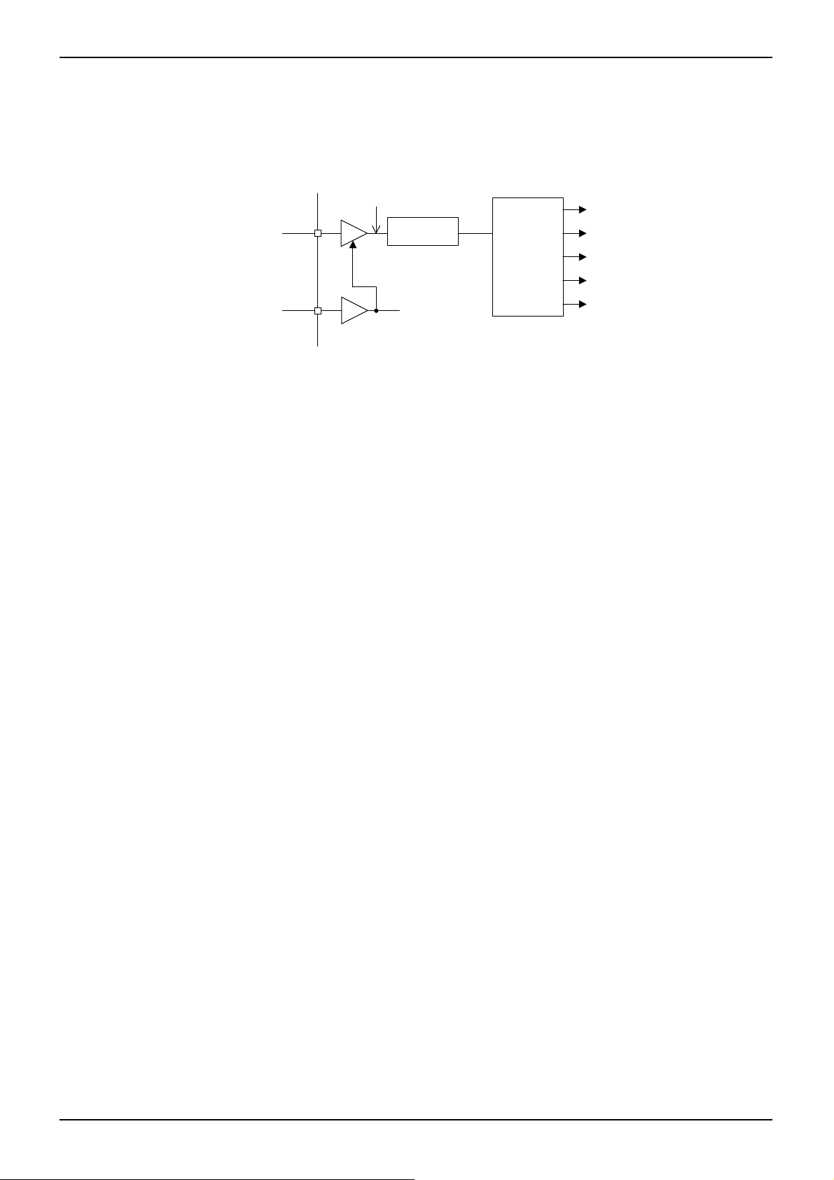
5. I/O
CPU interface control input is possible low voltage interface. Interface peripheral block diagram is as follows.
VIO voltage or interface voltage is possible the setting range of 1.65~3.3V. (But, VBAT voltage VIO voltage)
Also, I/O of with enable is being used for SCL, SDA input as a prevention of clock propagation to the inside when other LSI
shared the SCL, SDA line.
RESET=L, Output "H"
SCL
(SDA)
RESET
EN
Level shift
Logic
An equivalent circuit around the part I/O becomes p.8. By rising turn of the I/O power supply and the input level be careful
enough because an electric current route may occur through the protection Diode of the pin.
www.rohm.com
© 2011 ROHM Co., Ltd. All rights reserved.
31/35
2011.04 - Rev.

A
BD6081GU,BD6081GVW
A
6. About the start of REG2 (the voltage for I/O)
It must start as follows when REG2 output is used as VIO voltage.
VBAT (force)
RESET
(external pin control)
REG2EN
(external pin control)
REG2MD
(external pin control)
REG2O(output)
(=VIO voltage)
Min:7.5ms (*2)
Min:0ms (*4)
Technical Note
Low current
Stand By
(*1) This sequence is when REG2O is used as an I/O voltage.
(*2) When the low consumption mode is unnecessary, REG2EN=REG2MD (simultaneous control) is possible.
(*3) REG2 should go for a release of RESET at the time of the normal mode.
(*4) REG2EN= Though "L" and RESET= "L" don't care even about the simultaneous timing,
It is prohibition to take REG2EN= "L" in front of RESET= "L".
consumption mode
Min:2ms(*2)
Take the specifications of the outside power supply into consideration when the I/O voltage is applied from outside.
But, at that case as well, REG2 rising time in the normal mode Take a (Min : 2ms) into consideration.
Normal mode
Register access is possible (*3)
Stand By
It must start as follows when external power supply is used as VIO voltage.
VBAT(force)
VIO(force)
RESET(external pin control)
Register control
Impossible
VIO should go for a release of RESET after the time of the rising mode.
nd it is forbid to fall VIO before RESET=”L”.
Possible
Impossible
7. About the pin management of the function that isn't used and test pins
Please connect the pin that isn ’t used and test pin referred to equivalent circuit (P.8).
TESTI1, TESTI2 Short to GND (Must) because input pin for test
TESTO1, TESTO2 Be OPEN because out put for test
T1~T4 Short to GND (Must) because input pin for test
Non-used LED Pin Short to GND
But, the setup of a register concerned with LED that isn’t used is prohibited.
REG2EN, REG2MD, RGB1CNT, RGB2CNT Pull-Down resistance is built in.
Short to GND
www.rohm.com
© 2011 ROHM Co., Ltd. All rights reserved.
32/35
2011.04 - Rev.
A
BD6081GU,BD6081GVW
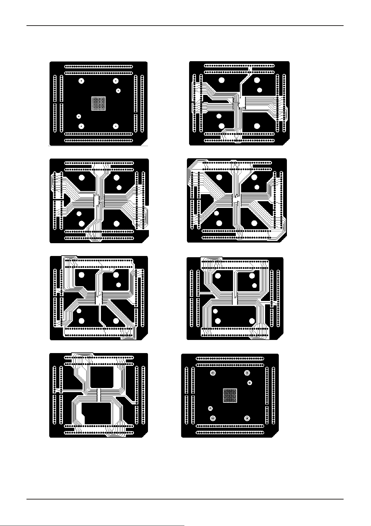
10. BD6081GU PCB pattern of the Power dissipation measuring board
Technical Note
1
st
layer(component) 2nd layer
3
rd
laye r 4th layer
5
th
layer 6th layer
th
layer 8th layer(solder)
7
www.rohm.com
© 2011 ROHM Co., Ltd. All rights reserved.
33/35
2011.04 - Rev.

A
BD6081GU,BD6081GVW
●Notes for use
(1) Absolute Maximum Ratings
An excess in the absolute maximum ratings, such as supply voltage, temperature range of operating conditions, etc., can
break down devices, thus making impossible to identif y breaking mode such as a short circuit or an open circuit. If any
special mode exceeding the absolute maximum ratings is a ssumed, consideration should be given to take physical safety
measures including the use of fuses, etc.
(2) Power supply and ground line
Design PCB pattern to provide low impedance for the wiring between the power supply and the ground lines. Pay attention
to the interference by common impedance of layout pattern when there are plural power supplies and ground lines.
Especially, when there are ground pattern for small signal and ground pattern for large current included the external
circuits, please separate each ground pattern. Furthermore, for all power supply pins to ICs, mount a capacitor between
the power supply and the ground pin. At the same time, in order to use a capacitor, thoroughly check to be sure the
characteristics of the capacitor to be used present no problem includin g the occurrence of capacity dropout at a low
temperature, thus determining the constant.
(3) Ground voltage
Make setting of the potential of the ground pin so that it will be maintained at the minimum in any operating state.
Furthermore, check to be sure no pins are at a potential lo wer than the ground voltage including an actual electric
transient.
(4) Short circuit between pins and erroneous mounting
In order to mount ICs on a set PCB, pay thorough attention to the direction and offset of the ICs. Erroneous mounting can
break down the ICs. Furthermore, if a short circuit occurs due to foreign matters entering between pins or between the pin
and the power supply or the ground pin, the ICs can break down.
Technical Note
(5) Operation in strong electromagnetic field
Be noted that using ICs in the strong electromagnetic field can malfunction them.
(6) Input pins
In terms of the construction of IC, parasitic elements are inevitably formed in relation to potential. The operation of the
parasitic element can cause interference with circuit operation, thus resulting in a malfunction and then breakdown of the
input pin. Therefore, pay thorough attention not to handle the input pins, such as to apply to the input pins a voltage lower
than the ground respectively, so that any parasitic element will operate. Furthermore, do not apply a voltage to the input
pins when no power supply voltage is applied to the IC. In addition, even if the power supply voltage is applied, apply to
the input pins a voltage lower than the power supply voltage or within the guarante ed value of electrical characteristics.
(7) External capacitor
In order to use a ceramic capacitor as the external capacitor, determine the constant with consideration given to a
degradation in the nominal capacitance due to DC bias and changes in the capacitance due to temperature, etc.
(8) Thermal shutdown circuit (TSD)
This LSI builds in a thermal shutdown (TSD) circuit. When junction temperatures become detection temperature or higher,
the thermal shutdown circuit operates and turns a switch OFF. The thermal shutdown circuit, which is aimed at isolating
the LSI from thermal runaway as much as possible, is not aimed at the protection or guarantee of the LSI. Therefore, do
not continuously use the LSI with this circuit operat ing or use the LSI assuming its operation.
(9) Thermal design
Perform thermal design in which there are adequate margins by taking into account the permissible dissipation (Pd) in
actual states of use.
(10) LDO
Use each output of LDO by the independence. Don’t use under the condition that each output is short-circuited because it
has the possibility that an operation becomes unstable.
(11) About the pin for the test, the un-use pin
Prevent a problem from being in the pin for the test and the un-use pin under the state of actual use. Please refer to a
function manual and an application noteboo k . And, as for the pin that doesn't specially have an explanation, ask our
company person in charge.
(12) About the function description or application note or more.
The function manual and the application notebook are the design materials to design a set. So, the cont ents of t he
materials aren't always guaranteed. Please design application by having fully examinati on and evaluation include the
external elements.
www.rohm.com
© 2011 ROHM Co., Ltd. All rights reserved.
34/35
2011.04 - Rev.

A
BD6081GU,BD6081GVW
●Ordering part number
B D 6 0 8 1 G U - E 2
Part No. Part No.
6081
VCSP85H3
(BD6081GU)
1PIN MARK
0.08
A
56 7
3.90± 0.1
1.0MAX
0.25±0.1
S
S
0.45±0.1
B
P=0.5× 6
(Unit : mm)
3.90±0.1
48-φ0.30±0.05
0.05
(φ0.15)INDEX POST
0.45±0.1
BA
G
F
E
D
C
B
A
1234
P=0.5× 6
SBGA063W060
1PIN MARK
6.0±0.1
0.1 S
P=0.65×7
63-φ0.33± 0.05
M
φ
0.08
0.65
ABS
H
G
F
E
D
C
B
A
6.0± 0.1
S
0.08
0.9MAX
0.725±0.1
A
B
0.65
51
3
762
4
P=0.65×7
8
0.725±0.1
(Unit : mm)
Package
GU : VCSP85H3
GVW : SBGA063W060
<Tape and Reel information>
Embossed carrier tapeTape
Quantity
Direction
of feed
<Tape and Reel information>
Quantity
Direction
of feed
2500pcs
E2
The direction is the 1pin of product is at the upper left when you hold
()
reel on the left hand and you pull out the tape on the right hand
Reel
Embossed carrier tape (with dry pack)Tape
2000pcs
E2
The direction is the 1pin of product is at the upper left when you hold
()
reel on the left hand and you pull out the tape on the right hand
Reel
1pin
Packaging and forming specification
E2: Embossed tape and reel
1pin
Order quantity needs to be multiple of the minimum quantity.
∗
Order quantity needs to be multiple of the minimum quantity.
∗
Direction of feed
Direction of feed
Technical Note
www.rohm.com
© 2011 ROHM Co., Ltd. All rights reserved.
35/35
2011.04 - Rev.

Notes
No copying or reproduction of this document, in part or in whole, is permitted without the
consent of ROHM Co.,Ltd.
The content specied herein is subject to change for improvement without notice.
The content specied herein is for the purpose of introducing ROHM's products (hereinafter
"Products"). If you wish to use any such Product, please be sure to refer to the specications,
which can be obtained from ROHM upon request.
Examples of application circuits, circuit constants and any other information contained herein
illustrate the standard usage and operations of the Products. The peripheral conditions must
be taken into account when designing circuits for mass production.
Great care was taken in ensuring the accuracy of the information specied in this document.
However, should you incur any damage arising from any inaccuracy or misprint of such
information, ROHM shall bear no responsibility for such damage.
The technical information specied herein is intended only to show the typical functions of and
examples of application circuits for the Products. ROHM does not grant you, explicitly or
implicitly, any license to use or exercise intellectual property or other rights held by ROHM and
other parties. ROHM shall bear no responsibility whatsoever for any dispute arising from the
use of such technical information.
The Products specied in this document are intended to be used with general-use electronic
equipment or devices (such as audio visual equipment, ofce-automation equipment, communication devices, electronic appliances and amusement devices).
The Products specied in this document are not designed to be radiation tolerant.
While ROHM always makes efforts to enhance the quality and reliability of its Products, a
Product may fail or malfunction for a variety of reasons.
Please be sure to implement in your equipment using the Products safety measures to guard
against the possibility of physical injury, re or any other damage caused in the event of the
failure of any Product, such as derating, redundancy, re control and fail-safe designs. ROHM
shall bear no responsibility whatsoever for your use of any Product outside of the prescribed
scope or not in accordance with the instruction manual.
The Products are not designed or manufactured to be used with any equipment, device or
system which requires an extremely high level of reliability the failure or malfunction of which
may result in a direct threat to human life or create a risk of human injur y (such as a medical
instrument, transportation equipment, aerospace machinery, nuclear-reactor controller, fuelcontroller or other safety device). ROHM shall bear no responsibility in any way for use of any
of the Products for the above special purposes. If a Product is intended to be used for any
such special purpose, please contact a ROHM sales representative before purchasing.
If you intend to export or ship overseas any Product or technology specied herein that may
be controlled under the Foreign Exchange and the Foreign Trade Law, you will be required to
obtain a license or permit under the Law.
Notice
www.rohm.com
© 2011 ROHM Co., Ltd. All rights reserved.
Thank you for your accessing to ROHM product informations.
More detail product informations and catalogs are available, please contact us.
ROHM Customer Support System
http://www.rohm.com/contact/
R1120
A
 Loading...