

System LED Drivers for Mobile phones
Chopper type
for Flash
BD6062GU
●Description
The BD6062GU is 1A Flash LED Driver ICs that can drive 1LED. It is possible to select how to control, 2wired control mode
(Direct Control Mode) or 3wired mode (Register Control Mode). The BD6062GU has original Timer function in 3wired mode
and easily set pre-flash timer and flash timer.
●Features
1) 400mA ~ 800mA selectable in Flash mode (Register Control Mode)
2) 50 ~ 200mA Torch mode (Register Control Mode)
3) 800mA in Flash mode (Direct control Mode)
4) 200mA in Torch mode (Direct control Mode)
5) Maximum current of LED is 1A in both Flash and Torch mode
6) 3Wired Mode and Direct control Mode selectable
7) In 3Wired Mode, Pre-Flash Timer and Flash Timer controllable
8) In 3Wired Mode, Flash current and Torch current is controllable
9) Over voltage protection
10) CSP 23pin Small and Thin package
●Applications
Flash and torch of camera for mobile phone
●Line up matrix
Parameter BD6062GU
Input voltage 2.7 ~ 5.5V
No.11041EBT13
Switching Frequency 480 ~ 720kHz
Maximum LED Current 1A
Package VCSP85H2
●Absolute maximum ratings (Ta=25℃)
Parameter Symbol Ratings Unit Condition
Maximum applied voltage VMAX 7 V VBAT, VIO
Power dissipation Pd 1100 *1 mW
Operating temperature range Topr -30~+85 ℃
Storage temperature range Tstg -55~+150 ℃
*1 50mm × 58mm × 1.75mm At glass epoxy board mounting. When it’s used by more than Ta=25℃, it’s reduced by 11mW/℃
●Recommended operating range (Ta= -30℃ ~ +85℃)
Parameter Symbol
Power Supply Voltage VDD 2.7 3.6 5.5 V *2
IO Supply Voltage VIO 1.62 1.8 3.3 V *
*2 VBAT VIO
Min. Typ. Max.
Ratings
Unit Condition
2
www.rohm.com
© 2011 ROHM Co., Ltd. All rights reserved.
1/15
2011.05 - Rev.B

BD6062GU
●Electrical characteristics
(Unless otherwise noted, Ta = +25℃, VBAT=3.6V, VIO=1.8V)
Parameter Symbol
[Logic control terminal (IFMODE=’L’, 3wired control mode)]
Low threshold voltage1 VthL1 - - VIO* 0.25 V
High threshold voltage1 VthH1 VIO* 0.75 - - V
High level Input current1 IinH1 - - 5 A Vin=VIO
Low level Input current1 IinL1 -5 - - A Vin=0V
[Logic control terminal (IFMODE=’H’, Direct control mode)]
Low threshold voltage2 VthL2 - - 0.4 V
High threshold voltage2 VthH2 1.4 - - V
High level Input current2 IinH2 - 18.3 30 A FLASH=TORCH=5.5V
Low level Input current2 IinL2 -2 -0.1 - A FLASH=TORCH=0V
Min. Typ. Max.
Limits
Units Condition
Technical Note
[Others]
Input voltage range Vin 3.1 - 5.5 V VBAT input range
Quiescent Current Iq - 5 10 A Torch=Flash= OFF
Current Consumption Idd1 - 1.8 2.5 mA
Inductor current limit Icoil 1.5 2.0 2.5 A Vin=3.6V *3
Switching frequency fSW 480 600 720 kHz
SW ON resistance Ron - 0.07 0.15 Iin=200mA
Duty cycle limit Duty 60 65 - % VFB=0V
Output voltage range Vo - - 5.4 V
Over voltage limit Ovl 5.4 5.5 5.6 V VFB=0V
Start up time Ts 0.5 1.0 ms 0mA to 200mA(Torch)
R torch terminal voltage 1 Vrt1 45 50 55 mV Itorch[1:0]=00 (50mA)
R torch terminal voltage 2 Vrt2 90 100 110 mV Itorch[1:0]=01 (100mA)
VFB=1.0V, Vin=3.6V,
Torch mode
R torch terminal voltage 3 Vrt3 135 150 165 mV Itorch[1:0]=10 (150mA)
R torch terminal voltage 4 Vrt4 180 200 220 mV Itorch[1:0]=11 (200mA)
R flash terminal voltage 1 Vrf1 43 48 53 mV Iflash[1:0]=00 (400mA)
R flash terminal voltage 2 Vrf2 54 60 66 mV Iflash[1:0]=01 (500mA)
R flash terminal voltage 3 Vrf3 65 72 79 mV Iflash[1:0]=10 (600mA)
R flash terminal voltage 4 Vrf4 86 96 106 mV Iflash[1:0]=11 (800mA)
*3 This parameter is tested with dc measurement.
www.rohm.com
© 2011 ROHM Co., Ltd. All rights reserved.
2/15
2011.05 - Rev.B
BD6062GU
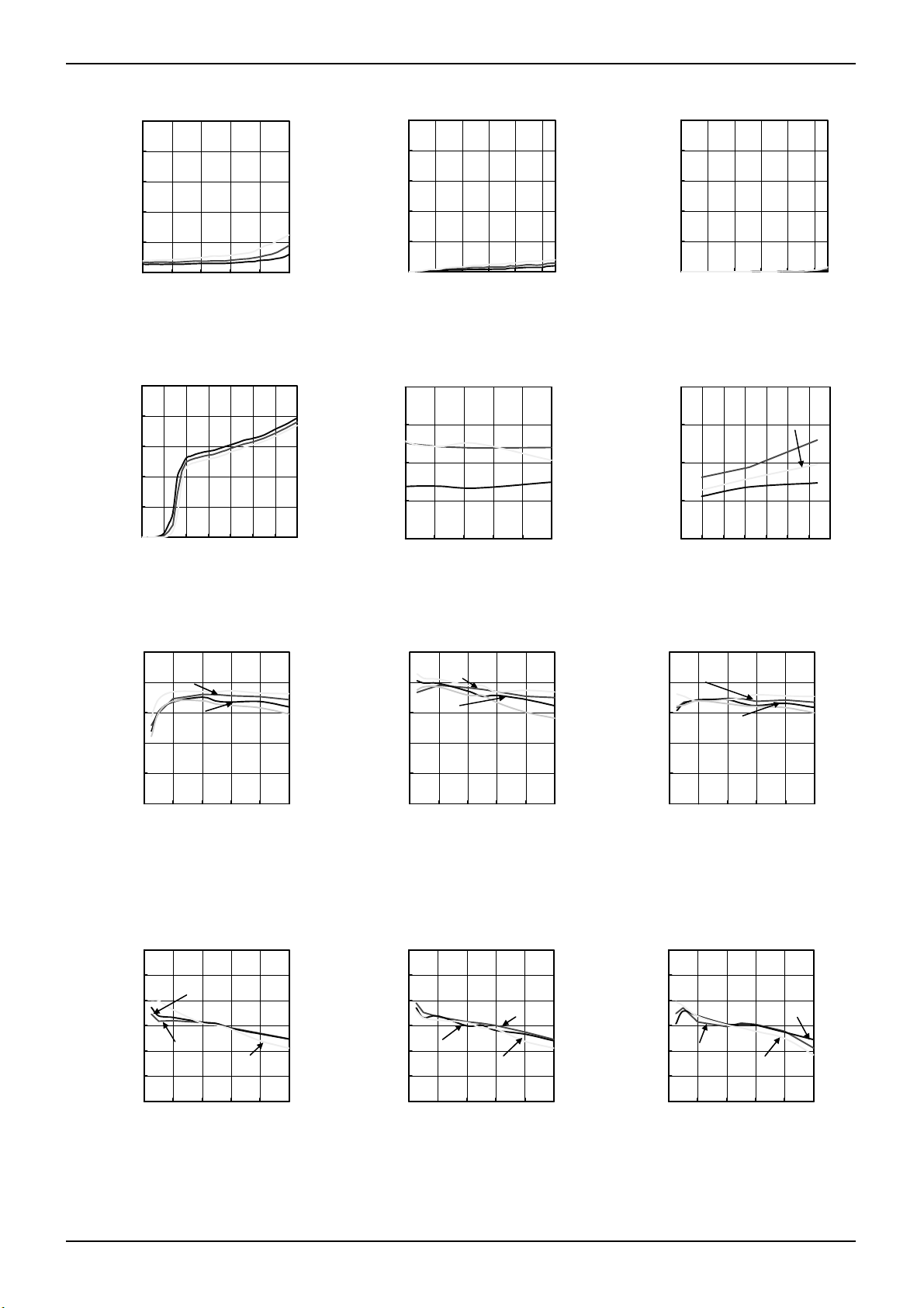
●Electrical characteristic curves (Reference data)
0.1
0.08
0.06
0.04
Ta= 8 5° C
0.02
STAND-BY CURRENT : lstb[A]
0
33.544.555.5
INPUT VOLTAGE : VBAT[V]
Ta= 2 5° C
Ta= - 30 °C
Fig.1 Quiescent current consumption
(VBAT)
Fig.2 Quiescent current consumption
3
2.4
1.8
1.2
0.6
CURRENT CONSUMPTION: ldd[mA]
0
01234567
INPUT VOLTAGE : VBAT[V]
Ta= 2 5° C
Ta= 8 5° C
Ta= - 30 °C
Fig.4 Current consumption(VBAT)
CURRENT LIMIT : llimit[A]
100
VBAT=3.6V
90
EFFICIENCY [%]
80
70
60
50
VBAT=3.0V
0 200 400 600 800 1000
LED CURRENT : ILED[mA]
VBAT=4.2V
VBAT=2.7V
Fig.7 1A appli. Efficiency
(Ta = 25°C)
100
EFFICIENCY [%]
95
90
85
80
75
70
TDK Coil
Taiyo Yuden Coil
Panasonic Coil
0 200 400 600 800 1000
LED CURRENT : ILED[mA]
Fig.10 Each Coil Efficiency
(Ta = 25°C, VBAT = 3.6V)
0.1
0.08
0.06
0.04
0.02
STAND-BY CURRENT: lstb_VIO[A]
0
012345
INPUT VOLTAGE : VBAT[V]
Ta= 8 5° C
Ta= 2 5° C
Ta= - 30 °C
(VIO)
2.5
2.25
2
1.75
1.5
33.544.555.5
INPUT VOLTAGE : VBAT[V]
Ta= 2 5° C
Ta= 8 5° C
Ta= - 30 °C
Fig.5 Over-Current Limiter
100
VBAT=3.6V
VBAT=3.0V
0 200 400 600 800 1000
LED CURRENT : ILED[mA]
EFFICIENCY [%]
90
80
70
60
50
VBAT=4.2V
VBAT=2.7V
Fig.8 1A appli. Efficiency
(Ta = 85°C)
100
95
90
85
TDK Coil
80
EFFICIENCY [%]
75
70
0 200 400 600 800 1000
LED CURRENT : ILED[mA]
Taiyo Yuden Coil
Panasonic Coil
Fig.11 Each Coil Efficiency
(Ta = 85°C, VBAT = 3.6V)
Technical Note
0.1
0.08
0.06
0.04
0.02
0
STAND-BY CURRENT : lstb_OVP[A]
012345
INPUT VOLTAGE : VBAT[V]
Fig.3 Quiescent current consumption
(OVP)
700
650
600
FSW[kHz]
550
SWITCHING FREQUENCY :
500
22.533.544.555.5
Ta= 2 5° C
INPUT VOLTAGE : VBAT[V]
Fig.6 Switching Frequency
100
VBAT=3.6V
90
EFFICIENCY [%]
80
70
60
50
VBAT=3.0V
0 200 400 600 800 1000
LED CURRENT : ILED[mA]
Fig.9 1A appli. Efficiency
(Ta = -30°C)
100
95
90
85
Taiyo Yuden Coil
80
EFFICIENCY [%]
75
70
0 200 400 600 800 1000
LED CURRENT : ILED[mA]
Fig.12 Each Coil Efficiency
(Ta = -30°C, VBAT = 3.6V)
Ta= 8 5° C
Ta= 2 5° C
Ta= - 30 °C
Ta= 8 5° C
Ta= - 30 °C
VBAT=4.2V
VBAT=2.7V
TDK Coil
Panasonic Coil
www.rohm.com
© 2011 ROHM Co., Ltd. All rights reserved.
3/15
2011.05 - Rev.B
BD6062GU
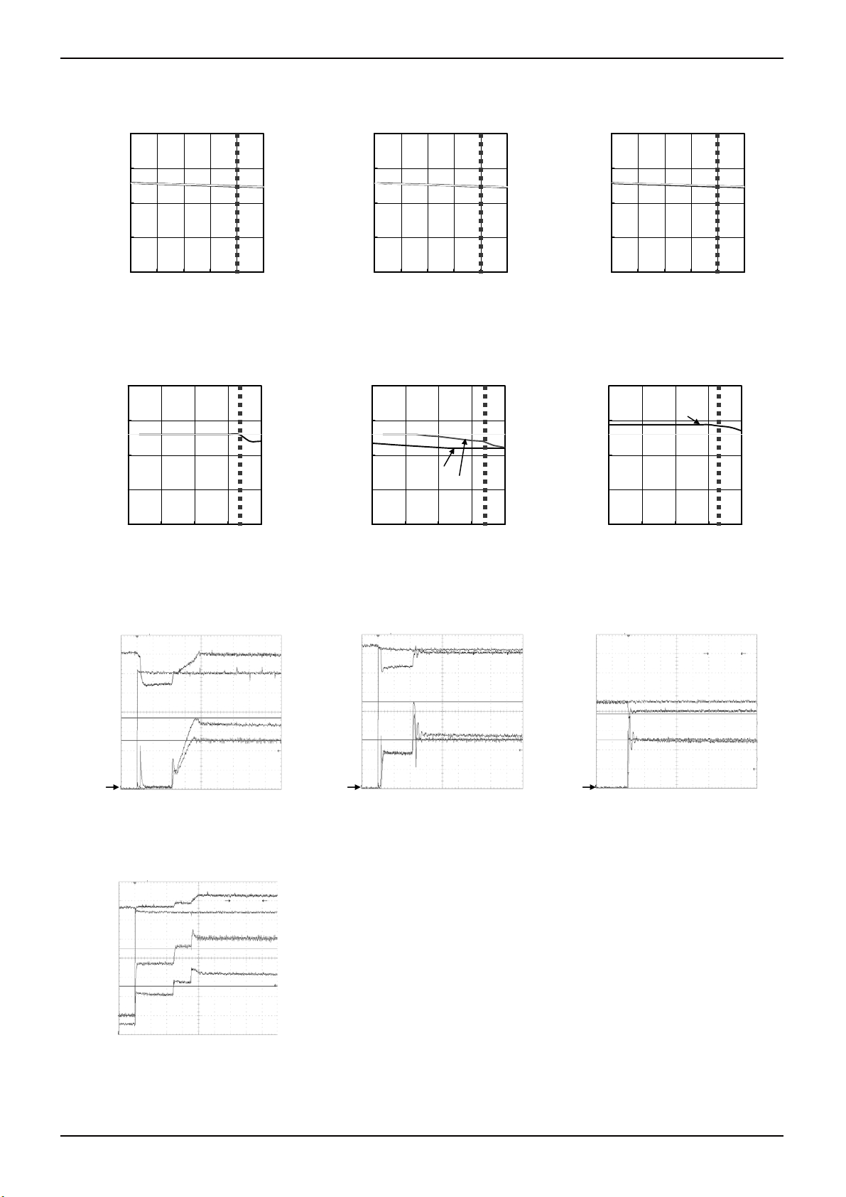
●Electrical characteristic curves (Reference data) – Continued
0.22
0.21
0.2
Ta= 8 5° C
Ta= 2 5° C
Ta= - 30 °C
0.22
0.21
0.2
Ta= 8 5° C
Ta= 2 5° C
Ta= - 30 °C
TFB VOLTAGE : VTFB[V]
0.19
0.18
0 50 100 150 200 250
TFB CURRENT : ITFB[mA]
0.19
TFB VOLTAGE: VTFB[V]
0.18
0 50 100 150 200 250
TFB CURRENT : ITFB[mA]
Fig.13 TORCH Load Regulation
(VBAT = 5.5V)
Fig.14 TORCH Load Regulation
(VBAT = 3.6V)
100
100
95
Ta= - 30 °C
90
85
FFB VOLTAGE : VFFB[mV]
80
0 300 600 900 1200
FFB CURRENT : IFFB[mA]
Fig.16 FLASH Load Regulation
(VBAT = 5.5V)
Ta= 2 5° C
Ta= 8 5° C
95
90
85
FFB VOLTAGE: VFFB[mV]
80
0 300 600 900 1200
FFB CURRENT : IFFB[mA]
Ta= - 30 °C
Ta= 8 5° C
Ta= 2 5° C
Fig.17 FLASH Load Regulation
(VBAT = 3.6V)
OUTPUT VOLTAGE [500mV/div]
TORCH/FLASH Terminal
(VBAT) [500mV/div]
INPUT CURRENT [200mA/div]
LED CURRENT
[200mA/div]
TORCH/FLASH Terminal
(VBAT) [500mV/div]
OUTPUT VOLTAGE
[500mV/div]
INPUT CURRENT
[200mA/div]
LED CURRENT
[200mA/div]
0V, 0A 0V, 0A 0V, 0A
200µs/div
200µs/div
Fig.19 500mA Input rush current
(VBAT=3.0V)
Fig.20 500mA Input rush current
(VBAT=3.6V)
OUTPUT VOLTAGE [500mV/div]
TORCH/FLASH Terminal
(VBAT) 500mV/div]
LED CURRENT
[200mA/div]
INPUT CURRENT
[500mA/div]
Fig.22 1A Input rush current
(200mA 1A)
Technical Note
0.22
0.21
0.2
0.19
TFB VOLTAGE: VTFB[V]
0.18
0 50 100 150 200 250
Fig.15 TORCH Load Regulation
100
95
Ta= - 30 °C
90
85
FFB VOLTAGE: VFFB[mV]
80
0 300 600 900 1200
TFB CURRENT : ITFB[mA]
Fig.18 FLASH Load Regulation
Fig.21 500mA Input rush current
Ta= 8 5° C
Ta= 2 5° C
Ta= - 30 °C
TFB CURRENT : ITFB[mA]
(VBAT = 2.7V)
Ta= 8 5° C
Ta= 2 5° C
(VBAT = 2.7V)
TORCH/FLASH Terminal
(VBAT) [1V/div]
OUTPUT VOLTAGE [1A/div]
INPUT CURRENT [200mA/div]
LED CURRENT [200mA/div]
200µs/div
(VBAT=4.5V)
www.rohm.com
© 2011 ROHM Co., Ltd. All rights reserved.
4/15
2011.05 - Rev.B
BD6062GU
A
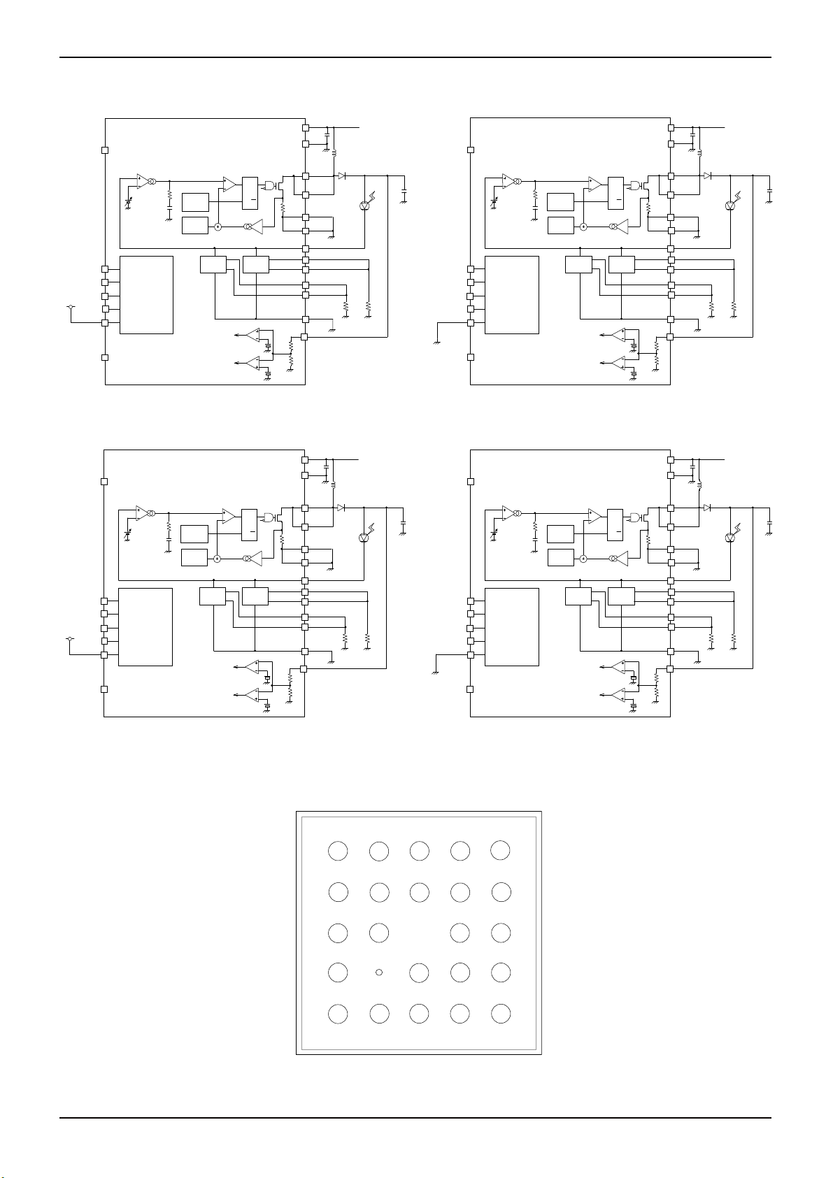
●Block diagram and pin configuration
VIO
osc
slope
Q
R
Q
S
TORCH (CS)
CLK
CSDI
FLASH
(RSTB)
IFMODE
TEST
Control
CURDRV
TORCH
OPEN
OVP
CURDRV
FLASH
Fig.23 1A application Block diagram of
Direct control Mode
VIO
Q
osc
slope
R
S
Q
TORCH (CS)
CLK
CSDI
FLASH
(RSTB)
IFMODE
TEST
Control
CURDRV
TORCH
OPEN
OVP
CURDRV
FLASH
Fig.25 500mA application Block diagram of
Direct control Mode
Technical Note
R
S
CURDRV
FLASH
R
S
CURDRV
FLASH
VBAT
2.2µF
(6.3V)
GND
SW1
Q
Q
Q
Q
SW2
PGND1
PGND2
VFB
RFLASH
FFB
RTORCH
TFB
GNDSENS
OVP
VBAT
4.7µF
(6.3V)
GND
SW1
SW2
PGND1
PGND2
VFB
RFLASH
FFB
RTORCH
TFB
GNDSENS
OVP
4.7µH
SBD
1 0.12
4.7µH
SBD
2 0.24
Battery
Battery
47µF
(6.3V)
22µF
(6.3V)
VBAT
2.2µF
(6.3V)
GND
SW1
SW2
PGND1
PGND2
VFB
RFLASH
FFB
RTORCH
TFB
GNDSENS
OVP
4.7µH
SBD
1 0.12
Battery
47µF
(6.3V)
TORCH (CS)
RSTB
(FLASH)
IFMODE
CSDI
TEST
VIO
osc
slope
CURDRV
TORCH
CLK
Control
OVP
OPEN
Fig.24 1A application Block diagram of
3wired control Mode
22µF
(6.3V)
VIO
osc
slope
CURDRV
TORCH (CS)
CLK
CSDI
FLASH
(RSTB)
IFMODE
TEST
Control
TORCH
OVP
OPEN
VBAT
4.7µF
(6.3V)
GND
SW1
SW2
PGND1
PGND2
VFB
RFLASH
FFB
RTORCH
TFB
GNDSENS
OVP
Battery
4.7µH
SBD
2 0.24
Fig.26 500mA application Block diagram of
3wired control Mode
5
4
3
2
B
N.C.
GND
SENS
FTB
RSTB/
FLASH
SW2
SW1
IFMODE
C
VIO
CSDI
TFB
D E
PGND2
PGND1
OVP
TORCH
N.C.
CLK
VBAT
CS/
GND
1
TEST
RFLASH
VFB
RTORCH
N.C.
Fig.27 pin location diagram (TOP VIEW)
www.rohm.com
© 2011 ROHM Co., Ltd. All rights reserved.
5/15
2011.05 - Rev.B

BD6062GU
●Pin assignment table
No. Pin Name
In/
Out
Functions
A1 TEST In Digital test select pin
A2 RSTB/FLASH In
Reset (“L”:Reset) (IFMODE=’0’)
FLASH enable (“H”) (IFMODE=’1’)
A3 FFB In Flash current driver feedback pin
A4 GNDSENS In Sense GND pin for current driver
A5 N.C - open
B1 RFLASH Out Flash current adjustment resistor pin
B3 IFMODE In Interface mode select
B4 SW1 In Switching terminal 1
B5 SW2 In Switching terminal 2
C1 VFB In Voltage feedback pin
C2 TFB In Torch current driver feedback pin
C4 CSDI In Data input
C5 VIO - I/O power supply pin
D1 RTORCH Out Torch current adjustment resistor pin
D2 CS/TORCH In
Chip select (IFMODE=’0’)
TORCH enable (IFMODE=’1’)
D3 OVP In Boost voltage feedback input pin
D4 PGND1 - Power GND pin 1
D5 PGND2 - Power GND pin 2
E1 N.C - Open
E2 GND - GND pin
E3 VBAT - Battery power supply pin
E4 CLK In Clock
E5 N.C - Open
Total : 23 Pin
●Description of function
1) CPU I/F
The Control Serial I/F provides access to Flash LED driver control registers.
Write timing show following timing chart.
CLK
t
t
sFS
hFS
Duty
Technical Note
CS
t
hDI
sDI
CSDI
A7 A6 A0
www.rohm.com
© 2011 ROHM Co., Ltd. All rights reserved.
Tc yc
t
D7 D6 D0
Fig.28 Control Serial Port Timing
6/15
2011.05 - Rev.B

BD6062GU
Control Serial Port Specifications
Parameter
Symbol
CS Input Setup t
CS Input Hold t
CSDI Input Setup t
CSDI Input Hold t
Clock Cycle Time T
Min. Typ. Max.
50 - - ns
sFS
50 - - ns
hFS
50 - - ns
sDI
50 - - ns
hDI
133.3 - - ns MAX 7.5 MHz
cyc
Limits
Duty Ratio Duty 40 50 60 %
Performance specifications are guaranteed, but not production tested.
2) Register map
Symbol
Address
[7:0]
D[7] D[6] D[5] D[4] D[3] D[2] D[1] D[0]
ENA 01 (H) - - - - - - Flash Torch
TIME 02 (H) - Tmode Tdelay2 Tdelay1 Tdelay0 Tflash2 Tflash1 Tflash0
CURR 03 (H) - - - CLMT Iflash1 Iflash0 Itorch1 Itorch0
TEST 04 (H) - - - - Test3 Test2 Test1 Test0
TEST2 05 (H) - - - TEST24 TEST23 TEST22 TEST21 TEST20
*Note: Write access is prohibited in TEST and TEST2 registers.
Address”00(H)”, Enable control
2-1) Enable control
Flash Torch Output Default
0 0 off *
0 1 Itorch
1 0 Iflash
1 1 Itorch + Iflash
*When IFMODE=H, each enable signal are controlled by CPU directly from Pin.
Address”01(H)”, Timer mode setting and Flash timer period control
2-2) Timer mode control
Tmode Timer mode Default
0 disable
1 enable *
Technical Note
Unit Condition
www.rohm.com
© 2011 ROHM Co., Ltd. All rights reserved.
7/15
2011.05 - Rev.B

BD6062GU
2-3) Flash delay timer setting
Tdelay[2:0] tFlash1 Default
000 0ms *
001 5ms
010 10ms
011 15ms
100 20ms
101 25ms
110 30ms
111 35m s
tFLASH1 : Flash on delay timer
It control the period from flash enable to
light up.
2-4) Flash ON timer setting
Tflash[2:0] TFlash2 Default
000 50ms *
001 100ms
010 150ms
011 200ms
100 400ms
101 600ms
110 800ms
111 1000ms
tFLASH2 : Flash on timer
It control the period from light up to off.
*When IFMODE=H, it does not use timer function. Flash period is controlled by CPU directly.
Address”02(H)”, Flash and Torch current setting
2-5) Output current setting for the Torch current driver
Itorch[1:0] Output current Default IFMODE=H
00 50mA *
01 100mA
10 150mA
11 200mA *
2-6) Output current setting for the Flash current driver
Iflash[1:0] Output current Default IFMODE=H
00 400mA *
01 500mA
10 600mA
11 800mA *
2-7) Over power protection enable
CLMT Current Limit Default IFMODE=H
0 disable * *
1 enable
Technical Note
www.rohm.com
© 2011 ROHM Co., Ltd. All rights reserved.
8/15
2011.05 - Rev.B

BD6062GU
Technical Note
It depends on battery or external components condition, internal power consumption will be large at flash action and there is
a possibility that it will over Power dissipation of IC.
BD6062GU can limit drive current on over power condition, and protect to over Power dissipation.
When this mode is enable, BD6062GU limit maximum current automatically as below.
Torch Max200mA Max200mA
Flash Max800mA 400mA
3) Power Control
BD6062GU can be controlled the status of activation using Enable control resistor.
4) LED drive current (Torch Mode)
The LED current is decided by the voltage of RTORCH terminal. (Rtorch=1.0)
ILED is given as follows,
ILED= I(Torch Current Driver)=VRTORCH
VRTORCH
=0.05V, Rtorch =1.0, ILED=50mA : Itorch [1:0] = 00
/ 1.0()
VRTORCH =0.2V, Rtorch =1.0, ILED=200mA : Itorch [1:0] = 11
VRTORCH is controlled 0.05V~0.2V by resistor setting.
5) LED drive current (Flash Mode)
The LED current is decided by the voltage of RFLASH terminal and RTORCH terminal.
(Rflash=0.12, Rtorch=1.0)
ILED is given as follows,
ILED= I(Flash Current Driver)+I(Torch Current Driver) =VRFLASH/0.12()+VRTORCH
/ 1.0()
VRFLASH=0.096V, Rflash =0.12, Itorch[1:0]=11
VRTORCH=0.2V, Rtorch =1.0, Iflash[1:0]=11
ILED=200mA+800mA=1000mA
VRFLASH is controlled 0.048V~0.096V by resistor setting.
6) Basic function
i) Register control interface(3wired) mode (timer enable)
(Address : 00 (H), D[0])
(Address : 00 (H), D[1])
To rc h
Flash
tFLASH1
tFLASH2
ILED2
I
LED
(0mA)
I
LED1
ILED1
ILED2
: Torch Current Driver
: Forch Current Driver
tFLASH1,2 : Flash time is controlled by timer resistor setting.
Fig.29 3wired mode Torch and Flash Timing (Timer enable)
www.rohm.com
© 2011 ROHM Co., Ltd. All rights reserved.
9/15
2011.05 - Rev.B

BD6062GU
ii) Register control interface(3wired) mode (timer disable)
(Address : 00 (H), D[0])
(Address : 00 (H), D[1])
If flash period is over tFLASH2 setting, flash current driver will enable to turn off.
Protect time is controlled by flash ON timer resister setting.
iii) Direct control interface mode
FLASH (Pin)
iv) The voltage of VFB is as follows, (in DC/DC on)
Torch mode 350mV
Flash mode 350mV
To rc h
Flash
I
LED
(0mA)
Fig.30 3wired mode Torch and Flash Timing (Timer disable)
TORCH (Pin)
LED
I
(0mA)
tFLASH2
ILED2
ILED1
ILED1 : Torch Current Driver
ILED2 : Flash Current Driver
tFLASH2 : Flash period protect
500ms
800mA
200mA
There is LED protect function in this mode.
Flash period is over 500ms, then this mode turn off flash.
Fig.31 Direct Control mode Torch and Flash Timing
Technical Note
www.rohm.com
© 2011 ROHM Co., Ltd. All rights reserved.
10/15
2011.05 - Rev.B

BD6062GU
A
(
)
A
7) Soft start
BD6062GU has soft start function.
Soft start function will prevent the big peak current from IC and coil.
The detail of soft start is as follows.
ERRAMP
B
RQ
Q
Q
S
C
OSC
EN
VOUT
B
C
dashed
duty width increase little by little
Fig.32 Soft start Diagram and Timing
8) Soft Current Limiter
BD6062GU has Soft Current Limiter function.
Soft current limiter function will change the value of current gradually.
It has four steps. And the steps are as follows;
4Step of soft current limiter
Action Start 2nd step 3rd step 4th step Normal
Time 0~500us 500~700us 700~800us 800~900us 900us~
Current Limit (DC) 0A* always 0.5A 1A 1.5A 2A
Current Limit “H (peak) 1.125A 1.75A 2.375A 3.0A 3.625A
Current Limit “L (peak) 0.675A 1.05A 1.425A 1.8A 2.175A
Peak current of BD6062GU depends on only soft current limiter.
Switching frequency or VBAT voltage does not affect Peak current of BD6062GU.
9) Thermal shut down
BD6062GU has a thermal shut down function.
It works above 175℃, and while, IC will change the status from active to inactive.
When the temperature will be under 175℃, IC will return to normal operation.
SW
PGND
Technical Note
L
VOUT
www.rohm.com
© 2011 ROHM Co., Ltd. All rights reserved.
11/15
2011.05 - Rev.B

BD6062GU
A
10) Safety functions
10-1) Over voltage detect function (OVP)
When OVP become more than 5.5V, IC stop the switching.
When OVP become less than detect voltage, the status of switching will restart.
10-2) Open detect function (ODF)
When OVP pin is not connected any components, IC will stop the switching.
●Selection of external parts
Recommended external parts are as shown below.
When to use other parts than these, select the following equivalent parts.
Coil(L1)
Val ue Vendor Parts number
4.7H Taiyou Yuden NR4018T4R7M 4.0 4.0 1.8 0.09
4.7H TDK VLF3012AT-4R7MR74* 2.6 2.8 1.2 0.13
*) for under 500mA application
Capacitor
Val ue Vendor Parts number
Cin
2.2F MURATA GRM188B30J225KE 1.6 0.8 0.8
Cout
47F MURATA GRM32EB31A476KE20 3.2 3.2 2.5
22F MURATA GRM21BB30J226ME38B* 2.0 1.25 1.25
*) for under 500mA application
Resistance
Val ue Vendor Parts number
Rflash
0.12ohm ROHM MCR10EZHFLR120 2.0 1.25 0.55 ±1%
0.24ohm ROHM MCR10EZHFLR240* 2.0 1.25 0.55 ±1%
Rtorch
1.0ohm ROHM MCR10EZHFL1R00 2.0 1.25 0.55 ±1%
2.0ohm ROHM MCR10EZHFL2R00* 2.0 1.25 0.55 ±1%
*) for under 500mA application
Shotkey Diode(D1)
VF Vendor Parts number
0.43V ROHM RB160M-30 2.6 1.6 0.80
OVP
normal voltage
OPEN
Fig.33 Safety Voltage range
bsolute voltage
stop the switching
5.5V(typ)
Normal operation
0.7V(typ)
stop the switching
0V
X Y Z
X Y Z
X Y Z
X Y Z
Size
Size
Size
Size
Technical Note
DCR
(ohm)
class
www.rohm.com
© 2011 ROHM Co., Ltd. All rights reserved.
12/15
2011.05 - Rev.B

BD6062GU
A
●Recommended layout pattern
BD6062GU
R2
+
LED
Technical Note
+
1
D1
L1
COUT
GND
R1
Fig.34 Frontal surface (TOP VIEW) Fig.35 Middle surface1 (TOP VIEW)
Fig.36 Middle surface2 (TOP VIEW) Fig.37 Rear surface (TOP VIEW)
●Notes for use
( 1 ) Absolute Maximum Ratings
An excess in the absolute maximum ratings, such as supply voltage, temperature range of operating conditions, etc.,
can break down devices, thus making impossible to identify breaking mode such as a short circuit or an open circuit. If
any special mode exceeding the absolute maximum ratings is assumed, consideration should be given to take physical
safety measures including the use of fuses, etc.
( 2 ) Operating conditions
These conditions represent a range within which characteristics can be provided approximately as expected. The
electrical characteristics are guaranteed under the conditions of each parameter.
( 3 ) Reverse connection of power supply connector
The reverse connection of power supply connector can break down ICs. Take protective measures against the
breakdown due to the reverse connection, such as mounting an external diode between the power supply and the IC’s
power supply terminal.
( 4 ) Power supply line
Design PCB pattern to provide low impedance for the wiring between the power supply and the GND lines. In this
regard, for the digital block power supply and the analog block power supply, even though these power supplies has
the same level of potential, separate the power supply pattern for the digital block from that for the analog block, thus
suppressing the diffraction of digital noises to the analog block power supply resulting from impedance common to the
wiring patterns. For the GND line, give consideration to design the patterns in a similar manner.
Furthermore, for all power supply terminals to ICs, mount a capacitor between the power supply and the GND terminal.
At the same time, in order to use an electrolytic capacitor, thoroughly check to be sure the characteristics of the
capacitor to be used present no problem including the occurrence of capacity dropout at a low temperature, thus
determining the constant.
( 5 ) GND voltage
Make setting of the potential of the GND terminal so that it will be maintained at the minimum in any operating state.
Furthermore, check to be sure no terminals are at a potential lower than the GND voltage including an actual electric
transient.
CIN
VBAT
www.rohm.com
© 2011 ROHM Co., Ltd. All rights reserved.
13/15
2011.05 - Rev.B

BD6062GU
( 6 ) Short circuit between terminals and erroneous mounting
In order to mount ICs on a set PCB, pay thorough attention to the direction and offset of the ICs. Erroneous mounting
can break down the ICs. Furthermore, if a short circuit occurs due to foreign matters entering between terminals or
between the terminal and the power supply or the GND terminal, the ICs can break down.
( 7 ) Operation in strong electromagnetic field
Be noted that using ICs in the strong electromagnetic field can malfunction them.
( 8 ) Inspection with set PCB
On the inspection with the set PCB, if a capacitor is connected to a low-impedance IC terminal, the IC can suffer stress.
Therefore, be sure to discharge from the set PCB by each process. Furthermore, in order to mount or dismount the set
PCB to/from the jig for the inspection process, be sure to turn OFF the power supply and then mount the set PCB to
the jig. After the completion of the inspection, be sure to turn OFF the power supply and then dismount it from the jig. In
addition, for protection against static electricity, establish a ground for the assembly process and pay thorough attention
to the transportation and the storage of the set PCB.
( 9 ) Input terminals
In terms of the construction of IC, parasitic elements are inevitably formed in relation to potential. The operation of the
parasitic element can cause interference with circuit operation, thus resulting in a malfunction and then breakdown of
the input terminal. Therefore, pay thorough attention not to handle the input terminals, such as to apply to the input
terminals a voltage lower than the GND respectively, so that any parasitic element will operate. Furthermore, do not
apply a voltage to the input terminals when no power supply voltage is applied to the IC. In addition, even if the power
supply voltage is applied, apply to the input terminals a voltage lower than the power supply voltage or within the
guaranteed value of electrical characteristics.
( 10 ) Ground wiring pattern
If small-signal GND and large-current GND are provided, It will be recommended to separate the large-current GND
pattern from the small-signal GND pattern and establish a single ground at the reference point of the set PCB so that
resistance to the wiring pattern and voltage fluctuations due to a large current will cause no fluctuations in voltages of
the small-signal GND. Pay attention not to cause fluctuations in the GND wiring pattern of external parts as well.
( 11 ) External capacitor
In order to use a ceramic capacitor as the external capacitor, determine the constant with consideration given to a
degradation in the nominal capacitance due to DC bias and changes in the capacitance due to temperature, etc.
( 12 ) Thermal shutdown circuit (TSD)
When junction temperatures become 175℃ (typ) or higher, the thermal shutdown circuit operates and turns a switch
OFF. The thermal shutdown circuit, which is aimed at isolating the LSI from thermal runaway as much as possible, is
not aimed at the protection or guarantee of the LSI. Therefore, do not continuously use the LSI with this circuit
operating or use the LSI assuming its operation.
( 13 ) Thermal design
Perform thermal design in which there are adequate margins by taking into account the permissible dissipation (Pd) in
actual states of use.
( 14 ) Selection of coil
Select the low DCR inductors to decrease power loss for DC/DC converter.
Technical Note
www.rohm.com
© 2011 ROHM Co., Ltd. All rights reserved.
14/15
2011.05 - Rev.B

BD6062GU
●Ordering part number
B D 6 0 6 2 G U - E 2
Part No. Part No.
VCSP85H2 (BD6062GU)
1PIN MARK
23-φ0.30±0.05
0.05
(φ0.15)INDEX POST
0.43±0.1
BA
E
D
C
B
A
6062
2.86±0.1
0.08 S
A
12345
P=0.5× 4
<Tape and Reel information>
2.86±0.1
1.0MAX
0.25±0.1
S
0.43±0.1
B
P=0.5× 4
(Unit : mm)
Package
GU : VCSP85H2
Quantity
Direction
of feed
Packaging and forming specification
E2: Embossed tape and reel
Embossed carrier tapeTape
2500pcs
E2
The direction is the 1pin of product is at the upper left when you hold
()
reel on the left hand and you pull out the tape on the right hand
Direction of feed
Reel
1pin
Order quantity needs to be multiple of the minimum quantity.
∗
Technical Note
www.rohm.com
© 2011 ROHM Co., Ltd. All rights reserved.
15/15
2011.05 - Rev.B

Notes
No copying or reproduction of this document, in par t or in whole, is permitted without the
consent of ROHM Co.,Ltd.
The content specied herein is subject to change for improvement without notice.
The content specied herein is for the purpose of introducing ROHM's products (hereinafter
"Products"). If you wish to use any such Product, please be sure to refer to the specications,
which can be obtained from ROHM upon request.
Examples of application circuits, circuit constants and any other information contained herein
illustrate the standard usage and operations of the Products. The peripheral conditions must
be taken into account when designing circuits for mass production.
Great care was taken in ensuring the accuracy of the information specied in this document.
However, should you incur any damage arising from any inaccuracy or misprint of such
information, ROHM shall bear no responsibility for such damage.
The technical information specied herein is intended only to show the typical functions of and
examples of application circuits for the Products. ROHM does not grant you, explicitly or
implicitly, any license to use or exercise intellectual property or other rights held by ROHM and
other parties. ROHM shall bear no responsibility whatsoever for any dispute arising from the
use of such technical information.
The Products specied in this document are intended to be used with general-use electronic
equipment or devices (such as audio visual equipment, ofce-automation equipment, communication devices, electronic appliances and amusement devices).
The Products specied in this document are not designed to be radiation tolerant.
While ROHM always makes efforts to enhance the quality and reliability of its Products, a
Product may fail or malfunction for a variety of reasons.
Please be sure to implement in your equipment using the Products safety measures to guard
against the possibility of physical injury, re or any other damage caused in the event of the
failure of any Product, such as derating, redundancy, re control and fail-safe designs. ROHM
shall bear no responsibility whatsoever for your use of any Product outside of the prescribed
scope or not in accordance with the instruction manual.
The Products are not designed or manufactured to be used with any equipment, device or
system which requires an extremely high level of reliability the failure or malfunction of which
may result in a direct threat to human life or create a risk of human injur y (such as a medical
instrument, transportation equipment, aerospace machiner y, nuclear-reactor controller, fuelcontroller or other safety device). ROHM shall bear no responsibility in any way for use of any
of the Products for the above special purposes. If a Product is intended to be used for any
such special purpose, please contact a ROHM sales representative before purchasing.
If you intend to export or ship overseas any Product or technology specied herein that may
be controlled under the Foreign Exchange and the Foreign Trade Law, you will be required to
obtain a license or permit under the Law.
Notice
www.rohm.com
© 2011 ROHM Co., Ltd. All rights reserved.
Thank you for your accessing to ROHM product informations.
More detail product informations and catalogs are available, please contact us.
ROHM Customer Support System
http://www.rohm.com/contact/
R1120
A
 Loading...