

Charge Protection IC Series with Built-in FET
Negative Voltage
Protection type
BD6046GUL
●Descriptions
BD6046GUL protects the devices from the abnormal input voltage at the USB port.
Addition to the conventinal charge protection IC, it prevents the negative voltage happened by the USB reverse
insertion without any additional compornents.
ROHM's original charge protection IC series enables to protect the abnormal input voltage from -30V to +30V.
●Features
1) Overvoltage Protection up to 28V
2) Negative Voltage Protection
3) Internal Low Ron (250mΩ) FET
4) Over voltage Lockout (OVLO)
5) Under voltage Lockout(UVLO)
6) Internal 2.5msec Startup Delay
7) Over Current Protect
8) Thermal Shut Down
9) Small package: VCSP50L2(2.5mm x 2.5mm, height=0.55mm)
●Applications
Mobile phones, MP3 players, Digital Still Camera, PDA, IC recorder, Electronic Dictionary, Handheld Game, Game
Controller, Camcorder, Bluetooth Headsets, etc
●Absolute maximum ratings (Ta=25℃)
No.09031EAT02
Parameter Symbol Rating Unit Conditions
Input supply voltage 1 Vmax1 -30~30 V IN
Input supply voltage 2 Vmax2 -0.3~7 V other
Power dissipation Pd 975 mW
Operating temperature range Topr -40~+85 ℃
Storage temperature range Tstr -55~+150 ℃
※ When using more than at Ta=25℃, it is reduced 7.8mW per 1℃.(ROHM specification board 50mm× 58mm mounting.)
●Recommended operating range (Ta=-40~+85℃)
Parameter Symbol Range Unit Usage
Input voltage range
※ This product is not especially designed to be protected from radioactivity.
Vin 2.2~28 V
www.rohm.com
© 2009 ROHM Co., Ltd. All rights reserved.
1/7
2009.05 - Rev.A
BD6046GUL
Technical Note
●Electrical Characteristics
(Unless otherwise noted, Ta = 25C, IN=5V)
Parameter Symbol
Min. Typ. Max.
Rating
Unit Conditions
○Electrical
Input Voltage Range VIN - - 28 V
Supply Quiescent Current ICC 35 70 μA
Under Voltage Lockout UVLO 3.42 3.6 3.78 V IN=decreasing
Under Voltage Lockout Hysteresis UVLOh 50 100 150 mV IN=increasing
Over Voltage Lockout OVLO 6.5 6.7 6.9 V IN=increasing
Over Voltage Lockout Hysteresis OVLOh 50 100 150 mV IN=decreasing
Current limit ILM 1.2 - - A
Vin vs. Vout Res. RON - 250 300 mΩ
FLGB Output Low Voltage FLGBVO - - 400 mV SINK=1mA
FLGB Leakage Current FLGBleak - - 1 μA
○Timings (Flgb pull up resistance 100kΩ)
Start Up Delay Ton - 2.5 5 msec
Output Turn Off Time Toff - 2 10 μsec
Alert Delay Tovp - 1.5 10 μsec
* This product is not especially designed to be protected from radioactivity.
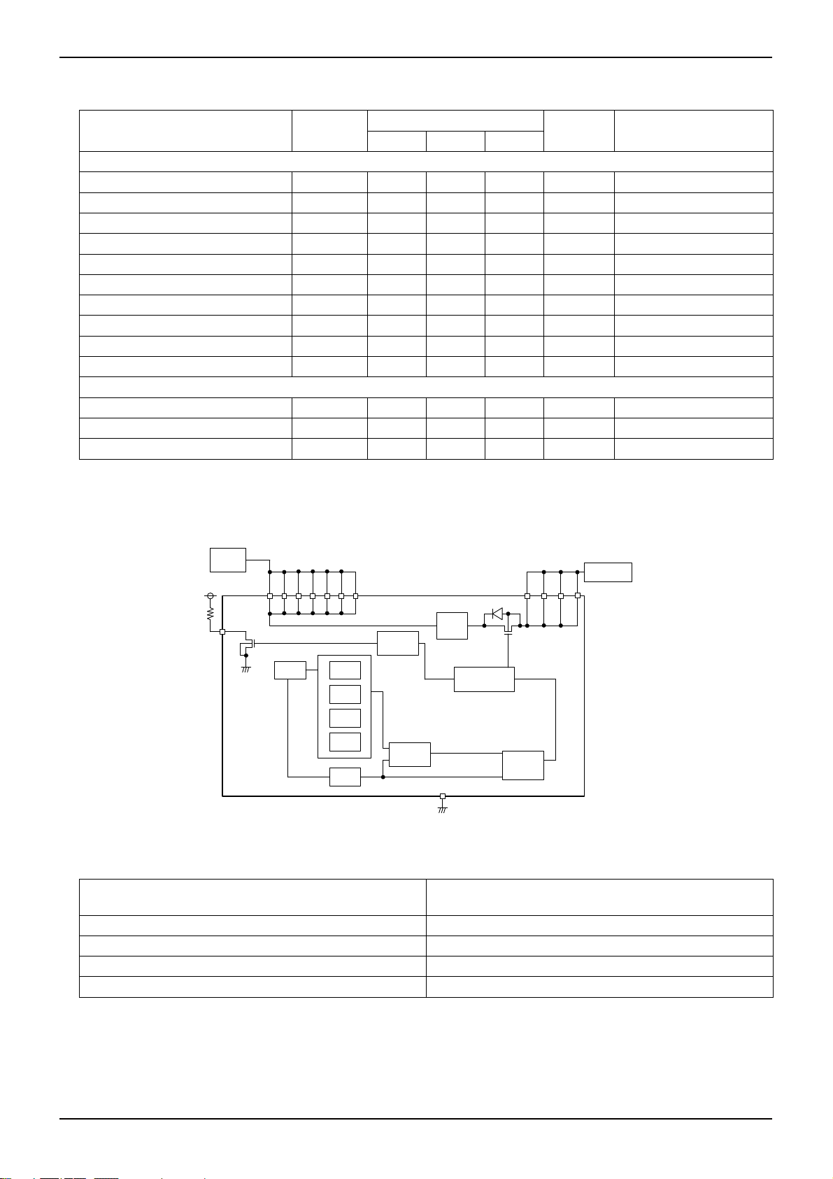
●Block Diagram
Travel
Adapter
IN
IN
IN
IN IN IN IN
OUT
OUT
OUT
CHARGER
OUT
FLGB
●PIN number / PIN name
A3, A4,B3, B4,C4, D3,D4 IN
NVP
GND
Gate
Driver
Initial
Delay
VREF
UVLO
OVLO
OCP
TSD
OSC
Initial
Delay
Timing
Generator
Fig. 1 Block Diagram
Pin number Pin name
A1, B1,C1, D1 OUT
D2 GND
A2 FLGB
www.rohm.com
© 2009 ROHM Co., Ltd. All rights reserved.
2/7
2009.05 - Rev.A
BD6046GUL
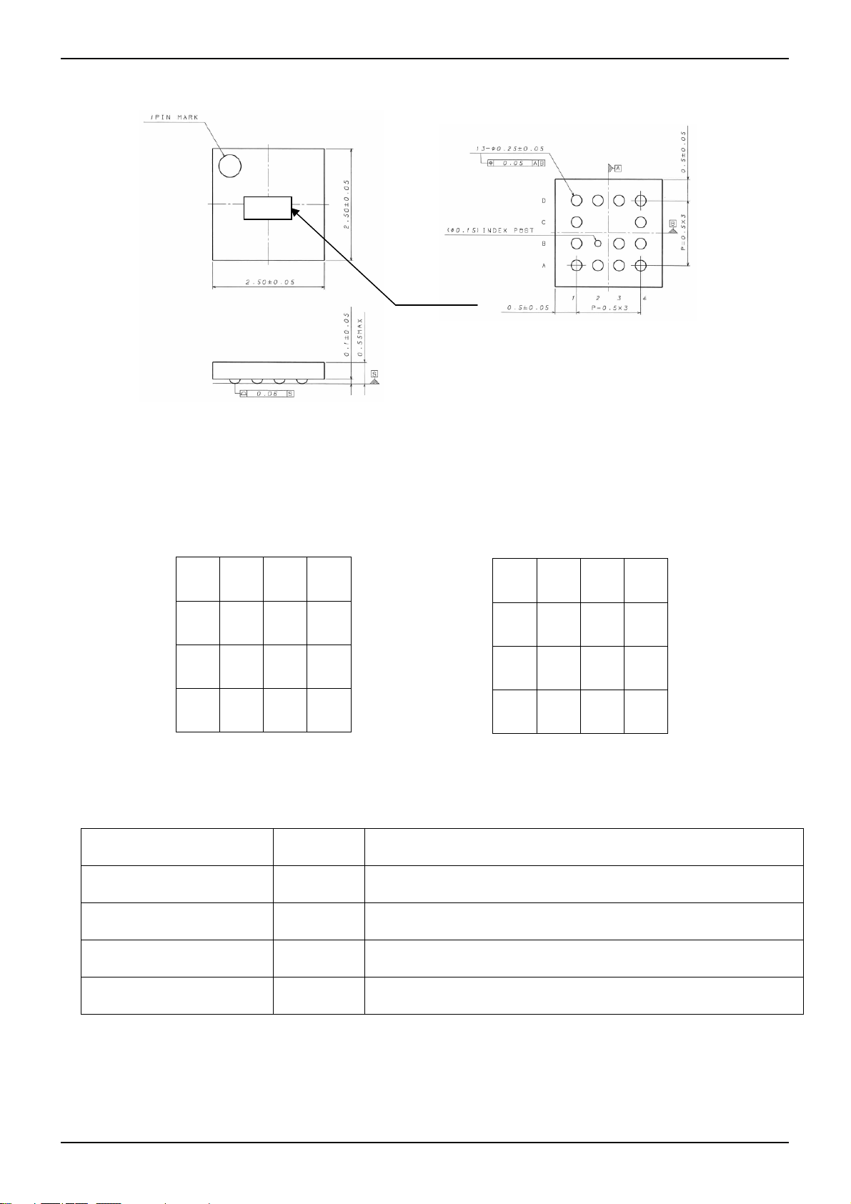
A
A
● Package Dimensions
●Ball Configuration
●PIN DESCRIPTIONS
OUT
OUT
B
C
OUT
OUT
D
1 2 3
BD6046
Top View
FLGB
index
GND
IN
IN
IN
Lot No.
Fig. 2 Package Dimensions (VCSP50L2)
Bottom View
IN
IN
IN
IN
4
Fig. 3 Ball Configuration
D
OUT
C
OUT
B
OUT
OUT
123
GND
index
FLGB
IN
IN
IN
Technical Note
IN
IN
IN
IN
4
PIN NAME FUNCTION
A3, A4, B3, B4, C4, D3, D4 IN
A1, B1, C1, D1 OUT Output Voltage Pin
A2 FLGB
D2 GND Ground Pin
www.rohm.com
© 2009 ROHM Co., Ltd. All rights reserved.
Input voltage Pin. A 1・F low ESR capacitor,
or larger must be connected between this pin and GND
Open-drain output pin that turns low when any protection event occurs.
(overvoltage protection, thermal shut down)
3/7
2009.05 - Rev.A
BD6046GUL
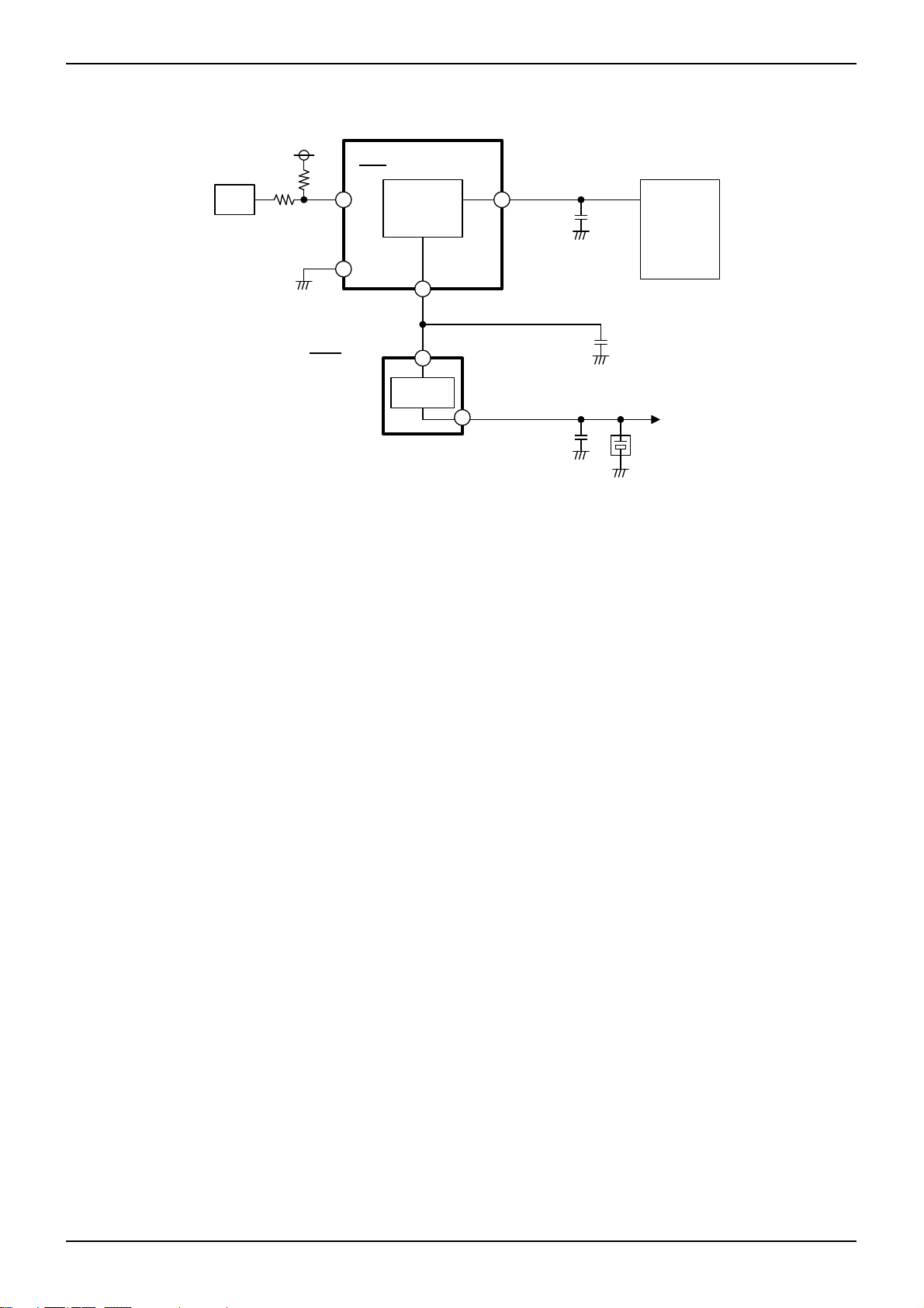
●Typical Application Circuit
Technical Note
OVP
CPU
FLGB
GND
PMIC
28V-OVP
OUT
CHGIN
IN
Charger
BATT
Fig. 4 Application Circuit
・Safety is high because it detects, and it protects it for an abnormal voltage up to 28V.
・It contributes to the miniaturization because all external is built into.
Cin
1.0uF
Travel
Adapter
Cout
4.7uF
Li-ion
1cell
www.rohm.com
© 2009 ROHM Co., Ltd. All rights reserved.
4/7
2009.05 - Rev.A

BD6046GUL
c
●Timing Diagram
Technical Note
OVLO
IN
OUT
FLGB
OUT
FLGB
Fig. 5 Start up sequence
IN
2.0μ sec
(Toff)
1.5μ se
(Tovp)
Fig. 6 Shutdown by over voltage detection
15V
UVLO
2.5msec
(Ton)
OVLO
UVLO
IN
OUT
FLGB
5V
2.5msec
1μ sec
Fig. 7 Recovery from overvoltage protection
www.rohm.com
© 2009 ROHM Co., Ltd. All rights reserved.
5/7
2009.05 - Rev.A

BD6046GUL
●Notes foer use
(1) Absolute maximum ratings
If applied voltage (VDD, VIN), operating temperature range (Topr), or other absolute maximum ratings are exceeded, there
is a risk of damage. Since it is not possible to identify short, open, or other damage modes, if special modes in which
absolute maximum ratings are exceeded are assumed, consider applying fuses or other physical safety measures.
(2) Recommended operating range
This is the range within which it is possible to obtain roughly the expected characteristics. For electrical characteristics, it
is those that are guaranteed under the conditions for each parameter. Even when these are within the recommended
operating range, voltage and temperature characteristics are indicated.
(3) Reverse connection of power supply connector
There is a risk of damaging the LSI by reverse connection of the power supply connector. For protection from reverse
connection, take measures such as externally placing a diode between the power supply and the power supply pin of the LSI.
(4) Power supply lines
In the design of the board pattern, make power supply and GND line wiring low impedance.
When doing so, although the digital power supply and analog power supply are the same potential, separate the digital
power supply pattern and analog power supply pattern to deter digital noise from entering the analog power supply due to
the common impedance of the wiring patterns. Similarly take pattern design into account for GND lines as well.
Furthermore, for all power supply pins of the LSI, in conjunction with inserting capacitors between power supply and GND
pins, when using electrolytic capacitors, determine constants upon adequately confirming that capacitance loss occurring
at low temperatures is not a problem for various characteristics of the capacitors used.
(5) GND voltage
Make the potential of a GND pin such that it will be the lowest potential even if operating below that. In addition, confirm
that there are no pins for which the potential becomes less than a GND by actually including transition phenomena.
(6) Shorts between pins and misinstallation
When installing in the set board, pay adequate attention to orientation and placement discrepancies of the LSI. If it is
installed erroneously, there is a risk of LSI damage. There also is a risk of damage if it is shorted by a foreign substance
getting between pins or between a pin and a power supply or GND.
(7) Operation in strong magnetic fields
Be careful when using the LSI in a strong magnetic field, since it may malfunction.
(8) nspection in set board
When inspecting the LSI in the set board, since there is a risk of stress to the LSI when capacitors are connected to low
impedance LSI pins, be sure to discharge for each process. Moreover, when getting it on and off of a jig in the inspection
process, always connect it after turning off the power supply, perform the inspection, and remove it after turning off the
power supply. Furthermore, as countermeasures against static electricity, use grounding in the assembly process and
take appropriate care in transport and storage.
(9) Input pins
Parasitic elements inevitably are formed on an LSI structure due to potential relationships. Because parasitic elements
operate, they give rise to interference with circuit operation and may be the cause of malfunctions as well as damage.
Accordingly, take care not to apply a lower voltage than GND to an input pin or use the LSI in other ways such that
parasitic elements operate. Moreover, do not apply a voltage to an input pin when the power supply voltage is not being
applied to the LSI. Furthermore, when the power supply voltage is being applied, make each input pin a voltage less than
the power supply voltage as well as within the guaranteed values of electrical characteristics.
(10) Ground wiring pattern
When there is a small signal GND and a large current GND, it is recommended that you separate the large current GND
pattern and small signal GND pattern and provide single point grounding at the reference point of the set so that voltage
variation due to resistance components of the pattern wiring and large currents do not cause the small signal GND voltage
to change. Take care that the GND wiring pattern of externally attached components also does not change.
(11) Externally attached capacitors
When using ceramic capacitors for externally attached capacitors, determine constants upon taking into account a
lowering of the rated capacitance due to DC bias and capacitance change due to factors such as temperature.
(12) Thermal shutdown circuit (TSD)
When the junction temperature reaches the defined value, the thermal shutdown circuit operates and turns a switch OFF.
The thermal shutdown circuit, which is aimed at isolating the LSI from thermal runaway as much as possible, is not aimed
at the protection or guarantee of the LSI.
LSI assuming its operation.
(13) Thermal design
Perform thermal design in which there are adequate margins by taking into account the permissible dissipation (Pd) in
actual states of use.
Therefore, do not continuously use the LSI with this circuit operating or use the
Technical Note
www.rohm.com
© 2009 ROHM Co., Ltd. All rights reserved.
6/7
2009.05 - Rev.A

BD6046GUL
●Ordering part number
B D 6 0 4 6 G U L - E 2
Part No. Part No.
VCSP50L2
1PIN MARK
2.50±0.05
BD6046
(BD6046GUL)
13-φ0.25±0.05
0.05
(φ0.15)INDEX POST
2.50±0.05
0.5±0.05
0.1±0.05
0.06 S
BA
0.55MAX
S
A
D
C
B
A
3
2
1
P=0.5×3
0.5±0.05
B
P=0.5×3
4
(Unit : mm)
Package
GUL : VCSP50L2
<Tape and Reel information>
Embossed carrier tapeTape
Quantity
Direction
of feed
3000pcs
E2
The direction is the 1pin of product is at the upper left when you hold
()
reel on the left hand and you pull out the tape on the right hand
Reel
Technical Note
Packaging and forming specification
E2: Embossed tape and reel
1pin
Order quantity needs to be multiple of the minimum quantity.
∗
Direction of feed
www.rohm.com
© 2009 ROHM Co., Ltd. All rights reserved.
7/7
2009.05 - Rev.A

Notes
No copying or reproduction of this document, in part or in whole, is permitted without the
consent of ROHM Co.,Ltd.
The content specied herein is subject to change for improvement without notice.
The content specied herein is for the purpose of introducing ROHM's products (hereinafter
"Products"). If you wish to use any such Product, please be sure to refer to the specications,
which can be obtained from ROHM upon request.
Examples of application circuits, circuit constants and any other information contained herein
illustrate the standard usage and operations of the Products. The peripheral conditions must
be taken into account when designing circuits for mass production.
Great care was taken in ensuring the accuracy of the information specied in this document.
However, should you incur any damage arising from any inaccuracy or misprint of such
information, ROHM shall bear no responsibility for such damage.
The technical information specied herein is intended only to show the typical functions of and
examples of application circuits for the Products. ROHM does not grant you, explicitly or
implicitly, any license to use or exercise intellectual property or other rights held by ROHM and
other par ties. ROHM shall bear no responsibility whatsoever for any dispute arising from the
use of such technical information.
Notice
The Products specied in this document are intended to be used with general-use electronic
equipment or devices (such as audio visual equipment, ofce-automation equipment, communication devices, electronic appliances and amusement devices).
The Products specied in this document are not designed to be radiation tolerant.
While ROHM always makes ef forts to enhance the quality and reliability of its Products, a
Product may fail or malfunction for a variety of reasons.
Please be sure to implement in your equipment using the Products safety measures to guard
against the possibility of physical injury, re or any other damage caused in the event of the
failure of any Product, such as derating, redundancy, re control and fail-safe designs. ROHM
shall bear no responsibility whatsoever for your use of any Product outside of the prescribed
scope or not in accordance with the instruction manual.
The Products are not designed or manufactured to be used with any equipment, device or
system which requires an extremely high level of reliability the failure or malfunction of which
may result in a direct threat to human life or create a risk of human injur y (such as a medical
instrument, transportation equipment, aerospace machinery, nuclear-reactor controller,
fuel-controller or other safety device). ROHM shall bear no responsibility in any way for use of
any of the Products for the above special purposes. If a Product is intended to be used for any
such special purpose, please contact a ROHM sales representative before purchasing.
If you intend to export or ship overseas any Product or technology specied herein that may
be controlled under the Foreign Exchange and the Foreign Trade Law, you will be required to
obtain a license or permit under the Law.
www.rohm.com
© 2009 ROHM Co., Ltd. All rights reserved.
Thank you for your accessing to ROHM product informations.
More detail product informations and catalogs are available, please contact us.
ROHM Customer Support System
http://www.rohm.com/contact/
R0039
A
 Loading...