

Small-sized Class-D Speaker Amplifiers
Analog Input
Stereo Class-D Speaker Amplifier
BD5471MUV
●Description
BD5471MUV is a low voltage drive class-D stereo speaker amplifier that was developed for note-book PC, cellular phone,
mobile audio products and the others. LC filters of speaker outputs are unnecessary, and only 7 external components are
needed for speaker system. Also, 3.3V regulator in BD5471MUV can use power supply for audio-codec. BD5471MUV, that
is high-efficiency, low consumption, is suitable for application by using battery. Shutdown current is 0µA typically. Also,
start-up time is fast from shutdown to active mode. BD5471MUV can use for some applications that change mode between
“shutdown state” and “active state”.
●Features
1) High power 2.3W typ. (VDD=5V, RL=4Ω, THD+N=10%, stereo input)
High power 1.5W typ. (VDD=5V, RL=8Ω, THD+N=10%, stereo input)
2) Gain selectable by the external control (6, 12, 18, 24dB)
3) Pop noise suppression circuitry
4) Standby function (Mute function) [I
5) Protection circuitry (Short protection [Audio, REG], Thermal shutdown, Under voltage lockout)
6) Built-in 3.3V regulator
7) Built-in BEEP detect circuitry
8) Very small package VQFN024V4040
●Applications
Notebook computers,Mobile electronic applications,Mobile phones,PDA etc.
●Absolute Maximum Ratings(Ta=+25℃)
Parameter Symbol Ratings Unit
=0uA]
SD
No.10101EAT03
Power Supply Voltage VDD 7.0 V
0.7 *1 W
Power Dissipation Pd
2.2 *2 W
Storage Temperature Range Tstg -55 ~ +150 ℃
Input Voltage Range *3 Vin -0.3 ~ VDD+0.3 V
Control Terminal
Input Voltage Range *4
*1 74.2mm×74.2mm×1.6mm, FR4 1-layer glass epoxy board(Copper on top layer 0%)
Derating in done at 5.6mW/℃ for operating above Ta=25℃. There are thermal via on the board
*2 4.2mm×74.2mm×1.6mm, FR4 4-layer glass epoxy board (Copper on bottom 2 and 3 layer 100%)
*3 input Terminal (INL+, INL-, INR+, INR-)
*4 Control Terminal (MUTE, G0, G1, EAPD, BEEP, REG_SD)
●Operating Conditions
Parameter Symbol Ratings Unit
Power Supply Voltage
Temperature Range
* These products aren’t designed for protection against radioactive rays.
Vctl -0.3 ~ VDD+0.3 V
VDD +4.5 ~ +5.5 V
Topr -40 ~ +85 ℃
www.rohm.com
© 2010 ROHM Co., Ltd. All rights reserved.
1/21
2010.06 - Rev.A
BD5471MUV
Technical Note
●Electric Characteristics(Unless otherwise specified, Ta=+25℃, VDD=+5.0V, RL=8Ω, AC item= LC Filter(L=22µH, C=1µF) )
Parameter Symbol
Circuit current (Active)
Circuit current (Standby)
Circuit current (Regulator)
Circuit current (Shutdown)
I
I
STBY
I
CCR
I
CC
SD
MIN. TYP. MAX.
Limits
― 5.5 12.0 mA
Unit Conditions
Active mode,
MUTE=H, EAPD=H, No load
― 0.1 1.0 mA Standby mode, MUTE=H,EAPD=L
― 0.15 1.0 mA
― 0.1 2.0 µA
Regulator Mode, MUTE=EAPD=L
REG_SD=H
Shutdown mode, MUTE=L,
REG_SD=L
<Speaker Amplifier>
Output power 1 P
Output power 2 P
0.8 1.2 ― W
O1
1.0 1.5 ― W
O2
BTL, f=1kHz, THD+N=1%,
Stereo input, *1, *2
BTL, f=1kHz, THD+N=10%,
Stereo input, *1, *2
5.5 6.0 6.5 dB BTL, G0=G1=GND
11.5 12 12.5 dB BTL, G0=GND, G1=VDD
Voltage gain GV
17.5 18 18.5 dB BTL, G0=VDD, G1=GND
23.5 24 24.5 dB BTL, G0=G1=VDD
Total harmonic distortion THD+N ― 0.2 1.0 % BTL, Po=0.7*P
Crosstalk C
60 70 ― dB BTL, f=1kHz *1, *3
T
S/N SNR 70 90 ― dB BTL, Po=P
Switching Frequency fosc 175 250 325 kHz
Start-up time Ton 0.78 1.02 1.46 msec
63 90 117 kΩ G0=G1=GND
42 60 78 kΩ G0=GND, G1=VDD
Input resistance R
IN
25 36 47 kΩ G0=VDD, G1=GND
14 20 26 kΩ G0=G1=VDD
<Regulator>
Output voltage Vo 3.15 3.30 3.45 V Io=150mA
Maximum output current Iom 150 200 ― mA Vo=3.15V
Load regulation L
― 0.2 1 mV/mA Io=0→150mA
REG
<Control terminal (MUTE, G0, G1, EAPD, BEEP, REG_SD) >
Control terminal
input voltage
High-level
Low-level
Control terminal input current
*1: B.W.=400 ~ 30kHz, BTL:The voltage between 3pin and 6pin, 13pin and 16pin
V
V
CTLH
CTLL
I
CTL
1.4 ― VDD V
0 ― 0.4 V
22 33 44 µA
Control terminal Input voltage
V
CTL
●Active / Standby Control
Mode Pin level Conditions
MUTE H/L IC active/ shutdown
EAPD H/L IC active/standby
BEEP H/L IC active/standby
REG_SD H/L REG active/shutdown
=5V
O1
*1, *2
O1
*1, *3
www.rohm.com
© 2010 ROHM Co., Ltd. All rights reserved.
2/21
2010.06 - Rev.A
BD5471MUV
A
_
2.2μF
E
S
C11
8
C9
S
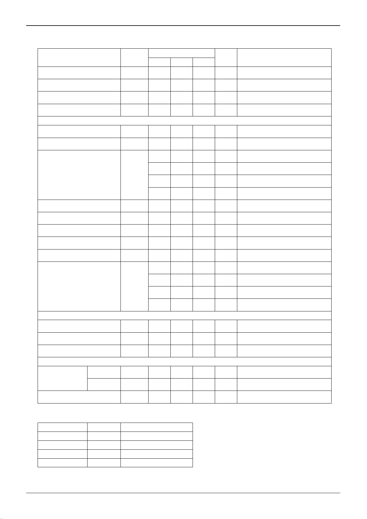
●Measurement Circuit Diagram
V
BEEP
BEEP
A
1
V
V
SE
22μF
1μF
V
V
BTL
8Ω
VDD
DET_C
C1
0.01u
F
OUTL
PVDD
PGNDL
2
3
4
5
V
V
SE
22μF
1μF
OUTL-
6
●Package Outlines
D5471
Vin Vin Vin Vin
C
0.1μF
24 19202122
150k
SHORT
SHORT
SHORT
SHORT
MUT
7 8 9 10 11
A
C7
0.1μF
INL - INR
23
BEEP
DE T
BEEP
H-
Bridge
150k
EAPD
MUTE EAP REG_S
A
V
MUTE
BEEP
MUT
EAPD
150k
V
EAPD
Gain
Select
PWM
GNDINL+
UVLO TSD SHOR
BIAS
A
V
10u
C6
G0
G0
G1 G1
STOP
OSC
REG_
VDD
VDD
AVD D
Gain
Select
PWM
UVLO
T
3.3VRE
REG_VD
C2
+B
D
VQFN024V4040 (Plastic Mold)
UVLO
T
C5
0.1 μF
Bridg
D
REG_OU
C4
0.1μF
INR+
G0
150 k
G1
150k
SHORT
H-
SHORT
REG
12
C3
Bottom View Top View
(Unit: mm)
Technical Note
V
G0
18
G1
17
OUT R
16
PVDD
15
PGND
14
OUTR-
13
GN
G0
A
V
G1
A
22μF
1μF
8Ω
22μF
1μF
V
V
SE
V
BTL
V
V
SE
V
www.rohm.com
© 2010 ROHM Co., Ltd. All rights reserved.
3/21
2010.06 - Rev.A
BD5471MUV
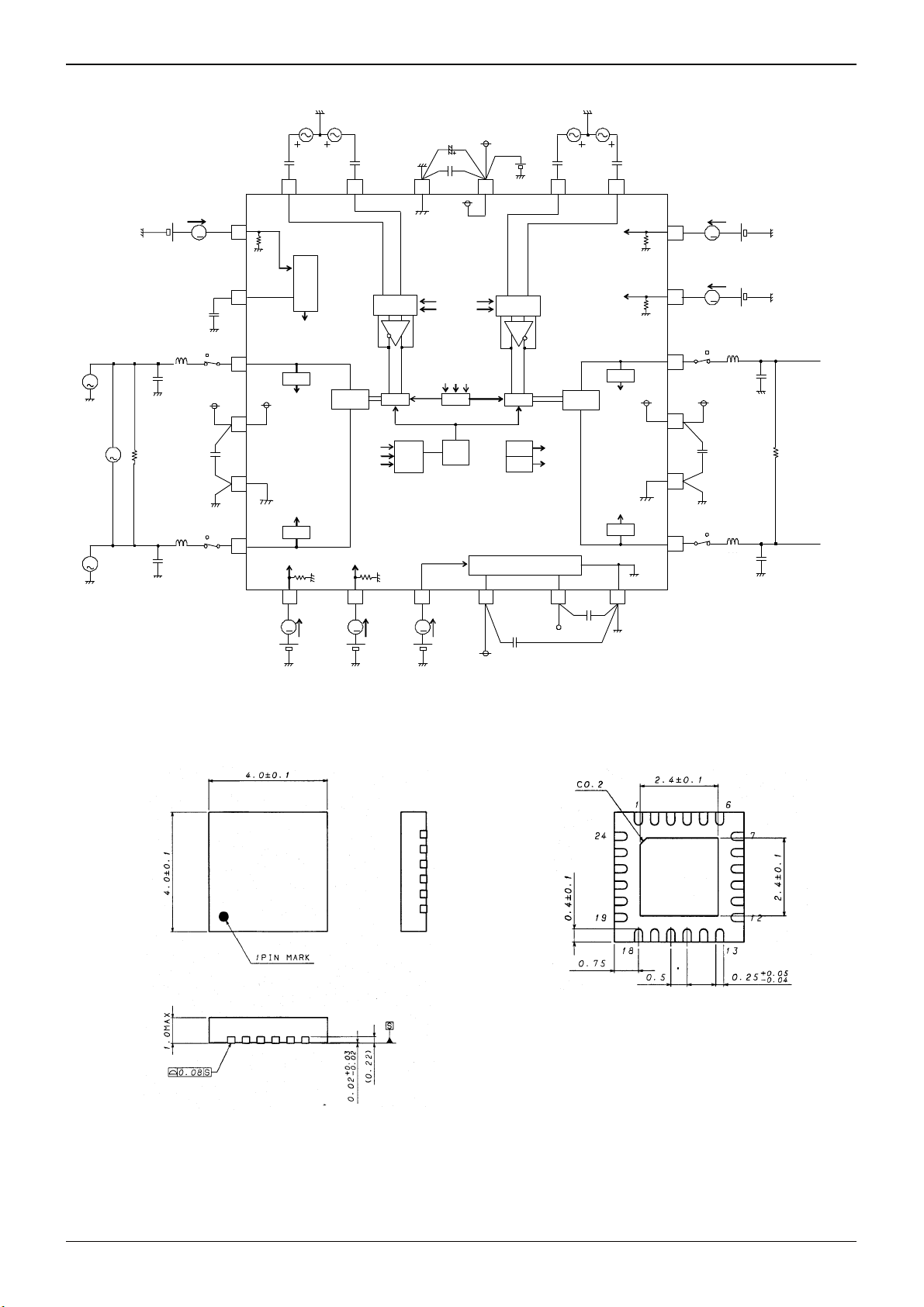
●Block Diagram ●Pin Assignment <top view>
INL+
24
INL-
23
INR+
19
INR-
20
G0
18
G1
17
MUTE
7
EAPD
8
BEEP
1
DET_C
2
REG_SD
9
150k
150k
150k
150k
150k
150k
PVDDL
4
Gain
Select
G0 G1
Gain
Select
G0 G1
G0
G1
REG
12
REG_GND
REG_VDD
10 15
Short
TSD
UVLO
Bias
BEEP
Detect
5
PGNDL
3.3V
PVDDR
PWM
PWM
OSC
14
PGNDR
ERROR
ERROR
Control
Logic
Short
Protection
AVDD
21
HBridge
Short
Protection
HBridge
ERROR
22
AGND
OUTL+
3
6
OUTL-
OUTR+
16
13
OUTR-
REG_OUT
11
24 23 22 21 20 19
INL+
INL-
AGND
BEEP
1
2
DET_C
3
OUTL+
PVDDL
4
5
PGNDL
OUTL-
6
EAPD
MUTE
7 8 9 10 11 12
REG SD
●Pin Assignment Table
PIN No. PIN Name
1 BEEP
2 DET_C
3 OUTL+
4 PVDDL
5 PGNDL
6 OUTL7 MUTE
8 EAPD
9 REG_SD
10 REG_VDD
11 REG_OUT
12 REG_GND
13 OUTR14 PGNDR
15 PVDDR
16 OUTR+
17 G1
18 G0
19 INR+
20 INR21 AVDD
22 AGND
23 INL24 INL+
Technical Note
INR-
AVDD
REG VDD
INR+
G0
18
17
G1
OUTR+
PVDDR
PGNDR
OUTR-
REG OUT
REG GND
16
15
14
13
www.rohm.com
© 2010 ROHM Co., Ltd. All rights reserved.
4/21
2010.06 - Rev.A
BD5471MUV
●Application Circuit Example
Differential
Input
Differential
Input
Gain
Control
BEEP
H:Active
L:Shutdown
MUTE
EAPD
REG_SD
Audio
InputL+
Audio
InputL-
Audio
InputR+
Audio
InputR-
G0
G1
0.01μF
0.1μF
C2
0.1μF
C1
0.1μF
C4
0.1μF
C3
C8
REG_SD
INL+
INL-
INR+
INR-
MUTE
EAPD
BEEP
DET_C
Technical Note
C5
10μF
PVDDL
REG_VDD
10 15
4
24
Gain
Select
23
G0 G1
19
Gain
Select
20
G0 G1
G0
18
G1
17
7
8
1
2
9
150k
150k
150k
150k
150k
150k
REG_GND
REG
G0
G1
12
PGNDL
Bias
BEEP
Detect
Short
TSD
UVLO
5
PWM
PWM
OSC
3.3V
14
PVDDR
Short
Control
Logic
Short
Protection
PGNDR
21
HBridge
ERROR
HBridge
ERROR
22
AVDD
Short
Protection
ERROR
AGND
OUTL+
3
6
OUTL-
OUTR+
16
13
OUTR-
REG_OUT
11
2.2μF
C7
Sing le-Ended
Input
Sing le-Ended
Input
Gain
Contr ol
BEEP
H:Active
L:Shutdown
MUTE
EAPD
REG _SD
Audio
Input L
Audio
Input R
G0
G1
0.01μF
Differential input
C5
10μF
PVDDL
REG_VDD
4
Gain
Sele ct
Gain
Sele ct
G0
G1
REG
12
Bias
BEEP
Detect
PGNDL
10 15
PWM
PWM
Short
TSD
UVLO
OSC
3.3V
5
14
0.1μF
INL+
24
C2
INL-
0.1μF
0.1μF
C4
0.1μF
DET_C
C8
REG_SD
INR+
INR-
G0
G1
MUTE
EAPD
BEEP
23
G0 G1
19
20
G0 G1
18
150k
17
150k
7
150k
8
150k
1
150k
2
9
150k
REG_GND
C1
C3
PVDDR
Short
Cont rol
Logic
Short
Protection
PGND R
21
HBridge
ERROR
Shor t
Protection
HBridge
ERROR
22
AGND
AVDD
ERROR
OUTL+
3
6
OUTL-
OUTR+
16
13
OUTR-
REG_OUT
11
2.2μF
C7
www.rohm.com
© 2010 ROHM Co., Ltd. All rights reserved.
Single-Ended input
5/21
2010.06 - Rev.A
BD5471MUV
●Evaluation board Circuit Diagram
JP1
BEEP
1
DET_C
C1
2
OUTL+
3
to Speaker
(BTL)
PVDDL
PGNDL
4
5
OUTL-
6
Please connect
to Input Signal line.
Please connect
to Power Supply
(VDD=+2.5~5.5V) line.
Please connect
to GND line.
Audio Input
C7 C6
INL+ INL-
23
24
150k
BEEP
DET
BEEP
SHORT
H-
SHORT
SHORT
SHORT
MUTE
7
Bridge
BEEP
MUTE
EAPD
EAPD
150k
150k
MUTE
8
JP2 JP3 JP4
AGND
22
Gain
G0
Select
G1 G1
UVLO
PWM
STOP
BIAS
EAPD RE G_SD
9
C5
C8
TSD SHORT
OSC
Technical Note
Audio Input
C4 C3
Gain
Select
PWM
UVLO
TSD
3.3VREG
UVLO
20
TSD
11
INR-
H-
Bridge
REG_OUT
C2
19
G0
G1
SHORT
SHORT
12
INR+
150k
150k
REG_GND
G0
18
G1
17
OUTR+
16
PVDDR
15
PGNDR
14
OUTR-
13
JP4
JP5
to Speaker
(BTL)
Please connect
to Speaker.
AVDD
21
G0
REG_VDD
10
3.3V
Regulator
www.rohm.com
© 2010 ROHM Co., Ltd. All rights reserved.
6/21
2010.06 - Rev.A
BD5471MUV
●Evaluation board Parts List
Qty. Item Description SMD Size Manufacturer/Part Number
Technical Note
1 C1 Capacitor, 0.01μF 1608
1 C2 Capacitor, 2.2μF 1608
2 C3, C4,C6,C7 Capacitor, 0.1μF 1608
1 C5, C8 Capacitor, 10μF A (3216)
1 U1
1 PCB1
●The relation in the gain setting and input impedance Ri
The gain setting terminal (G0,G1)
G0 G1 Gain[dB] Ri [Ohm]
L L 6 90k
L H 12 60k
H L 18 36k
H H 24 20k
●Description of External parts
①Power down timing capacitor (C1)
It’s the capacitor which adjusts time from BEEP signal stop to amplifier stop.
Turn off time Toff is set the following formula.
Toff
②Regulator output capacitor(C2)
Output capacitor of 3.3V regulator.
Use capacitance equal to or more than 1uF.
③Input coupling capacitor Ci (C3,C4, C6,C7)
It makes an Input coupling capacitor 0.1uF.
Input impedance Ri in each gain setting becomes the above table.
In 18dB gain setting, it is Ri=36kΩ(Typ.).
It sets cutoff frequency fc by the following formula by input coupling capacitor Ci (C3,C4, C6,C7) and input impedance Ri
fc
In case of Ri=36kΩ, Ci=0.1uF, it becomes fc=about 44Hz.
④The power decoupling capacitor (C5,C8)
It makes a power decoupling capacitor 10uF.
When making capacitance of the power decoupling capacitor small, there is an influence in the Audio characteristic.
When making small, careful for the Audio characteristic at the actual application.
8.0
VDDC1
[ms]
μ
5
1
[Hz]
CiRi2π
IC, BD5471MUV,
Stereo Class-D audio
amplifier
Printed-circuit board,
BD5471MUV EVM
4.0mm X 4.0mm
VQFN Package
― ―
Murata
GRM188R71C103KA01D
Murata
GRM188R61C225KE15D
Murata
GRM188R71C104KA01D
ROHM
TCFGA1A106M8R
ROHM
BD5471MUV
www.rohm.com
© 2010 ROHM Co., Ltd. All rights reserved.
7/21
2010.06 - Rev.A

BD5471MUV
●Evaluation board PCB layer
Technical Note
Top Layer
Bottom Layer
www.rohm.com
© 2010 ROHM Co., Ltd. All rights reserved.
8/21
2010.06 - Rev.A

BD5471MUV
5
Technical Note
●The way of evaluating Audio characteristics
Evaluation Circuit Diagram
3.3 V
PWM
PWM
OSC
14
C5
10μF
PVDDR
Short
Control
Logic
Short
Protection
PGNDR
AV DD
21
HBridge
ERROR
Short
Pr otect ion
HBridge
ERROR
22
AGND
ERROR
OUT L+
3
6
OUT L-
OUT R
16
13
OUT R-
REG_OUT
11
C7
22μF
22μF
22μF
22μF
2.2μF
1μF
R
1μF
RL=Speaker Load
1μF
R
1μF
RL=Speaker Load
Me asur eme nt In stru men t
Audio
Precision
L
BTL
Me asur eme nt In stru men t
Audio
BTL
Precision
L
etc.
etc.
PVDDL
Gain
Control
BEEP
Audio
InputL+
Audio
InpuLt-
Audio
Input R+
Audio
Input R-
G0
G1
MUTE
EAPD
0.01μF
0.1μF
C2
0.1μF
C1
0.1μF
C4
0.1μF
C3
C8
INL+
24
INL-
23
INR +
19
INR-
20
G0
18 G0
G1
17
MUTE
7
EAPD
8
BEEP
1
DET_C
2
150k
150k
150k
150k
150k
Di ffer ent ial
Input
Di ffer ent ial
Input
REG_VDD
4
Gai n
Select
G0 G1
Gai n
Select
G0 G1
G1
10 15
Short
TSD
UVL
Bias
BEEP
Detect
H:Active
L:Shutdown
REG_SD
RE G_S
9
150k
REG_GND
REG
12
PGNDL
When measuring Audio characteristics, insert LC filter during the output terminal of IC and the speaker load and measure it.
it. Arrange LC filter as close as possible to the output terminal of IC.
In case of L=22μH, C=1μF, the cutoff frequency becomes the following.
fcπ2
1
[Hz]
LC
=33.9[kHz]
Use a big current type - Inductor L.
(Reference)
TDK: SLF12575T-220M4R0
www.rohm.com
© 2010 ROHM Co., Ltd. All rights reserved.
9/21
2010.06 - Rev.A

BD5471MUV
●BEEP Detection Function
This IC has BEEP detection.
When inputting beep signal to 1pin BEEP terminal at standby mode, amplifier becomes standby to active.
When beep signal stops, amplifier becomes active to standby.
It is adjustable the time(Toff) from beep signal stop to amplifier standby by a capacitance connect to 2pin DET_C terminal.
If no need to use BEEP detection, make 1pin BEEP terminal open or connect to GND.
MUTE
BEEP
DET_C
Amplifier
state
Toff calculation fomula
To ff =
C×0.8VDD
5u
Example C=0.01u, VDD=5V → Toff= 8 mse c
C: Condenser to connect to a 2pin
MUTE=H, BEEP signal input MUTE=H, BEEP signal stop
Ton
[msec]
Active
Active
VDD
0.2×VDD
Active
Standby
To ff
DET_C 2V/div
OUTL+ 5V/div
BEEP 5V/div
To ff
Technical Note
www.rohm.com
© 2010 ROHM Co., Ltd. All rights reserved.
10/21
2010.06 - Rev.A

BD5471MUV
●Cntrol Terminal and output
Audio IN
[ Input ]
EAPD
[ Input ]
BEEP
[ Input ]
MUTE
[ Input ]
Amplifier state
Standby Standby Standby Shutdown
Speaker output
MUTE EAPD BEEP Audio IN Amplifier state Speaker output
L L L No signal L(Shutdown) Hiz
L L L signal L(Shutdown) Hiz
L L H No signal L(Shutdown) Hiz
L L H signal L(Shutdown) Hiz
L H L No signal L(Shutdown) Hiz
L H L signal L(Shutdown) Hiz
L H H No signal L(Shutdown) Hiz
L H H signal L(Shutdown) Hiz
H L L No signal L(Standby) Hiz
H L L signal L(Standby) Hiz
H L H No signal H(Active) No signal
H L H signal H(Active) signal
H H L No signal H(Active) No signal
H H L signal H(Active) signal
H H H No signal H(Active) No signal
H H H signal H(Active) signal
Technical Note
Audio Signal Beep Signal Audio Signal Beep Signal Audio Signal
In case of EAPD=L,
it doesn’t output.
Beep Signal
Equal to or more than
0.125sec.
It detects that
BEEP was inputted.
Amplifier is a standby.
The current consumption reduces.
It makes an amplifier state to
standby mode if BEEP isn’t
inputted equal to or more than 3.3msec.
Active Active
Input Output
f=300~1760Hz
3.3msec 570usec
The current consumption
in the audio part is zero.
www.rohm.com
© 2010 ROHM Co., Ltd. All rights reserved.
11/21
2010.06 - Rev.A

BD5471MUV
●About output starting and stop
This IC has the cuircuit of pop noise reduction at starting and stop.
Pop noise reduction is realized in controlling to adjust the timing of output at starting and stop.
Turn on time is 1msec.
●About the short protection
Output starting (MUTE=H, EAPD=L→H)
Ton=1msec
H-
Bridge
Short
Protection
Short
Protection
H-
Bridge
OUTL+
OUTL-
OUTR+
OUTR-
Output stop (MUTE=H, EAPD=H→L)
EAPD
5V/div
OUTL+
5V/div
OUTL5V/div
When detecting a short of Lch output,
Lch output stops, and Rch output stops.
Also when detecting a short of Rch output,
Rch output stops, and Lch output stops.
Technical Note
www.rohm.com
© 2010 ROHM Co., Ltd. All rights reserved.
12/21
2010.06 - Rev.A

BD5471MUV
Technical Note
●About the thermal design by the IC
Characteristics of an IC have a great deal to do with the temperature at which it is used, and exceeding absolute maximum
ratings may degrade and destroy elements. Careful consideration must be given to the heat of the IC from the two
standpoints of immediate damage and long-term reliability of operation. Pay attention to points such as the following.
Since an maximum junction temperature (Tj
.)or operating temperature range (Topr) is shown in the absolute maximum
MAX
ratings of the IC, to reference the value, find it using the Pd-Ta characteristic (temperature derating curve).
If an input signal is too great when there is insufficient radiation, TSD (thermal shutdown) may operate. TSD, which
operates at a chip temperature of approximately +180℃, is canceled when this goes below approximately +100℃.
Since TSD operates persistently with the purpose of preventing chip damage, be aware that long-term use in the vicinity
that TSD affects decrease IC reliability.
Temperature Derating Curve
Reference Data
3.5
③3.1W
3.1
VQFN024V4040
measurement conditions
: IC unit Rohm standard board mounted
board size : 74.2mm×74.2mm×1.6mmt
board① FR4 1-layer glass epoxy board(Copper on top layer 0%)
board② FR4 4-layer glass epoxy board(Copper on 2,3 layer 100%)
board size : 35mm×25mm×1.6mmt
board③ FR4 4-layer glass epoxy board(Copper on 2,3 layer 100%)
connecting with thermal via
2.5
②2.2W
2.2
2.0
1.5
Power dissipation Pd(W)
1.0
①0.7W
0.7
0.5
0.0
0 25 50 75 100 125
85
Ambient temperature Ta(℃)
150
Note) Values are actual measurements and are not guaranteed.
Power dissipation values vary according to the board on which the IC is mounted. The Power dissipation of this IC when
mounted on a multilayer board designed to radiate is greater than the values in the graph above.
www.rohm.com
© 2010 ROHM Co., Ltd. All rights reserved.
13/21
2010.06 - Rev.A

BD5471MUV
●Typical Characteristics
TABLE OF GRAPHS
Efficiency vs Output power 1, 2
Power dissipation vs Output power 3, 4
Supply current (Iccact) vs Supply voltage 5
Supply current (Istby) vs Supply voltage 6
Supply current (Ireg) vs Supply voltage 7
Shutdown current (Isd) vs Supply voltage 8
Parameter Parameter Figure
Technical Note
Output power (Po)
Total harmonic distortion plus noise (THD+N)
Supply voltage rejection ratio (PSRR) vs Frequency 25, 26, 27, 28
Common-mode rejection ratio (CMRR) vs Frequency 29, 30
Gain vs Frequency 31, 32, 33, 34, 35, 36, 37, 38
vs Load resistance 9, 10
vs Supply voltage 11, 12
vs Output power 13, 14
vs Frequency 15, 16, 17, 18, 19, 20, 21,22
vs Common-mode input voltage 23, 24
www.rohm.com
© 2010 ROHM Co., Ltd. All rights reserved.
14/21
2010.06 - Rev.A

BD5471MUV
Technical Note
100
90
80
70
60
50
40
Efficiency [%]
30
20
10
0
0 0.1 0.2 0.3 0.4 0.5 0.6 0.7 0.8 0.9 1 1.1 1.2
350
300
250
200
150
Icc [mA]
100
50
0
0 0.1 0.2 0.3 0.4 0 .5 0.6 0.7 0.8 0.9 1 1 .1 1.2
6
Efficiency - Output power
f=1kHz RL=8Ω+33uH LC-filter(22uH+1uF)
VDD=2.5V
VDD=3.6V
VDD=5.0V
Po [W]
Fig.1
Ic c vs Ou tput powe r
f=1kHz RL=8Ω+33uH LC-filter(22uH+1uF)
VDD=2.5V
VDD=3.6V
VDD=5.0V
Po [W]
Fig.3
Ic c - V DD
No load, No signal
90
80
70
60
50
40
Efficiency [%]
30
20
10
0
0 0.2 0.4 0.6 0.8 1 1.2 1.4 1.6 1.8 2
600
500
400
300
Icc [mA]
200
100
0
0 0.2 0.4 0.6 0.8 1 1.2 1.4 1.6 1.8 2
0.3
Efficiency vs Output power
f=1kHz RL=4Ω+33uH LC-filter(22uH+1uF)
VDD=2.5V
VDD=3.6V
VDD=5.0V
Po [W]
Fig.2
Icc vs Output power
f=1kHz RL=4Ω+33uH LC-filter(22uH+1uF)
VDD=2.5V
VDD=3.6V
VDD=5.0V
Po [W]
Fig.4
Ic cstby - VDD
No load, No signal
5
0.25
4
3
Icc [mA]
2
1
0
0123456
VDD [V]
Fig.5 Fig.6
Iccreg - VDD
No load, No signal
0.3
0.2
0.15
Iccstby [mA]
0.1
0.05
0
0123456
0.5
VDD [V]
Iccsd - VDD
0.25
0.2
0.15
Iccreg [mA]
0.1
0.05
0
0123456
VDD [V]
Fig.7
www.rohm.com
© 2010 ROHM Co., Ltd. All rights reserved.
15/21
0.4
0.3
Isd [uA]
0.2
0.1
0
0123456
VDD [V]
Fig.8
2010.06 - Rev.A

BD5471MUV
Technical Note
3.0
2.5
2.0
1.5
Po[W]
1.0
0.5
0.0
3.0
2.5
2.0
1.5
Po [W]
1.0
0.5
0.0
10
Output power vs RL THD+N=10%
f=1kHz LC-filter(22uH+1uF) 400Hz-30kHz
VDD=2.5V
VDD=3.6V
VDD=5.0V
4 8 12 16 20 24 28 32
RL[Ω]
Fig.9 Fig.10
f=1kHz LC-filter(22uH+1uF) 400Hz-30kHz
4.5 4.7 4.9 5.1 5.3 5.5
Output power vs VDD
RL=8Ω:THD+N=1%
RL=8Ω:THD+N=10%
VDD [V]
Fig.11 Fig.12
THD+ N vs O u tpu t powe r RL=8Ω
f=1kHz LC-filter(22uH+1uF) 400Hz-30kHz
2.5
2.0
1.5
Po[W]
1.0
0.5
0.0
4.0
3.5
3.0
2.5
2.0
Po [W]
1.5
1.0
0.5
0.0
4.54.74.95.15.35.5
10
Output power vs RL THD+N=1%
f=1kHz LC-filter(22uH+1uF) 400Hz-30kHz
VDD=2.5V
VDD=3.6V
VDD=5.0V
4 8 12 16 20 24 28 32
RL[Ω]
Output power vs VDD
f=1kHz LC-filter(22uH+1uF) 400Hz-30kHz
RL=4Ω:THD+N=1%
RL=4Ω:THD+N=10%
VDD [V]
THD+ N vs O u tpu t powe r RL=4Ω
f=1kHz LC-filter(22uH+1uF) 400Hz-30kHz
1
THD+N [%]
VDD=4.5V
VDD=5.0V
VDD=5.5V
1
THD+N [%]
VDD=4.5V
VDD=5.0V
VDD=5.5V
0.1
0.01 0.1 1 10
Po [W]
Fig.13
THD+N vs Frequency VDD=5.5V RL=8Ω
10
1
LC-filter(22uH+1uF) 30kHz-LPF
Po=50mW
Po=250mW
Po=1W
0.1
0.01 0.1 1 10
Po [W]
Fig.14
THD+N vs Frequency VDD=5.5V RL=4Ω
10
1
LC-filter(22uH+1uF) 30kHz-LPF
Po=50mW
Po=250mW
Po=1W
THD+N [%]
0.1
0.01
10 100 1k 10k 100k
fre q [ Hz]
Fig.15 Fig.16
www.rohm.com
© 2010 ROHM Co., Ltd. All rights reserved.
16/21
THD+N [%]
0.1
0.01
10 100 1k 10k 100k
fre q [ Hz]
2010.06 - Rev.A

BD5471MUV
Technical Note
10
1
THD+N vs Frequency VDD=5.0V RL=8Ω
LC-filter(22uH+1uF) 30kHz-LPF
Po=50mW
Po=250mW
Po=1W
THD+N vs Frequency VDD=5.0V RL=4Ω
10
1
LC-filter(22uH+1uF) 30kHz-LPF
Po=50mW
Po=250mW
Po=1W
THD+N [%]
0.1
THD+N [%]
0.1
0.01
10 100 1k 10k 100k
fre q [Hz ]
Fig.17
THD+N vs Frequency VDD=4.5V RL=8Ω
10
1
LC-filter(22uH+1uF) 30kHz-LPF
Po=50mW
Po=250mW
Po=500mW
0.01
10 100 1k 10k 100k
fre q [Hz ]
Fig.18
THD+N vs Frequency VDD=4.5V RL=4Ω
LC-filter(22uH+1uF) 30kHz-LPF
10
Po=50mW
Po=250mW
Po=500mW
1
THD+N [%]
0.1
THD+N [%]
0.1
0.01
10 100 1k 10k 100k
fre q [Hz]
Fig.19
THD+N vs Frequency RL=8Ω Po=125mW
10
1
LC-filter(22uH+1uF) 30kHz-LPF
VDD=4.5V
VDD=5.0V
VDD=5.5V
0.01
10 100 1k 10k 100k
fre q [Hz]
Fig.20
THD+N vs Fr equ e ncy RL=4Ω Po=250mW
10
1
LC-filter(22uH+1uF) 30kHz-LPF
VDD=4 .5V
VDD=5 .0V
VDD=5 .5V
THD+N [%]
0.1
0.1
THD+N [%]
0.01
10 100 1k 10k 100k
fre q [Hz]
Fig.21 Fig.22
THD+N_vs_Common Mode Input Voltage f=1kHz
RL=8Ω Po=100mW LC-filter(22uH+1uF) 400Hz-30kHz
2.0
VDD=4 .5V
1.5
VDD=5 .0V
VDD=5 .5V
0.01
10 100 1k 10k 100k
THD+N_vs_Common Mode Input Voltage f=1kHz
RL=4Ω Po=200mW LC-filter(22uH+1uF) 400Hz-30kHz
2.0
VDD=4 .5V
1.5
VDD=5 .0V
VDD=5 .5V
fre q [Hz ]
1.0
THD+N [%]
0.5
0.0
01234567
Vic - Common Mode Input Voltage [V]
Fig.23 Fig.24
www.rohm.com
© 2010 ROHM Co., Ltd. All rights reserved.
17/21
1.0
THD+N [%]
0.5
0.0
012345 67
Vic - Common Mode Input Voltage [V]
2010.06 - Rev.A

BD5471MUV
Technical Note
PSRR [dB]
PSRR RL=8Ω Vripple=0.1Vpp Inputs ac-Grounded
Cin=1uF LC-filter(22uH+1uF) 30kHz-LPF
VDD=4.5V
VDD=5.0V
VDD=5.5V
10 100 1k 10k 100k
f [Hz]
PSRR [dB]
0
-10
-20
-30
-40
-50
-60
-70
-80
Fig.25
PSRR RL=8Ω Vripple=0.1Vpp Inputs Floating
0
-10
-20
-30
-40
-50
-60
-70
-80
10 100 1k 10k 100k
LC-filter(22uH+1uF) 30kHz-LPF
VDD=4.5V
VDD=5.0V
VDD=5.5V
f [Hz]
Fig.27 Fig.28
CMRR RL=8Ω Vin=1Vpp Cin=1uF
-40
-45
-50
-55
CMRR [dB]
-60
LC-filter(22uH+1uF) 30kHz-LPF
VDD=4.5V
VDD=5.0V
VDD=5.5V
PSRR RL=4Ω Vripple=0.1Vpp Inputs ac-Grounded
Cin=1uF LC-filter(22uH+1uF) 30kHz-LPF
0
-10
-20
-30
-40
PSRR [dB]
-50
-60
-70
-80
10 100 1k 10k 100k
VDD=4.5V
VDD=5.0V
VDD=5.5V
f [Hz]
Fig.26
PSRR RL= 4Ω Vripple =0.1V pp I nputs F lo ating
LC-filter(22uH+1uF) 30kHz-LPF
0
-10
-20
-30
-40
PSRR [dB]
-50
-60
-70
-80
10 100 1k 10k 100k
-40
-45
-50
-55
CMRR [dB]
-60
VDD=4.5V
VDD=5.0V
VDD=5.5V
f [Hz]
CMRR RL=4Ω Vin=1Vpp Cin=1uF
LC-filter(22uH+1uF) 30kHz-LPF
VDD=4.5V
VDD=5.0V
VDD=5.5V
-65
-70
10 100 1k 10k 100k
fre q [Hz]
Fig.29 Fig.30
Gain vs Frequency RL=8Ω
Vin=0.5Vpp LC-filter(22uH+1uF) 30kHz-LPF
10
-65
-70
10 100 1k 10k 100k
fre q [Hz ]
Gain_vs_Frequency RL= 4 Ω
Vin=0.5Vpp LC-filter(22uH+1uF) 30kHz-LPF
10
8
6
gain [dB]
4
2
0
10 100 1k 10k 100k
fre q [Hz ]
Fig.31 Fig.32
www.rohm.com
© 2010 ROHM Co., Ltd. All rights reserved.
VDD=4.5V
VDD=5.0V
VDD=5.5V
18/21
8
6
gain [dB]
4
fre q [Hz ]
VDD=4.5V
VDD=5.0V
VDD=5.5V
2
0
10 100 1k 10k 100k
2010.06 - Rev.A

BD5471MUV
Technical Note
Gain_vs_Frequency RL=4 Ω
Vin=0.5Vpp LC-filter(22uH+1uF) 30kHz-LPF
16
14
12
gain [dB]
10
8
6
10 100 1k 10k 100k
fre q [Hz]
VDD=4.5V
VDD=5.0V
VDD=5.5V
Fig.33 Fig.34
Gain_vs_Frequency RL=4 Ω
Vin=0.5Vpp LC-filter(22uH+1uF) 30kHz-LPF
26
24
22
20
18
16
gain [dB]
14
12
10
8
6
10 100 1k 10k 100k
fre q [Hz]
VDD=4.5V
VDD=5.0V
VDD=5.5V
Fig.35
Gain_vs_Frequency RL=4 Ω
Vin=0.5Vpp LC-filter(22uH+1uF) 30kHz-LPF
30
28
26
24
22
20
gain [dB]
18
16
14
12
10
10 100 1k 10k 100k
fre q [Hz]
VDD=4.5V
VDD=5.0V
VDD=5.5V
Gain_vs_Frequency RL= 4Ω
Vin=0.5Vpp LC-filter(22uH+1uF) 30kHz-LPF
16
14
12
gain [dB]
10
fre q [Hz]
fre q [Hz]
VDD=4.5V
VDD=5.0V
VDD=5.5V
VDD=4.5V
VDD=5.0V
VDD=5.5V
8
6
10 100 1k 10k 100k
Gain_vs_Frequency RL= 4Ω
Vin=0.5Vpp LC-filter(22uH+1uF) 30kHz-LPF
26
24
22
20
18
16
gain [dB]
14
12
10
8
6
10 100 1k 10k 100k
Fig.36
Gain_vs_Frequency RL=4Ω
Vin=0.5Vpp LC-filter(22uH+1uF) 30kHz-LPF
30
28
26
24
22
20
gain [dB]
18
16
14
12
10
10 100 1k 10k 100k
fre q [Hz]
VDD=4.5V
VDD=5.0V
VDD=5.5V
Fig.37
www.rohm.com
© 2010 ROHM Co., Ltd. All rights reserved.
19/21
Fig.38
2010.06 - Rev.A

BD5471MUV
●Notes for use
(1) Absolute maximum ratings
This IC may be damaged if the absolute maximum ratings for the applied voltage, temperature range, or other
parameters are exceeded. Therefore, avoid using a voltage or temperature that exceeds the absolute maximum ratings.
If it is possible that absolute maximum ratings will be exceeded, use fuses or other physical safety measures and
determine ways to avoid exceeding the IC's absolute maximum ratings.
(2) GND terminal’s potential
Try to set the minimum voltage for GND terminal’s potential, regardless of the operation mode.
(3) Shorting between pins and mounting errors
When mounting the IC chip on a board, be very careful to set the chip's orientation and position precisely. When the
power is turned on, the IC may be damaged if it is not mounted correctly. The IC may also be damaged if a short occurs
(due to a foreign object, etc.) between two pins, between a pin and the power supply, or between a pin and the GND.
(4) Operation in strong magnetic fields
Note with caution that operation faults may occur when this IC operates in a strong magnetic field.
(5) Thermal design
Ensure sufficient margins to the thermal design by taking in to account the allowable power dissipation during actual use
modes, because this IC is power amp. When excessive signal inputs which the heat dissipation is insufficient condition, it
is possible that thermal shutdown circuit is active.
(6) Thermal shutdown circuit
This product is provided with a built-in thermal shutdown circuit. When the thermal shutdown circuit operates, the output
transistors are placed under open status. The thermal shutdown circuit is primarily intended to shut down the IC avoiding
thermal runaway under abnormal conditions with a chip temperature exceeding Tjmax = +150℃, and is not intended to
protect and secure an electrical appliance.
(7) Load of the output terminal
This IC corresponds to dynamic speaker load, and doesn't correspond to the load except for dynamic speakers.
(8) The short protection of the output terminal
This IC is built in the short protection for a protection of output transistors. When the short protection is operated, output
terminal become Hi-Z condition and is stopped with latch. Once output is stopped with latch, output does not recover
automatically by canceling the short-circuiting condition. The condition of stopping with latch is cancelled, when power
supply or mute signal is turned off and turned on again.
(9) Operating ranges
The rated operating power supply voltage range (VDD=+4.5V ~ +5.5V) and the rated operating temperature range
(Ta=-40℃ ~ +85℃) are the range by which basic circuit functions is operated. Characteristics and rated output power are
not guaranteed in all power supply voltage ranges or temperature ranges.
(10) Electrical characteristics
Electrical characteristics show the typical performance of device and depend on board layout, parts, power supply.
The standard value is in mounting device and parts on surface of ROHM’s board directly.
(11) Maximum output power
When stereo inputs at RL=4Ω, maximum output power may not achieve up to typical value because the device heats.
Ensure sufficient margins to the thermal design to get larger output power.
(12) Power decoupling capacitor
Because the big peak current flows through the power line, the class-D amplifier has an influence on the Audio
characteristic by the capacitance value or the arrangement part of the power decoupling capacitor.
(13) Power supply
Use single power supply, because power supplies (4,10,15,21pin) of audio amplifier and regulator are shorted inside.
Audio
Technical Note
www.rohm.com
© 2010 ROHM Co., Ltd. All rights reserved.
20/21
2010.06 - Rev.A

BD5471MUV
●Ordering part number
B D 5 4 7 1 M U V - E 2
Technical Note
Part No. Part No.
Package
5471
VQFN024V4040
4.0±0.1
0.08 S
C0.2
0.4±0.1
0.75
4.0±0.1
1.0MAX
2.4±0.1
16
24
19
0.5
1PIN MARK
7
12
1318
0.25
0.02
-
+0.03
0.02
+0.05
S
(0.22)
2.4±0.1
-
0.04
(Unit : mm)
MUV:VQFN024V4040
<Tape and Reel information>
Embossed carrier tapeTape
Quantity
Direction
of feed
2500pcs
E2
The direction is the 1pin of product is at the upper left when you hold
()
reel on the left hand and you pull out the tape on the right hand
Reel
Packaging and forming specification
E2: Embossed tape and reel
1pin
Order quantity needs to be multiple of the minimum quantity.
∗
Direction of feed
www.rohm.com
© 2010 ROHM Co., Ltd. All rights reserved.
21/21
2010.06 - Rev.A

Notes
No copying or reproduction of this document, in part or in whole, is permitted without the
consent of ROHM Co.,Ltd.
The content specied herein is subject to change for improvement without notice.
The content specied herein is for the purpose of introducing ROHM's products (hereinafter
"Products"). If you wish to use any such Product, please be sure to refer to the specications,
which can be obtained from ROHM upon request.
Examples of application circuits, circuit constants and any other information contained herein
illustrate the standard usage and operations of the Products. The peripheral conditions must
be taken into account when designing circuits for mass production.
Great care was taken in ensuring the accuracy of the information specied in this document.
However, should you incur any damage arising from any inaccuracy or misprint of such
information, ROHM shall bear no responsibility for such damage.
The technical information specied herein is intended only to show the typical functions of and
examples of application circuits for the Products. ROHM does not grant you, explicitly or
implicitly, any license to use or exercise intellectual property or other rights held by ROHM and
other parties. ROHM shall bear no responsibility whatsoever for any dispute arising from the
use of such technical information.
Notice
The Products specied in this document are intended to be used with general-use electronic
equipment or devices (such as audio visual equipment, ofce-automation equipment, communication devices, electronic appliances and amusement devices).
The Products specied in this document are not designed to be radiation tolerant.
While ROHM always makes effor ts to enhance the quality and reliability of its Products, a
Product may fail or malfunction for a variety of reasons.
Please be sure to implement in your equipment using the Products safety measures to guard
against the possibility of physical injury, re or any other damage caused in the event of the
failure of any Product, such as derating, redundancy, re control and fail-safe designs. ROHM
shall bear no responsibility whatsoever for your use of any Product outside of the prescribed
scope or not in accordance with the instruction manual.
The Products are not designed or manufactured to be used with any equipment, device or
system which requires an extremely high level of reliability the failure or malfunction of which
may result in a direct threat to human life or create a risk of human injury (such as a medical
instrument, transportation equipment, aerospace machinery, nuclear-reactor controller, fuelcontroller or other safety device). ROHM shall bear no responsibility in any way for use of any
of the Products for the above special purposes. If a Product is intended to be used for any
such special purpose, please contact a ROHM sales representative before purchasing.
If you intend to export or ship overseas any Product or technology specied herein that may
be controlled under the Foreign Exchange and the Foreign Trade Law, you will be required to
obtain a license or permit under the Law.
Thank you for your accessing to ROHM product informations.
More detail product informations and catalogs are available, please contact us.
ROHM Customer Support System
www.rohm.com
© 2010 ROHM Co., Ltd. All rights reserved.
http://www.rohm.com/contact/
R1010
A
 Loading...