

Page 1
A
Small-sized Class-D Speaker Amplifiers
Analog Input
Monaural Class-D Speaker Amplifier
BD5466GUL
●Description
BD5466GUL is a monaural Class-D speaker amplifier that contained ALC function for mobile phone, portable type
electronic devices etc. LC filter of speaker output is not needed, can form monaural speaker amplifier. with 3 external parts.
ALC, short for A
(clip) of output wave form during excessive input. The time until the limit release operation of output level is called the
release time (or recovery time). This IC adopts high-speed release time (4ms/1dB Typ.) and suits the application which
repeats big volume in the short time such as the camera shutter sound.
Through Class-D operation, efficiency is high low power consumption, that is why it’s suitable for battery drive application.
The current consumption during shutdown when lowered to 0.01μA(Typ.), from the shutdown to the operation time is early
and at the same time pop sound is few that is why its also suitable in repeating active and shutdown.
●Feature
1) Contains Digital ALC (A
2) External Parts: 3points
3) Ultra slim type package: 9pin WL-CSP(1.7×1.7×0.55mmMax.)
4) BD5460/61GUL (No ALC Function, Gain Fixed Goods) Pin Compatible Specs
BD5465/67/68GUL (ALC Function, Gain Fixed Goods) Pin Compatible Specs
5) Maximum Gain: 18dB(Typ.) [during ALC operation, 18~3dB@1dB Step]
6) ALC high speed release(recovery) time: 4ms/1dB(Typ.)
7) Limit output power : 0.7W (Typ.) [VDD=4.2V, RL=8Ω, THD+N≦1%]
: 0.5W (Typ.) [VDD=3.6V, RL=8Ω, THD+N≦1%]
8) Audio Analog Input (corresponds to single-end input / differential input)
9) Output LC filter free
10) Pop noise suppression circuit
11) Shutdown Function (use as mute at the same time) [low shutdown current = 0.01μA (Typ.) ]
12) Contains protection circuit: output short, thermal shutdown, under voltage lockout (UVLO)
●Applications
Mobile phone, Portable audio device, PND, DSC, Note-PC etc.
●Absolute Maximum Rating(Ta=+25℃)
utomatic Level Control, is a function that automatically adjusts up to the level of suppression of distortion
utomatic Level Control) Function
No.10101EAT06
Parameter Symbol Ratings Unit
Power Supply Voltage
Power Dissipation Pd 690※ mW
Storage Temperature Range Tstg -55 ~ +150 ℃
SDNB Pin Input Range V
IN+, IN- Pin Input Range VIN -0.3~VDD+0.3 V
※ In case Ta=+25℃ or more, 5.52 mW decrease per 1℃
When mounting Rohm Typical Board 50.0mm×58.0mm (Material: Glass Epoxy)
●Operation Range
Parameter Symbol Range Unit
Temperature Topr -40 ~ +85 ℃
Power Supply Voltage
Common Mode Input Voltage Range VIC +0.5 ~ VDD-0.8 V
◎ This product is not designed for protection against radioactive rays.
www.rohm.com
1/19
© 2010 ROHM Co., Ltd. All rights reserved.
VDDmax
PVDDmax
-0.3~VDD+0.3 V
SDNB
VDD
PVDD
7.0 V
+2.5 ~ +5.5 V
2010.09 - Rev.
Page 2
BD5466GUL
A
●Electrical Characteristic (Ta=+25℃, VDD=+3.6V, Unless specified otherwise)
Technical Note
Parameter Symbol
Min. Typ. Max.
Limits
Unit Conditions
<All Device>
Circuit current (no signal) ICC ― 3 6 mA
Circuit current (shutdown) I
― 0.01 2 μA
SDN
IC Active, No Load
=VDD
V
SDNB
IC Shutdown
V
=GND
SDNB
<Audio Feature>
Limit output power PO
Total harmonic distortion T
Maximum Gain G
ALC Limit level V
ALC Release level V
Switching frequency f
HD+N
MAX
LIM
REL
OSC
0.035
×VDD
0.044
2
×VDD
― 0.2 1 %
17 18 19 dB BTL, *1
1.5
×VDD
1.19
×VDD
1.68
×VDD
1.34
×VDD
150 250 350 kHz
0.055
2
2
×VDD
2
BTL, f=1kHz, R
W
THD+N≦1% , *1
BTL, fin=1kHz, R
P
=0.3W , *1
O
1.89
×VDD
1.5
×VDD
Vpp BTL, *1
Vpp BTL, *1
Start-up time TON 0.73 1.02 1.71 msec
Audio input resistance Ri 22 33.5 45 kΩ Gain=18dB
<Control Terminal>
=8Ω
L
L
=8Ω
SDNB terminal
Threshold voltage
SDNB terminal
Inflow Current
*1 Filter bandwidth for measurement: 400~30kHz, LC filter for AC measurement: L=22μH / C=1μF, BTL: Voltage between A3,C3
H V
L V
H I
L I
1.4 ― VDD V IC Active
SDNBH
0 ― 0.4 V IC Shutdown
SDNBL
12 24 36 μA V
SDBNH
-5 ― 5 μA V
SDNBL
● Shutdown control
Control terminal
SDNB
Conditions
H IC operation (active)
L IC stop (shutdown)
●ALC Parameter
ALC Parameter
Attack Time (Typ.) Release Time(Typ.) Gain Switch Step (Typ.)
~1ms/1dB @ fin=100Hz
~0.5ms/1dB @ fin=1kHz
~0.05ms/1dB @ fin=10kHz
4ms/1dB
@ fin=100~10kHz
±1dB
The gain switch timing during ALC operation occurs at zero cross point of audio output voltage.
For that, attack time, release time will change at input frequency “fin”.
ALC Parameter is fixed. ALC operation doesn’t correspond to noise of impulse.
SDNB
SDNB
=3.6V
=0V
www.rohm.com
2/19
© 2010 ROHM Co., Ltd. All rights reserved.
2010.09 - Rev.
Page 3
BD5466GUL
A
fRf
A
f
f
A
Technical Note
●Measurement Circuit Diagram
<Audio Characteristics Method of Evaluation >
■In case LC filter is not used
+Batte ry
Shutdown Signal
H : IC Active
L: IC Shutdown
SDNB
C 2
150 k
( Typ.)
B1 B2
VDD PVDD
Shutdown
Control
0 .1 uF
C 2
0 .1 uF
C
IN +
Ri
A1
IN
-
C 1
1
Ri
R
LC
A2 B3
BIAS
OSC
PWM
PGNDGND
C3
10uF
HBridge
OUT +
C3
OUT -
A3
BTL
LPF
AP AUX- 0025
Measument Instrument
Audio
Precision
)
(AP
■In case LC filter is used
+Battery
C3
10uF
B1 B2
Shutdown Signal
H: IC Active
L: IC Shutdown
SDNB
C 2
150k
( Typ.)
VDD PVDD
Shutdown
Control
BIAS
OSC
0. 1uF
C
0. 1uF
C
IN +
A1
Ri
R
2
IN-
C 1
1
Ri
R
LC
A2 B3
PWM
PGNDGND
H-
Bridge
22uH
C3
1uF
A3
22uH
1uF
BTL
Audio Precision
(AP )
Audio characteristics can be measured to insert LC filter between output pin and speaker load, if you don’t have
measurement equipment for switching amplifier, like AUX-0025, Audio Precision.
Arrange the LC filter directly close to output pin.
In case of L=22μH, C=1μF, cut off frequency becomes:
fc
1
LC2
1
34kHz
F1H 222
For Inductor L, please use huge current type. (Reference)TDK : SLF12575T-220M4R0
www.rohm.com
3/19
© 2010 ROHM Co., Ltd. All rights reserved.
2010.09 - Rev.
Page 4
BD5466GUL
A
●External Dimension Diagram
Top View
Bottom View
5466
LOT No.
9pin WL-CSP(VCSP50L1)
[ 1.7×1.7×0.55mm Max, 0.5mm Pitch ]
Side View
●Block Diagram ●Pin Arrangement (Bottom View)
B1 B2
VDD PVDD
SDNB
C2
150k
(Typ.)
IN+
A1
Ri
IN-
C1
Ri
Shutdown
Control
BIAS
OSC
C1 C2 C3
IN-
B1 B2 B3
ALC
Rf
PWM
Rf
HBridge
OUT+
C3
OUT-
A3
Index Post
VDD PVDD PGND
A1 A2 A3
IN+ GND OUT-
A2 B3
PGNDGND
●Pin Explanation
Technical Note
(Unit : mm)
SDNB
OUT+
Pin No. Pin Name Explanation
A1 IN+ Audio differential input + terminal
A2 GND GND terminal (signal)
A3 OUT- Class-D BTL output - terminal
B1 VDD VDD terminal (signal)
B2 PVDD VDD terminal (power)
B3 PGND GND terminal (power)
C1 IN- Audio differential input - terminal
C2 SDNB Shutdown control terminal
C3 OUT+ Class-D BTL output + terminal
www.rohm.com
4/19
© 2010 ROHM Co., Ltd. All rights reserved.
2010.09 - Rev.
Page 5
BD5466GUL
A
A
A3A
fRf
A
A
A
A
A3A
fRf
A
A
A
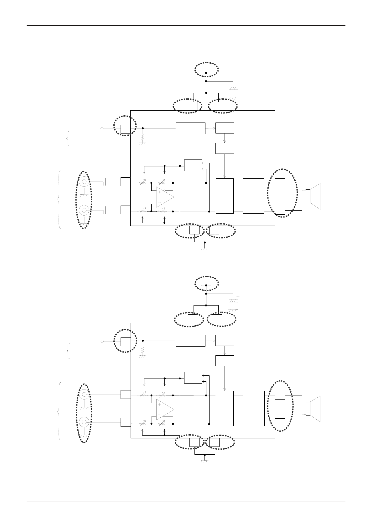
●Application circuit example
SHORT the power supply pin VDD (B1), PVDD (B2) at board pattern, then use singleness power supply.
+Battery
Singleness power supply (+2.5~+5.5V)
Shutdown Control
Shutdown Signal
H :IC Active
L: IC Shutdown
SDNB
C2
Signal VDD
150k
( Typ.)
B1 B2
VDD PVDD
Shutdown
Control
BIAS
OSC
C 3
10 uF
Power VDD
Differential
Input
udio
Input +
0.1uF
udio
Input-
Audio Differential Input
0.1uF
IN+
IN-
C1
Ri
1
Ri
Signal GND
R
LC
2 B 3
PWM
PGNDGND
HBridge
Power GND
Fig1. Differential Input(With Input Coupling Capacitor)
+Battery
Singleness power supply(+2.5~+5.5V)
Shutdown Control
Shutdown Signal
H :IC Active
L : IC Shutdown
SDNB
C2
Signal VDD
150k
Typ.)
(
B1 B2
VDD PVDD
Shutdown
Control
BIAS
OSC
C 3
10 uF
Power VDD
Differential
Input
udio
Input +
udio
Input -
Audio Differential Input
IN+
IN-
C1
Ri
1
Ri
R
Signal GND
LC
2 B3
PWM
PGNDGND
HBridge
Power GND
Fig2. Differential Input(Without Input Coupling Capacitor)
Technical Note
Class-D BTL Output
OUT +
C3
OUT -
Class-D BTL Output
OUT +
C3
OUT -
www.rohm.com
5/19
© 2010 ROHM Co., Ltd. All rights reserved.
2010.09 - Rev.
Page 6
BD5466GUL
A
A
A 3A
A
fRf
A
A
A
A
A
f
f
A
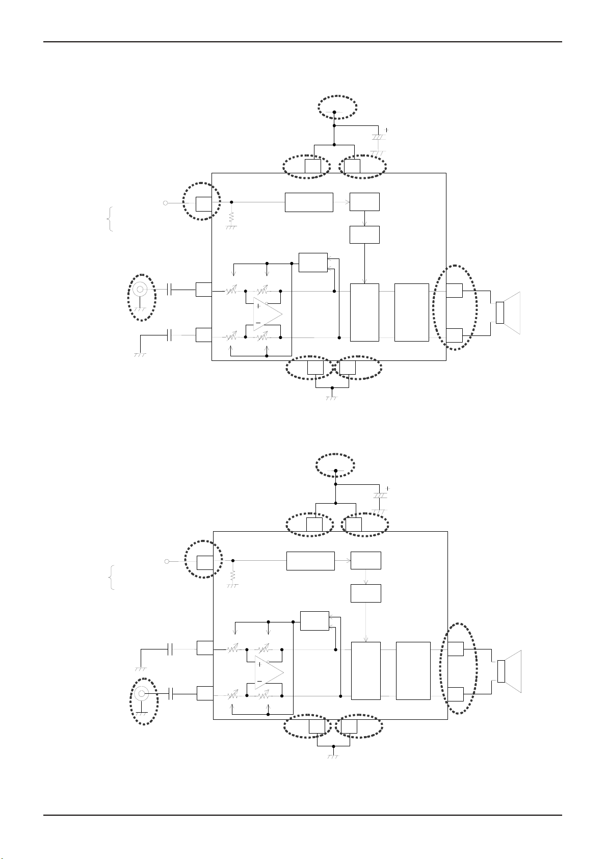
Audio Single End Input
Audio Single End Input
Shutdown Control
Shutdown Signal
H :IC Active
IC Shutdown
L :
udio
Input
Shutdown Control
Shutdown Signal
H :
IC Active
IC Shutdown
L:
udio
Input
0.1uF
0.1uF
0. 1uF
0. 1uF
Technical Note
+Battery
Signal VDD
B1 B2
VDD PVDD
SDNB
C 2
IN +
1
IN -
C 1
Ri
Ri
150k
Typ)
(
Signal GND
Shutdown
Control
LC
R
2 B3
Fig3. Single end input (during IN+ input)
+Battery
B1 B2
VDD PVDD
SDNB
C2
IN +
1
IN -
C1
Ri
Ri
150k
Typ.)
(
Signal GND
Shutdown
Control
LC
R
R
2 B3
Fig4. Single end input (during IN- Input)
Singleness power supply (+2.5~+5.5V)
C3
10uF
Power GND
Power GND
Power VDD
H-
Bridge
C3
10uF
Power VDD Signal VDD
HBridge
BIAS
OSC
PWM
PGNDGND
Singleness power supply (+2.5~+5.5V)
BIAS
OSC
PWM
PGNDGND
Class-D BTL Output
OUT +
C3
OUT -
Class-D BTL Output
OUT +
C 3
OUT -
3
www.rohm.com
6/19
© 2010 ROHM Co., Ltd. All rights reserved.
2010.09 - Rev.
Page 7

BD5466GUL
A
Technical Note
●About the difference of differential input and single end input
・BD5466GUL uses full differential amplifier.
BD5466GUL is a Class-D but, in relation to Audio Input and Output, is same with the conventional Class-AB Amplifier.
For simplicity purposes of the diagram, the Class-D amplifier output stage is omitted in the following explanation.
About the resistor, signal on the diagram
Gives meaning to changes of gain setting by means of ALC Control.
1) Differential Input
Audio
Input
Opposite
0V
IN+
A1
phase
OUT-
A3
Audio
Input
0V
(IN+ - IN- )
(OUT+ - OUT- )
C1
IN-
Opposite
phase
C3
OUT+
2) Single end input (during IN+input )
Audio
Input
0V
IN+
Opposite
phase
A1
S
a
m
e
p
h
a
s
e
OUT-
A3
(IN+ - IN- )
(OUT+ - OUT- )
0V
ー
C1
IN-
ー
C3
OUT+
3) Single end input (during IN-input )
0V
ー
IN+
ー
A1
OUT-
A3
Audio
Input
0V
(IN+ - IN- )
o
p
p
O
C1
IN-
s
e
t
i
s
a
h
p
Opposite
phase
e
(OUT+ - OUT- )
C3
OUT+
○About single end input
・Input is possible whether IN+ or IN- Pin.
Don’t make input pin open, through the input coupling capacitor, please connect to GND as seen on the example above.
Audio input pin should make “mute” condition, not “open” condition when you don’t input any signal.
・During single end input IN+ and IN-, there is a difference with the phase relation of input and output.
Because of differential amplifier, if input (IN+ - IN-), output(OUT+ - OUT-), the audio input and output phase relation will
become:
Phase IN+ Input IN- Input
Audio Input ⇒ output (OUT+ - OUT-) Same phase Opposite phase
www.rohm.com
7/19
© 2010 ROHM Co., Ltd. All rights reserved.
2010.09 - Rev.
Page 8

BD5466GUL
A
A
A3A
fRf
A
A
A3A
fRf
Technical Note
○Gain calculation
<
Shutdown Signal
H :IC Active
IC Shutdown
L :
udio Source
Vins
Vins
【Differential Input】
+ Battery
Cs
B1 B 2
VDD PVDD
SDNB
C2
IN+
0 .1 uF
>
Ci
0 .1 uF
Ci
VIN
(= 2V ins )
Ri
1
IN-
C1
Ri
150 k
(Ty p.)
R
Shutdown
Control
ALC
2 B 3
BIAS
OSC
PWM
PGND
OUT+
C3
HBridge
OUT-
GND
Shutdown Signal
H:IC Active
IC Shutdown
L:
< Audio Source>
Vins
SDNB
C2
IN+
0.1uF
0.1uF
1
Ci
VIN
(=Vins )
IN-
C1
Ci
【single end input】
VDD
Shutdown
Control
150 k
(Ty p.)
ALC
Ri
R
Ri
+ Battery
B 1 B 2
2 B 3
BIAS
OSC
PWM
PGND
PVDD
Cs
H-
Bridge
GND
When Input Level is calculated at IC typical and audio source typical, when input coupling capacitor (Ci) value is large
enough, every gain during the differential input and single end input will become:
Typical Input Level Differential Output Single End Output
OUT+
C3
OUT-
IC Formula①
Audio Source Formula② Formula①
1.IC reference(Difference Input, Single End Input): Formula ①
VIN means the Input Voltage between IC Input Pin (IN+, IN-), VOUT means the output voltage between IC Output Pin
(OUT+, OUT-). During differential input and single end input, the gain calculation formula at IC reference which
includes ALC operation is written below:
Gain = 20×log | VOUT/VIN | =+18~+3 (Typ.) [dB] ・・・ Formula①
2.Audio Source reference(Differential Input): Formula ②
When the input level of audio source is Vins, the relation with the input voltage VIN between IC input pin is written
below:
Vins = VIN / 2
During differential input, at audio source reference that includes ALC operation, gain calculation formula will become:
Gain = 20×log | VOUT / Vins | = 20×log | 2×VOUT / VIN | = +25~+9 (Typ.) [dB] ・・・Formula②
3.Audio Source reference (Single End Input): Formula ①
When the Input level of audio source is Vins, the relation with input voltage VIN between IC input pin (IN+,IN-)
becomes:
Vins = VIN
During single end input, at the audio source that includes ALC operation, gain calculation formula becomes:
Gain = 20×log | VOUT / Vins | = 20×log | VOUT / VIN | = +18~+3 (Typ.) [dB] ・・・ Formula①
www.rohm.com
8/19
© 2010 ROHM Co., Ltd. All rights reserved.
2010.09 - Rev.
Page 9

BD5466GUL
A
A
A3A
r
A
f
f
●Audio Input Pin External LPF connection example
Technical Note
■External LPF connection example
The connection example of 1
st
-order LPF which is formed at Resistor R
and Capacitor C
LPF
to the Audio Input Pin
LPF ,
IN+/- (A1, C1 Pin) is shown below. The cut frequency of input LPF, together with the single end input and differential input
is written below:
= 1 / (2×π×R
fc
LPF
LPF×CLPF
) [Hz]
Ex) fc
=10kHz ⇒ C
LPF
=0.01μF, R
LPF
=1.59kΩ
LPF
1) During single end input
When LPF is connected to audio input pin at single end input setting, at start-up characteristics of audio input pin IN+/-,
during start-up with unbalance (power supply ON/OFF, or shutdown ON/OFF), there is a risk that POP sound will occur
so please be careful.
When no audio input, and in order to prevent output noise, please make previous IC “mute” condition, not “open”
condition. Please refer at the same time to POP Sound countermeasure example.
Battery
+
Pop sound
countermeasure
Front IC
Ro
Shutdown Signal
H : IC Active
L: IC Shutdown
Input Impedance
R
LPF
R
LPF
→
C
LPF
B1
VDD
SDNB
C 2
IN
Ci
+
Ri
150k
(Typ.)
Shutdown
Control
LC
R
B2
BIAS
OSC
1
C
LPF
Ci
-
IN
C 1
Ri
R
GND PGND
PWM
2 B3
Cs
PVDD
OUT +
C3
HBridge
OUT -
Speake
www.rohm.com
9/19
© 2010 ROHM Co., Ltd. All rights reserved.
2010.09 - Rev.
Page 10

BD5466GUL
A
A
A 3A
A
g
f
f
2) Differential Input
+Battery
Cs
Shutdown Signal
H : IC Active
L: IC Shutdown
Front IC
Ro
Input Impedance
LPF
R
LPF
Ro
R
LPF
C
C
LPF
LPF
Ci
Ci
SDNB
C 2
IN+
IN-
C 1
Shutdown
Control
150k
(Typ.)
Ri
1
Ri
B1
VDD
LC
R
R
GND PGND
B2
2 B3
PVDD
BIAS
OSC
PWM
HBrid
OUT +
C 3
e
OUT
■Caution during External LPF Setting
External LPF Resistor R
The bigger the resistor value of LPF resistor R
which is composed of IC input resistor Ri, forms input impedance.
LPF
the more it will decrease the gain.
LPF,
When the input capacitor Ci has enough large capacity value, the relation among external LPF resistor R
IC input resistor Ri and Gain will become:
Gain = 20×log | Rf / (Ri + R
) | [dB]
LPF
Input resistor Ri of BD5466GUL and resistor value of feedback resistor Rf will become the following below,
during ALC operation, changes at ±1dB step, and becomes 16 stages switch specs.
#1. Ri=33.5kΩ(Typ.), Rf=266.5kΩ(Typ.)@Gain=18dB
#2. Ri=37kΩ(Typ.), Rf=263kΩ(Typ.)@Gain=17dB
#3. Ri=41kΩ(Typ.), Rf=259kΩ(Typ.)@Gain=16dB
↓
#15. Ri=116kΩ(Typ.), Rf=184kΩ(Typ.)@Gain=4dB
#16. Ri=124kΩ(Typ.), Rf=176kΩ(Typ.)@Gain=3dB
Also with the driver ability of previous IC step, after checking, constant setting of external LPF and Resistor R
Technical Note
-
LPF
Speaker
and
LPF.
www.rohm.com
10/19
© 2010 ROHM Co., Ltd. All rights reserved.
2010.09 - Rev.
Page 11

BD5466GUL
A
●Evaluation Board Circuit Diagram
Connect to GND
Differential
Input
Shutdown Signal
H:IC Active
L:IC Shutdown
Audio Input
Audio
Input+
Audio
Input-
0.1uF
C2
0.1uF
C1
SDNB
VDD
C2
150k
(Typ.)
IN+
Ri
A1
IN-
C1
Rf
Ri
Rf
GND
VDD
B1
ALC
A2 B3
B2
BIAS
OSC
PWM
PGNDGND
VDD PVDD
Shutdown
Control
C3
10uF
HBridge
OUT+
C3
OUT-
A3
Connect to input signal
※Power Supply terminals VDD(B1), PVDD(B2) are SHORT in the board pattern and use a single power.
●Evaluation Board Parts List
Technical Note
Connect to Power Supply
(VDD=+2.5~5.5V)
BD5466GUL
Connect to Speaker
Qty. Item Description SMD Size
2 C1, C2 Capacitor, 0.1μF 0603
1 C3 Capacitor, 10μF A (3216)
1 S1 Slide Switch 4mm X 10.2mm
1 U1
1 PCB1
IC, BD5466GUL,
Mono Class-D Audio Amplifier
Printed-Circuit Board,
BD5466GUL EVM
1.7mm X 1.7mm
WLCSP Package
― ―
Manufacturer/
Part Number
Murata
GRM188R71C104KA01D
ROHM
TCFGA1A106M8R
NKK
SS-12SDP2
ROHM
BD5466GUL
●About the external part
①Input coupling capacitor (C1, C2)
Input coupling capacitor is 0.1μF.
Input impedance during maximum gain 18dB is 33.5kΩ (Typ.). A high-pass filter is composed by the input coupling
capacitor and the input impedance.
Cut-off frequency”fc” by the formula below, through input coupling capacitor C1(=C2) and input impedance Ri.
fc
1
[Hz]
C1Ri2π
In case of Ri=33.5kΩ, C1(=C2)=0.1μF, cut-off frequency is about 48Hz
②Power Supply Decoupling Capacitor (C3)
Power Supply Decoupling Capacitor is 10uF. When the capacity value of Power Supply Decoupling Capacitor is made
small, it will have an influence to the audio characteristics. When making it small, be careful with the audio characteristics
at actual application. ESR (equivalent series resistor) is low enough; please use capacitor with capacity value of 1μF or
more.
www.rohm.com
11/19
© 2010 ROHM Co., Ltd. All rights reserved.
2010.09 - Rev.
Page 12

BD5466GUL
A
●Evaluation Board PCB Layer
Technical Note
TOP Layer Silk Pattern
BD5466GUL
TOP Layer
Bottom Layer
www.rohm.com
12/19
© 2010 ROHM Co., Ltd. All rights reserved.
2010.09 - Rev.
Page 13

BD5466GUL
A
Technical Note
●About IC Thermal Design
The IC Characteristics has a big relation with the temperature that will be used, to exceed the maximum tolerance junction
temperature, can deteriorate and destroy it. Instant destruction and long-time operation, from these 2 standpoints, there is a
need to be careful with regards to IC thermal. Please be careful with the next points.
The absolute maximum rating of IC shows the maximum junction temperature (Tj
MAX.) or the operation temperature range
(Topr), so refer to this value, use Pd-Ta characteristics (Thermal reduction ratio curve). If input signal is excessive at a state
where heat radiation is not sufficient, there will be TSD(Thermal Shutdown)
For TSD, the chip temperature operates at around 180℃, releases if its around 120℃ or less. Since the aim is to prevent
damage on the chip, please be careful because the long use time at the vicinity where TSD operates can deteriorate the
dependency of the IC.
Thermal Reduction Ratio Curve
Reference Data
VCSP50L1
2.0
Measurement Condition : ROHM Typical Board Mount
Board Size : 50mmx58mm
1.5
1.0
Power Dissipation Pd(W)
0.5
0.69W
θja = 181.8℃/W
0.0
0 25 50 75 100 125
85
Perimeter Temperature Ta(℃)
150
Note : This value is the real measurement, but not the guaranteed value.
The value of power dissipation changes based on the board that will be mounted.
The power dissipation of main IC during the heat dissipation design of many mounted boards, will become bigger than
the value of the above graph.
www.rohm.com
13/19
© 2010 ROHM Co., Ltd. All rights reserved.
2010.09 - Rev.
Page 14

BD5466GUL
A
y
)
Technical Note
Evaluation data - T
●Evaluation data – Typical characteristics (1/4)
90
80
70
60
50
40
Efficiency [%]
30
20
10
0
0 0.1 0.2 0.3 0.4 0.5 0.6 0.7 0.8 0.9 1 1.1 1.2
VDD = 3.6V
VDD = 2.5V
300
250
200
150
Icc [mA]
100
50
0
0 0.1 0.2 0.3 0.4 0.5 0.6 0.7 0.8 0.9 1 1.1 1.2
Supply Current vs Output power
VDD = 2.5V
0.3
0.25
0.2
0.15
Pd [W]
0.1
0.05
0
0 0.1 0.2 0.3 0.4 0.5 0.6 0.7 0.8 0.9 1 1.1 1.2
Power dissipation vs Output power
VDD = 2.5V
5.0
4.5
4.0
3.5
3.0
2.5
[mA]
CC
I
2.0
1.5
1.0
0.5
0.0
0123456
Supply Current vs Power Supply
pical Characteristics (1/4
Efficiency - Output power
f=1kHz, RL=8Ω+33uH
VDD = 5.0V
Output Power [W]
Fig.5
Figure.1 Figure.2
f=1kHz, RL=8Ω+33uH
VDD = 5.0V
VDD = 3.6V
Output Power [W]
Fig.7
Figure.3 Figure.4
f=1kHz, RL=8Ω+33uH
VDD = 3.6V
Output Power [W]
Figure.5 Figure.6
Fig.9
RL=No load, No signal
VDD [V]
Fig.11
Figure.7 Figure.8
VDD = 5.0V
VDD=2.5V
VDD=3.6V
VDD=5.0V
VDD=2.5V
VDD=3.6V
VDD=5.0V
VDD=2.5V
VDD=3.6V
VDD=5.0V
Efficiency vs Output power
80
70
VDD = 2.5V
60
50
40
30
Efficiency [%]
20
10
0
0 0.2 0.4 0.6 0.8 1 1.2 1.4 1.6 1.8 2
f=1kHz, RL=4Ω+33uH
VDD = 3.6V
VDD = 5.0V
Output Power [W]
VDD=2.5V
VDD=3.6V
VDD=5.0V
Fig.6
Supply Current vs Output power
450
400
350
300
250
VDD = 2.5V
200
Icc [mA]
150
100
50
0
0 0.2 0.4 0.6 0.8 1 1.2 1.4 1.6 1.8 2
f=1kHz, RL=4Ω+33uH
VDD = 5.0V
VDD = 3.6V
Output Power [W]
VDD=2.5V
VDD=3.6V
VDD=5.0V
Fig.8
Power dissipation vs Output power
0.45
0.40
0.35
0.30
0.25
0.20
Pd [W]
VDD = 2.5V
0.15
0.10
0.05
0.00
0 0.2 0.4 0.6 0.8 1 1.2 1.4 1.6 1.8 2
f=1kHz, RL=4Ω+33uH
VDD = 5.0V
VDD = 3.6V
VDD=2.5V
VDD=3.6V
VDD=5.0V
Output Power [W]
Fig.10
Shutdown Current vs Power Supply
5.0
4.5
4.0
3.5
3.0
2.5
[μA]
SDN
I
2.0
1.5
1.0
0.5
0.0
0123456
RL=No load, No signal
VDD [V]
Fig.12
www.rohm.com
14/19
© 2010 ROHM Co., Ltd. All rights reserved.
2010.09 - Rev.
Page 15

BD5466GUL
A
y
)
Technical Note
Evaluation data - T
●Evaluation data – Typical characteristics (2/4)
2.0
1.8
1.6
1.4
1.2
1.0
0.8
0.6
Output Power [W]
0.4
0.2
0.0
4 8 12 16 20 24 28 32
Output power vs Load Resistance
THD+N=1%, f=1kHz, 400Hz-30kHz BPF
VDD = 5.0V
1.2
Output Power vs Power Supply
RL=8Ω, f=1kHz, 400Hz-30kHz BPF
pical Characteristics (2/4
VDD = 3.6V
RL[Ω]
Figure.9
Fig.13
VDD = 2.5V
1.0
0.8
0.6
0.4
Output Power [W]
0.2
0.0
2 2.5 3 3.5 4 4.5 5 5.5 6
Total Harmonic Distortion + Noise vs Output Power
100
10
RL=8Ω, f=1kHz, 400Hz-30kHz BPF
VDD = 2.5V
VDD = 3.6V
VDD = 5.0V
VDD[V]
Fig.14
Figure.10 Figure.11
VDD = 3.6V
THD+N [%]
1
VDD = 2.5V
VDD = 5.0V
0.1
0.01 0.1 1 10
Output Power [W]
Fig.16 Fig.17
Figure.12 Figure.13
Total Harmonic Distortion + Noise vs Frequency
10
1
VDD=5.0V RL=8Ω, 400Hz-30kHz BPF
Po=25mW
Po=100mW
Po=250mW
Po = 25mW
Po = 100mW
THD+N [%]
0.1
Po = 250mW
0.01
10 100 1k 10k 100k
Frequency [Hz]
Fig.18 Fig.19
Figure.14 Figure.15
VDD=2.5V
VDD=3.6V
VDD=5.0V
THD+N≦1%
Output Power vs Power Supply
2.5
2.0
1.5
1.0
Output Power [W]
0.5
0.0
RL=4Ω, f=1kHz, 400Hz-30kHz BPF
THD+N≦1%
22.533.544.555.56
VDD[V]
Fig.15
Total Harmonic Distortion + Noise vs Output Power
RL=4Ω, f=1kHz, 400Hz-30kHz BPF
100
10
THD+N [%]
1
0.1
0.01 0.1 1 10
10
THD+N [%]
0.1
0.01
VDD = 2.5V
VDD = 3.6V
VDD = 5.0V
VDD = 2.5V
Total Harmonic Distortion + Noise vs Frequency
VDD=3.6V RL=8Ω, 400Hz-30kHzBPF
Po=25mW
Po=100mW
Po=250mW
1
Po = 25mW
10 100 1k 10k 100k
VDD = 3.6V
VDD = 5.0V
Output Power [W]
Po = 100mW
Po = 250mW
Frequency [Hz]
www.rohm.com
15/19
© 2010 ROHM Co., Ltd. All rights reserved.
2010.09 - Rev.
Page 16

BD5466GUL
A
y
)
Technical Note
Evaluation data - T
●Evaluation data – Typical characteristics (3/4)
Total Harmonic Distortion + Noise vs Frequency
VDD=2.5V, RL=8Ω, 400Hz-30kHz BPF
10
Po=25mW
Po=100mW
1
THD+N [%]
0.1
Po=150mW
Po = 25mW
pical Characteristics (3/4
Po = 100mW
Po = 150mW
Total Harmonic Distortion + Noise vs Frequency
RL=8Ω, Po=125mW, 400Hz-30kHz BPF
10
1
THD+N [%]
0.1
VDD=2.5V
VDD=3.6V
VDD=5.0V
VDD = 3.6V
VDD = 5.0V
0.01
10 100 1k 10k 100k
Frequency [Hz]
Fig.20
Figure.16 Figure.17
Gain vs Frequency
RL=8Ω, Vin=0.25Vpp, 400Hz-30kHz BPF
20
18
16
14
12
10
Gain [dB]
8
6
4
2
0
10 100 1k 10k 100k
VDD=2.5V
VDD=3.6V
VDD=5.0V
Frequency [Hz]
Fig.22 Fig.23
Figure.18 Figure.19
VDD = 5.0V
VDD = 2.5V
VDD = 3.6V
Output Power vs Input Level @ sweep up
RL=8Ω, f=1kHz, 400Hz-30kHz BPF
10
VDD = 5.0V
1
0.01
10 100 1k 10k 100k
RL=4Ω, Vin=0.25Vpp, 400Hz-30kHz BPF
20
18
16
14
12
10
Gain [dB]
8
6
4
2
0
10 100 1k 10k 100k
VDD=2.5V
VDD=3.6V
VDD=5.0V
Output Power vs Input Level @ sweep up
10
1
VDD = 2.5V
Frequency [Hz]
Fig.21
Gain vs Frequency
VDD = 5.0V
VDD = 2.5V
VDD = 3.6V
Frequency [Hz]
RL=4Ω, f=1kHz, 400Hz-30kHz BPF
VDD = 5.0V
100m
VDD = 2.5V
Output Power [W]
10m
1m
-30 -25 -20 -15 -10 -5 0 5
Total Harmonic Distortion + Noise vs Input Level @ sweep up
100
10
RL=8Ω,f=1kHz, 400Hz-30kHz BPF
VDD = 2.5V
VDD = 3.6V
VDD = 5.0V
Vin [dBV]
Fig.24 Fig.25
Figure.20 Figure.21
VDD = 2.5V
VDD = 3.6V
VDD = 5.0V
VDD = 3.6V
1
THD+N [%]
0.1
www.rohm.com
16/19
© 2010 ROHM Co., Ltd. All rights reserved.
0.01
-30 -25 -20 -15 -10 -5 0 5
VDD = 2.5V
VDD = 3.6V VD D = 5.0V
Vin [dBV]
Fig.26 Fig.27
Figure.22 Figure.23
100m
Output Power [W]
10m
1m
-30 -25 -20 -15 -10 -5 0 5
Total Harmonic Distortion + Noise vs Input Level @ sweep up
100
10
THD+N [%]
1
0.1
-30 -25 -20 -15 -10 -5 0 5
RL=4Ω,f=1kHz, 400Hz-30kHz BPF
VDD = 2.5V
VDD = 3.6V
VDD = 5.0V
VDD = 2.5V
VDD = 2.5V
Vin [dBV]
Vin [dBV]
VDD = 3.6V
VDD = 2.5V
VDD = 3.6V
VDD = 5.0V
VDD = 3.6V
VDD = 5.0V
2010.09 - Rev.
Page 17

BD5466GUL
A
y
)
Technical Note
●Evaluation data – Typical characteristics (4/4)
Evaluation data - T
ALC Limit Operation Waveform
2V / Div.
pical Characteristics (4/4
f=1kHz
INPUT
OUTPUT
-101234567
1V / Div.
Time [msec]
Fig.28
Figure.24 Figure.25
Waveform during Start-up
INPUT
OUTPUT
Ton ( Wake-up Time)
-0.2 0 0.2 0.4 0.6 0.8 1 1.2 1.4
Time [msec]
Fig.30
Figure.26 Figure.27
ALC Release Operation Waveform
2V / Div.
INPUT
OUTPUT
-10 0 10 20 30 40 50 60 70
f=1kHz
Time [msec]
Fig.29
Waveform during Shutdown
1V / Div.
INPUT
OUTPUT
-0.2 0 0.2 0.4 0.6 0.8 1 1.2 1.4
Time [msec]
Fig.31
www.rohm.com
17/19
© 2010 ROHM Co., Ltd. All rights reserved.
2010.09 - Rev.
Page 18

BD5466GUL
A
●Notes for use
(1) The numerical value and the data of the mention are a design representative value and are not the one which guarantees
the value.
(2) It is convinced that it should recommend application circuit example but in case of use, we request the confirmation of the
characteristic more sufficiently. When changing an external part fixed number and becoming use, it considers sprawl of
the external part and our company's LSI including the transition characteristic in addition to the stillness characteristic and
so on, see and fix an enough margin.
(3) Absolute maximum ratings
This IC may be damaged if the absolute maximum ratings for the applied voltage, temperature range, or other
parameters are exceeded. Therefore, avoid using a voltage or temperature that exceeds the absolute maximum ratings.
If it is possible that absolute maximum ratings will be exceeded, use fuses or other physical safety measures and
determine ways to avoid exceeding the IC's absolute maximum ratings.
(4) GND terminal’s potential
Try to set the minimum voltage for GND terminal’s potential, regardless of the operation mode.
(5) Shorting between pins and mounting errors
When mounting the IC chip on a board, be very careful to set the chip's orientation and position precisely. When the
power is turned on, the IC may be damaged if it is not mounted correctly. The IC may also be damaged if a short occurs
(due to a foreign object, etc.) between two pins, between a pin and the power supply, or between a pin and the GND.
(6) Operation in strong magnetic fields
Note with caution that operation faults may occur when this IC operates in a strong magnetic field.
(7) Thermal design
Ensure sufficient margins to the thermal design by taking in to account the allowable power dissipation during actual use
modes, because this IC is power amplifier. When excessive signal inputs which the heat dissipation is insufficient
condition, it is possible that thermal shutdown circuit is active.
(8) Thermal shutdown circuit
This product is provided with a built-in thermal shutdown circuit. When the thermal shutdown circuit operates, the output
transistors are placed under open status. The thermal shutdown circuit is primarily intended to shut down the IC avoiding
thermal runaway under abnormal conditions with a chip temperature exceeding T
protect and secure an electrical appliance.
(9) Load of the output terminal
This IC corresponds to dynamic speaker load, and doesn't correspond to the load except for dynamic speakers. When
using speaker load 8Ω or less (especially 4Ω), there will be a risk of generating distortion at the speaker output wave form
during ALC limit operation.
(10) The short protection of the output terminal
This IC is built in the short protection for a protection of output transistors. When the short protection is operated, output
terminal become Hi-Z condition and is stopped with latch. Once output is stopped with latch, output does not recover
automatically by canceling the short-circuiting condition. The condition of stopping with latch is cancelled, when power
supply or mute signal is turned off and turned on again.
(11) Operation Range
The rated operating power supply voltage range (VDD=+2.5V~+5.5V) and the rated operating temperature range
(Ta=-40℃~+85℃) are the range by which basic circuit functions is operated. Characteristics and rated output power are
not guaranteed in all power supply voltage ranges or temperature ranges.
(12) Electrical Characteristics
Every audio characteristics list of the limit output power, total harmonic distortion, maximum gain, ALC limit level, ALC
release level etc. shows the typical characteristics of the device, highly dependent to the board lay-out, parts to be used,
power supply. The value when the device and each component are directly mounted to the board of Rohm.
(13) Power Supply
Since the Power Supply Pin for signal (VDD) and power supply for Power (PVDD) is SHORT at internal, short the board
pattern, then use a single power supply. Also, the power supply line of class-D speaker amplifier flows big peak energy. It
will influence the audio characteristics based on the capacity value of power supply decoupling capacitor, arrangement.
For the power supply decoupling capacitor, please arrange appropriately the low capacity (1μF or more) of ESR
(equivalent series resistor) directly near to IC Pin.
(14) ALC (A
utomatic Level Control) Function
The ALC automatically adjusts the audio output level, and a function that prevents the over output to the speaker. When
ALC function is working, gain switches at zero-cross point of audio output normally. If the time that audio output reaches
to zero-cross point is long, gain switches at about 1msec later (attack time), at about 25msec later (release time). So,
attack time and release time will change at audio input frequency. ALC parameter is fixed. The system does not
correspond to noise of impulse. Also, ALC limit control will become a power supply tracking type, limit output power is
dependent to power supply voltage. The ALC characteristics of limit output power, ALC limit and release limit will be
influenced by the shaking so please be careful.
=+150℃, and is not intended to
jmax
Technical Note
www.rohm.com
18/19
© 2010 ROHM Co., Ltd. All rights reserved.
2010.09 - Rev.
Page 19

BD5466GUL
A
●Ordering part number
B D 5 4 6 6 G U L - E 2
Technical Note
Part No. Part No. Package
VCSP50L1
(BD5466GUL)
1PIN MARK
9-φ0.25±0.05
0.05
(φ0.15)INDEX POST
BA
0.35±0.05
C
B
A
1.70±0.05
1
P=0.5×2
0.06 S
A
3
2
1.70±0.05
0.1±0.05
0.55MAX
S
0.35±0.05
B
P=0.5×2
(Unit : mm)
GUL: VCSP50L1
<Tape and Reel information>
Embossed carrier tapeTape
Quantity
Direction
of feed
3000pcs
E2
The direction is the 1pin of product is at the upper left when you hold
()
reel on the left hand and you pull out the tape on the right hand
Reel
1pin
Packaging and forming specification
E2: Embossed tape and reel
Direction of feed
Order quantity needs to be multiple of the minimum quantity.
∗
www.rohm.com
19/19
© 2010 ROHM Co., Ltd. All rights reserved.
2010.09 - Rev.
Page 20

Notes
No copying or reproduction of this document, in part or in whole, is permitted without the
consent of ROHM Co.,Ltd.
The content specied herein is subject to change for improvement without notice.
The content specied herein is for the purpose of introducing ROHM's products (hereinafter
"Products"). If you wish to use any such Product, please be sure to refer to the specications,
which can be obtained from ROHM upon request.
Examples of application circuits, circuit constants and any other information contained herein
illustrate the standard usage and operations of the Products. The peripheral conditions must
be taken into account when designing circuits for mass production.
Great care was taken in ensuring the accuracy of the information specied in this document.
However, should you incur any damage arising from any inaccuracy or misprint of such
information, ROHM shall bear no responsibility for such damage.
The technical information specied herein is intended only to show the typical functions of and
examples of application circuits for the Products. ROHM does not grant you, explicitly or
implicitly, any license to use or exercise intellectual property or other rights held by ROHM and
other parties. ROHM shall bear no responsibility whatsoever for any dispute arising from the
use of such technical information.
Notice
The Products specied in this document are intended to be used with general-use electronic
equipment or devices (such as audio visual equipment, ofce-automation equipment, communication devices, electronic appliances and amusement devices).
The Products specied in this document are not designed to be radiation tolerant.
While ROHM always makes effor ts to enhance the quality and reliability of its Products, a
Product may fail or malfunction for a variety of reasons.
Please be sure to implement in your equipment using the Products safety measures to guard
against the possibility of physical injury, re or any other damage caused in the event of the
failure of any Product, such as derating, redundancy, re control and fail-safe designs. ROHM
shall bear no responsibility whatsoever for your use of any Product outside of the prescribed
scope or not in accordance with the instruction manual.
The Products are not designed or manufactured to be used with any equipment, device or
system which requires an extremely high level of reliability the failure or malfunction of which
may result in a direct threat to human life or create a risk of human injury (such as a medical
instrument, transportation equipment, aerospace machinery, nuclear-reactor controller, fuelcontroller or other safety device). ROHM shall bear no responsibility in any way for use of any
of the Products for the above special purposes. If a Product is intended to be used for any
such special purpose, please contact a ROHM sales representative before purchasing.
If you intend to export or ship overseas any Product or technology specied herein that may
be controlled under the Foreign Exchange and the Foreign Trade Law, you will be required to
obtain a license or permit under the Law.
Thank you for your accessing to ROHM product informations.
More detail product informations and catalogs are available, please contact us.
ROHM Customer Support System
www.rohm.com
© 2010 ROHM Co., Ltd. All rights reserved.
http://www.rohm.com/contact/
R1010
A
 Loading...