

Page 1
Small-sized Class-D Speaker Amplifiers
Analog Input
Monaural Class-D Speaker Amplifier
BD5460GUL
●Description
BD5460GUL is a low voltage drive class-D monaural speaker amplifier that was developed for cellular phones, mobile
audio products and the others.LC-filter of speaker output is unnecessary, and the number of external components is three.
It is suitable for the application of battery drive because of high efficiency and low power consumption.
Also, stand-by current is 0µA (typ.), and fast transitions from standby to active with little pop noise. It is suitable for
applications that switch repeatedly between stand-by and active.
●Features
1) No LC filter required
2) Only three external components
3) High power 2.5W/4Ω/BTL (VDD=5V, RL=4Ω, THD+N=10%, typ.)
4) High power 0.85W/8Ω/BTL (VDD=3.6V, RL=8Ω, THD+N=10%, typ.)
5) Gain 6dB
6) Analog differential input / PWM digital output
7) Pop noise suppression circuitry
8) Built-in standby function
9) Protection circuitry (Short protection [Auto recover without power cycling], Thermal shutdown, Under voltage lockout)
10) Very small package 9-Bump WL-CSP (1.6*1.6*0.55mmMAX)
●Applications
Mobile phones, Mobile electronics applications
●Absolute Maximum Ratings(Ta=25℃)
Item Symbol Ratings Unit
Power Supply Voltage
Power Dissipation
Storage Temperature Range
STBY Terminal Input Range
IN+, IN- Terminal Input Range
*1 When mounted on a 50 mm×58mm Rohm standard board, reduce by 5.52 mW/°C above Ta = +25 °C.
●Operating Conditions
Item Symbol Ratings Unit
Power Supply Voltage VDD +2.5 ~ +5.5 V
Temperature Range Topr -40 ~ +85 ℃
※ This product is not designed for protection against radioactive rays
VDD
Pd
Ts tg
Vstby
Vin
7.0
690 *1
-55 ~ +150
-0.1~VDD+0.1
-0.1~VDD+0.1
V
mW
℃
V
V
No.10101EAT01
www.rohm.com
© 2010 ROHM Co., Ltd. All rights reserved.
1/16
2010.06 - Rev.A
Page 2
BD5460GUL
Technical Note
●Electric Characteristics
(Unless otherwise specified, Ta=25℃, VDD=3.6V, f=1kHz, RL=8Ω, AC item=LC Filter ; L=22µH, C=1µF )
Parameter Symbol
MIN. TYP. MAX.
Limits
Unit Conditions
Circuit current (No signal) ICC ― 2.0 4.0 mA Active mode, No load
Circuit current (Standby) I
― 0.1 2 µA Standby mode
STBY
Output power 1 PO1 450 680 ― mW BTL, f=1kHz, THD+N=1% *1
Output power 2 PO2 550 850 ― mW BTL, f=1kHz, THD+N=10% *1
Voltage gain GV 5.4 5.9 6.4 dB BTL
Power Supply Rejection Ratio P
45 53 ― dB BTL,f=1kHz, Vripple=0.1Vpp *2
SRR
Output offset voltage ΔVo -25 0 +25 mV Vin=0V, BTL
Switching Frequency fosc 175 250 325 kHz
Start-up time Ton 0.39 0.51 0.73 msec
Standby input Voltage
Standby input current
*BTL=Bridged Tied Load (Voltage between A3-C3.), *1;B.W.=400~30kHz,*2;DIN AUDIO
High-level V
Low-level V
High-level I
Low-level I
1.4 ― VDD V Active mode
STBYH
0 ― 0.4 V Standby mode
STBYL
6 12 18 µA V
STBYH
-5 0 5 µA V
STBYL
STBY
STBY
=3.6V
=0V
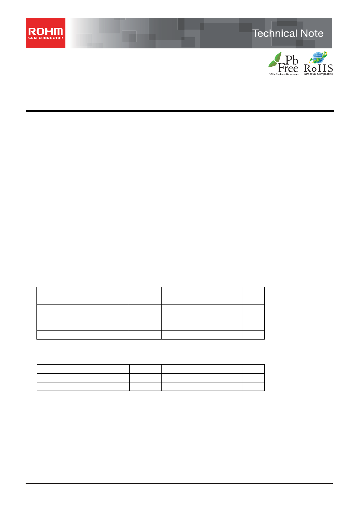
●Measurement Circuit Diagram
A
Vripple
10µ
VDD
VDD
B1 B2
PVDD
VSTBY
A
STBY
C2
Bias OSC
0.1µ
Vin
Vin
0.1µ
IN+
A1
IN-
C1
PWM
HBridge
OUT-
A3
OUT+
C3
22 µ H
1µ
8
22 µ H
1µ
A2GND B3
PGND
●Active / Standby Control
STBY Pin(C2pin)
Mode Pin level Conditions
Active H IC active
Standby L IC shutdown
VSE
V
V
V
BTL
V
VSE
www.rohm.com
© 2010 ROHM Co., Ltd. All rights reserved.
2/16
2010.06 - Rev.A
Page 3
BD5460GUL
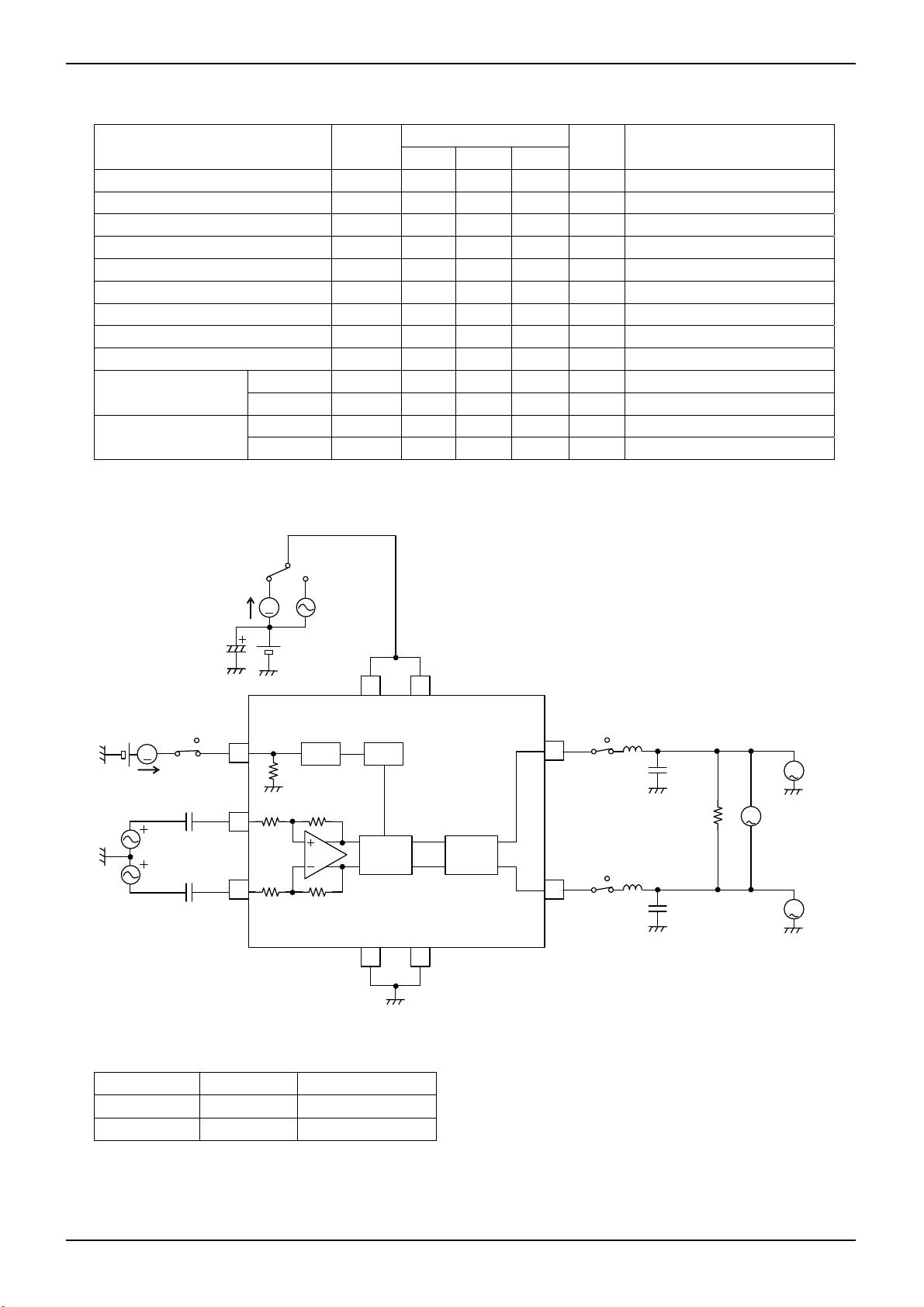
●Package Outlines
●Block Diagram ●Pin Assignment Chart
STBY
C2
IN+
A1
IN-
C1
LOT No.
VDD
Bias OSC
GND
B1
PWM
A2
5460
B2
B3
PVDD
HBridge
PGND
WL-CSP : VCSP50L1
OUT-
A3
OUT+
C3
(unit : mm)
PIN No. PIN 名
A1 IN+
A2 GND
A3 OUT-
B1 VDD
B2 PVDD
B3 PGND
C1 IN-
C2 STBY
C3 OUT+
BOTTOM VIEW TOP VIEW
Technical Note
www.rohm.com
© 2010 ROHM Co., Ltd. All rights reserved.
3/16
2010.06 - Rev.A
Page 4
BD5460GUL
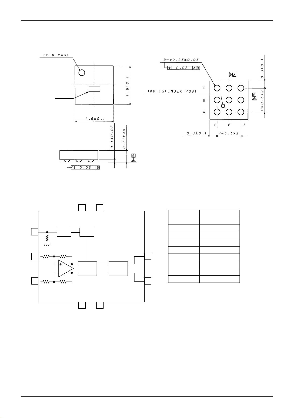
●Application Circuit Example
H:Active
L:Shutdown
Audio
Input+
Differential
Input
Audio
Input-
H:Active
L:Shutdown
Audio
Input+
Differential
Input
Audio
Input-
H:Active
L:Shutdown
Audio
Input
10μ
VDD
B1
B2
PVDD
STBY
C2
IN+
A1
IN-
C1
Bias OSC
PWM
A2GND B3
PGND
Fig.1 Differential input for mobile phone
10μ
VDD
B1
B2 PVDD
STBY
0.1μ
0.1μ
0.1μ
0.1μ
C2
IN+
A1
IN-
C1
Differential input with coupling input capacitors
Fig.2
STBY
C2
IN+
A1
IN-
C1
Bias OSC
PWM
A2GND B3
VDD
B1
Bias OSC
PWM
A2GND B3
PGND
10μ
B2 PVDD
PGND
HBridge
Fig.3 Single-Ended input
HBridge
HBridge
Technical Note
OUTA3
OUT+
C3
OUTA3
OUT+
C3
OUTA3
OUT+
C3
www.rohm.com
© 2010 ROHM Co., Ltd. All rights reserved.
4/16
2010.06 - Rev.A
Page 5
BD5460GUL
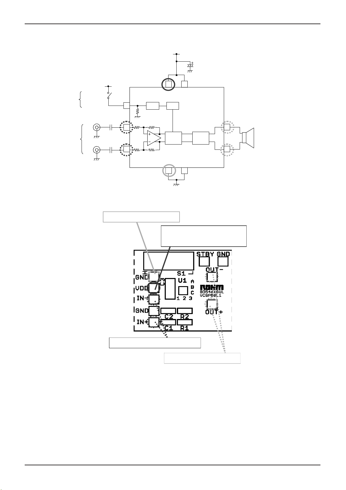
●Evaluation board Circuit Diagram
H:Active
L:Shutdown
Audio
Input+
0.1μ
Differential
Input
Audio
Input-
C2
0.1μ
C1
Please connect to GND line.
VDD
VDD
S1
STB Y
C2
IN+
A1
IN-
C1
U1
300k
Rin =100k
Rin= 100k
B1 B2
Bias OSC
PWM
GND PGND
A2
B3
Please connect to Power Supply
(VDD=+2.5~5.5V) line.
Please connect to Input Signal line.
Please connect to Speaker.
C3
10μ
PVDD
HBridge
Technical Note
OUTA3
OUT+
C3
www.rohm.com
© 2010 ROHM Co., Ltd. All rights reserved.
5/16
2010.06 - Rev.A
Page 6

BD5460GUL
●Evaluation board Parts List
Qty. Item Description SMD Size
2 C1, C2 Capacitor, 0.1µF 0603
1 C3 Capacitor, 10µF A (3216)
1 S1 Slide Switch 4mm X 10.2mm
1 U1
1 PCB1
●Description of External components
Input coupling capacitor (C1,C2)
①
It makes a Input coupling capacitor 0.1µF.
Input impedance is 100kΩ (Typ.).
It sets cut-off frequency fc by the following formula by input coupling capacitor C1 (=C2) and input impedance Ri.
fc
In case of Ri =100kΩ, C1 (=C2) =0.1µF, it becomes fc = about 16 Hz.
② Power decoupling capacitor (C3)
It makes a power decoupling capacitor 10 µF.
When making capacitance of the power decoupling capacitor, there is an influence in the Audio characteristic.
When making small, careful for the Audio characteristic at the actual application.
1
IC, BD5460GUL,
Mono Class-D audio amplifier
Printed-circuit board,
BD5460GUL EVM
[Hz]
C1Ri2π
1.6mm X 1.6mm
WLCSP Package
― ―
Murata
GRM188R71C104KA01D
ROHM
TCFGA1A106M8R
NKK
SS-12SDP2
ROHM
BD5460GUL
Manufacturer/
Part Number
Technical Note
www.rohm.com
© 2010 ROHM Co., Ltd. All rights reserved.
6/16
2010.06 - Rev.A
Page 7

BD5460GUL
●Evaluation board PCB layer
Technical Note
TOP Layer silk pattern
TOP Layer
Bottom Layer
www.rohm.com
© 2010 ROHM Co., Ltd. All rights reserved.
7/16
2010.06 - Rev.A
Page 8

BD5460GUL
Technical Note
●The way of evaluating audio characteristic
Evaluation Circuit Diagram
VDD
C3
0.1μ
C4
10μ
H:Active
L:Shutdown
Audio
Inp ut+
Diffe rent ial
Inp ut
Audio
Inp ut-
VDD
0.1μ
C2
0.1μ
C1
STBY
C2
IN+
A1
IN-
C1
300k
Ri=100k
Ri=100k
VDD PVDD
Bias OSC
B1
PWM
B2
HBridge
OUT-
A3
OUT+
C3
22μH
22μH
1μF
1μF
Measument Instrumen
-
R
BTL
L
+
GND PGND
A2
B3
RL=Speaker Load
When measuring audio characteristics, insert LC filter during the output terminal of IC and the speaker load and measure it.
Arrange LC filter as close as possible to the output terminal of IC.
In case of L=22µH, C=1µF, the cut-off frequency becomes the following.
fc
1
LCπ2
1
μF1μH22π2
kHz34
Use a big current type - Inductor L.
(Reference)
TDK: SLF12575T-220M4R0
Audio
Precision
etc
www.rohm.com
© 2010 ROHM Co., Ltd. All rights reserved.
8/16
2010.06 - Rev.A
Page 9
BD5460GUL
Technical Note
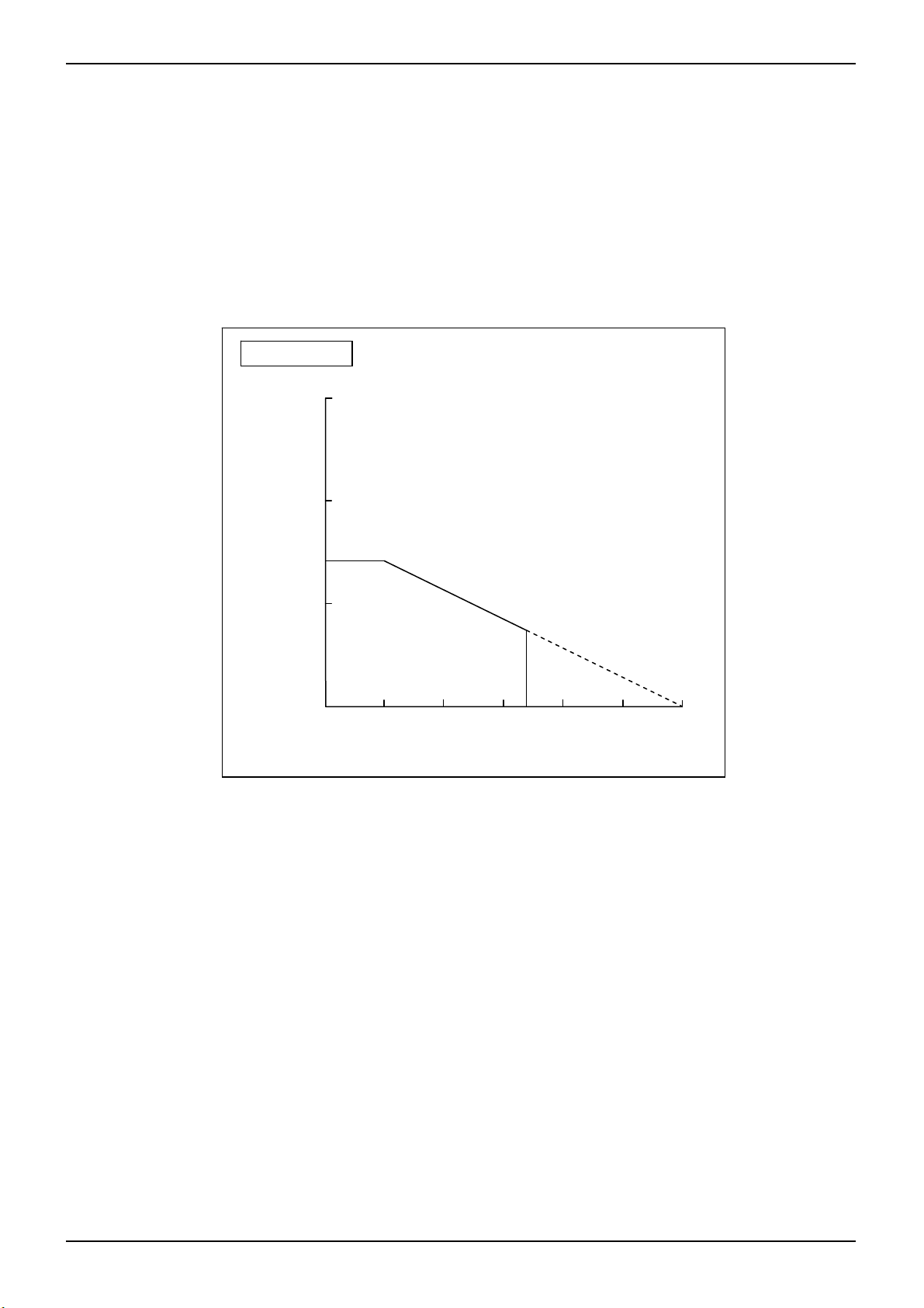
●About the thermal design by the IC
Characteristics of an IC have a great deal to do with the temperature at which it is used, and exceeding absolute maximum
ratings may degrade and destroy elements. Careful consideration must be given to the heat of the IC from the two
standpoints of immediate damage and long-term reliability of operation. Pay attention to points such as the following.
Since an maximum junction temperature (Tjmax.) or operating temperature range (Topr) is shown in the absolute maximum
ratings of the IC, to reference the value, find it using the Pd-Ta characteristic (temperature derating curve).
If an input signal is too great when there is insufficient radiation, TSD (thermal shutdown) may operate.
TSD, which operates at a chip temperature of approximately +180
℃.Since TSD operates persistently with the purpose of preventing chip damage, be aware that long-term use in the
+100
℃, is canceled when this goes below approximately
vicinity that TSD affects decrease IC reliability.
Temperature Derating Curve
Reference data
1.5
measurement conditions : IC unit and Rohm standard board mount
board size : 50mm×58mm
1.0
0.69W
Power Dissipation Pd (W)
0.5
θja = 181.8℃/W
0.0
0 25 50 75 100 125
85
150
Note) Values are actual measurements and are not guaranteed.
Ambient Temperature Ta(
℃)
Power dissipation values vary according to the board on which the IC is mounted. The Power dissipation of this IC when
mounted on a multilayer board designed to radiate is greater than the values in the graph above.
www.rohm.com
© 2010 ROHM Co., Ltd. All rights reserved.
9/16
2010.06 - Rev.A
Page 10

BD5460GUL
●Typical Characteristics
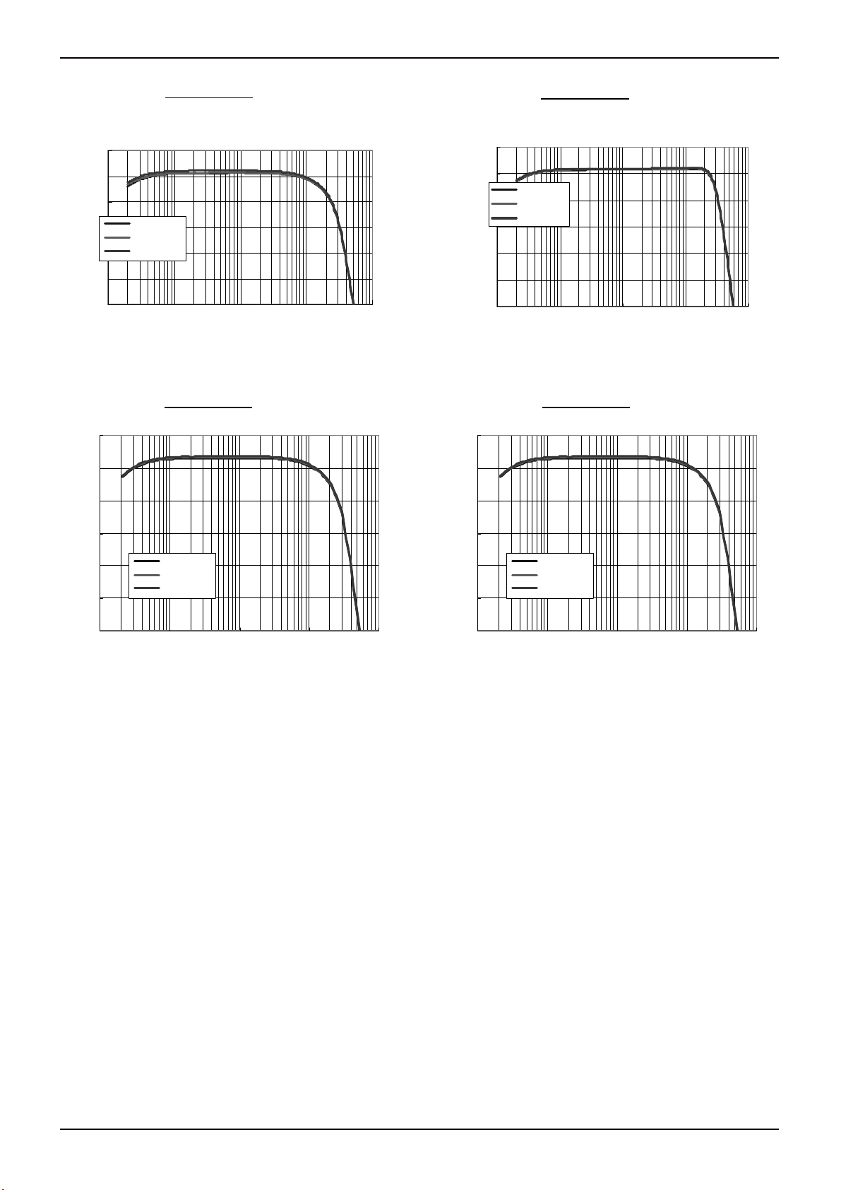
Table of graphs
Efficiency vs Output power 4, 6
Supply current (Icc)
Shutdown current (Istby) vs Supply voltage 9
Output power (Po)
Items Parameter Figure
vs Output power 5, 7
vs Supply voltage 8
vs Load resistance 10, 11
vs Supply voltage 12
vs Output power 13, 14
Technical Note
Total harmonic distortion plus noise (THD+N)
Supply voltage rejection ratio (PSRR) vs Frequency 20, 21, 22, 23
Common-mode rejection ratio (CMRR) vs Frequency 24
Gain vs Frequency 28, 29, 30, 31
vs Frequency 15, 16, 17, 18, 25, 26, 27
vs Common-mode input voltage 19
www.rohm.com
© 2010 ROHM Co., Ltd. All rights reserved.
10/16
2010.06 - Rev.A
Page 11

BD5460GUL
●Reference data
Efficie nc y [%]
f=1kHz RL=8Ω+33uH LC-filter(22uH+1uF)
100
90
80
70
60
50
40
30
20
10
0
0 0.1 0 .2 0.3 0.4 0.5 0.6 0 .7 0 .8 0 .9 1 1.1 1.2
f=1 kHz RL= 4Ω+33 uH L C-filt er(22 uH+ 1uF)
90
80
70
60
50
40
30
Efficiency [%]
20
10
0
0 0.2 0.4 0.6 0.8 1 1.2 1.4 1.6 1.8 2
3
2.5
2
1.5
Icc [mA]
1
0.5
0
0123456
f=1kHz LC- filter(22 uH +1 uF ) 40 0H z-3 0k Hz
2.8
2.4
2.0
1.6
1.2
Po [W]
0.8
0.4
0.0
4 8 12 16 20 24 28 32
Efficiency - Output power
Po [W]
Fig.4
Efficiency vs Output power
Po [W]
Fig.6 Fig.7
Ic c - VDD
No load, N o signal
VDD [V]
Fig.8 Fig.9
Output power vs RL THD+N=10%
VDD=2 .5V
VDD=3 .6V
VDD=5 .0V
RL [Ω]
Fig.10
VDD=2.5V
VDD=3.6V
VDD=5.0V
VDD=2 .5V
VDD=3 .6V
VDD=5 .0V
Technical Note
300
250
200
150
Icc [mA]
100
f=1kHz RL=8Ω+33uH LC-filter(22uH+1uF)
50
0
0 0.10.20.3 0.40.5 0.60.70.80.9 1 1.11.2
f=1 kHz RL= 4Ω+33 uH L C-filt er(22 uH+ 1uF)
600
500
400
300
Icc [mA]
200
100
0
0 0 .2 0.4 0 .6 0.8 1 1 .2 1.4 1 .6 1.8 2
0.5
0.4
0.3
0.2
Istby [uA]
0.1
0
0123456
f=1kHz LC- filter(22 uH +1 uF ) 40 0H z-3 0k Hz
1.8
1.6
1.4
1.2
1.0
0.8
Po [W]
0.6
0.4
0.2
0.0
4 8 12 16 20 24 28 32
Icc vs Output power
VDD=2 .5V
VDD=3 .6V
VDD=5 .0V
Po [W]
Fig.5
Icc vs Output power
VDD=2.5V
VDD=3.6V
VDD=5.0V
Po [W]
Istby - VDD
VDD [V]
Output power vs RL THD+N=1%
VDD=2 .5V
VDD=3 .6V
VDD=5 .0V
RL [Ω]
Fig.11
www.rohm.com
© 2010 ROHM Co., Ltd. All rights reserved.
11/16
2010.06 - Rev.A
Page 12

BD5460GUL
Technical Note
f=1kHz LC-filter(22uH+1uF) 400Hz-30kHz
3.0
2.5
2.0
1.5
Po [W]
1.0
0.5
0.0
2.5 3 3.5 4 4.5 5
10
Output power vs VDD
RL=8Ω:THD+N=1%
RL=8Ω:THD+N=10%
RL=4Ω:THD+N=1%
RL=4Ω:THD+N=10%
VDD [V]
Fig.12
THD+ N vs Ou tput powe r RL= 8Ω
f=1kHz LC-filter(22uH+1uF) 400Hz-30kHz
10
1
THD+N [%]
0.1
0.01 0.1 1 10
10
THD+ N vs Output power R L=4 Ω
f=1kHz LC-filter(22uH+1uF) 400Hz-30kHz
VDD=2.5V
VDD=3.6V
VDD=5.0V
Po [W]
Fig.13
THD+N vs Frequency VDD= 5.0V RL=8 Ω
LC-filter(22uH+1uF) 30kHz-LPF
1
THD+N [%]
VDD=2.5V
VDD=3.6V
VDD=5.0V
1
THD+N [%]
Po=50mW
Po=250mW
Po=1W
0.1
0.01 0.1 1 10
Po [W]
Fig.14
0.1
10 100 1000 10000 100000
fre q [Hz]
Fig.15
10
1
THD+N vs Frequency VDD=3 .6V RL=8 Ω
LC-filter(22uH+1uF) 30kHz-LPF
Po=25mW
Po=125mW
Po=500mW
10
THD+ N vs Fr equ en cy VDD=2.5V RL=8Ω
LC-filter(22uH+1uF) 30kHz-LPF
Po=15mW
1
Po=75mW
Po=200mW
THD+N [%]
0.1
THD+N [%]
0.1
0.01
10 100 1000 10000 100000
fre q [Hz]
Fig.16 Fig.17
THD+N vs Frequency RL=4Ω Po =2 50 mW
LC-filter(22uH+1uF) 30kHz-LPF
10
VDD=2.5V
VDD=3.6V
VDD=5.0V
1
THD+N [%]
0.1
10 100 1000 10000 100000
fre q [Hz]
Fig.18
0.01
10 100 1000 10000 100000
fre q [Hz]
THD+N_vs_Common Mode Input Voltage f=1kHz
RL=8Ω Po=200mW LC-filter(22uH+1uF) 400Hz-30kHz
2
1.8
1.6
1.4
1.2
1
0.8
THD+N [%]
0.6
0.4
0.2
0
0123456
VDD=2.5V
VDD-3.6V
VDD=5.0V
Vic - Common Mode Input Voltage [V]
Fig.19
www.rohm.com
© 2010 ROHM Co., Ltd. All rights reserved.
12/16
2010.06 - Rev.A
Page 13

BD5460GUL
Technical Note
PSRR RL=4Ω Vripple=0.1Vpp Inputs ac-Grounded
0
-10
-20
-30
PSRR [dB]
-40
-50
-60
10 100 1000 10000 100000
LC-filter(22uH+1uF) 30kHz-LPF
VDD=2.5V
VDD=3.6V
VDD=5.0V
f [Hz]
Fig.20 Fig.21
PSRR RL=4Ω Vripple=0.1Vpp Inputs Floating
0
-10
-20
-30
-40
PSRR [dB]
-50
-60
-70
10 100 1000 10000 100000
LC-filter(22uH+1uF) 30kHz-LPF
VDD=2.5V
VDD=3.6V
VDD=5.0V
f [H z]
Fig.22 Fig.23
CMRR RL=8Ω Vin=1Vpp
-30
-35
-40
-45
CMRR [dB]
-50
LC-filter(22uH+1uF) 30kHz-LPF
VDD=2.5V
VDD=3.6V
VDD=5.0V
PSRR RL=8Ω Vripple=0.1Vpp Inputs ac-Grounded
0
-10
-20
-30
PSRR [dB]
-40
-50
-60
10 100 1000 10000 100000
0
-10
-20
-30
-40
PSRR [dB]
-50
-60
-70
10 100 1000 10000 100000
10
1
THD+N [%]
LC-filter(22uH+1uF) 30kHz-LPF
VDD=2.5V
VDD=3.6V
VDD=5.0V
f [Hz]
PSRR RL=8Ω Vripple=0.1Vpp Inputs Floating
LC-filter(22uH+1uF) 30kHz-LPF
VDD=2.5V
VDD=3.6V
VDD=5.0V
f [H z]
THD+N vs Frequency VDD=5.0V RL=4Ω
LC-filter(22uH+1uF) 30kHz-LPF
Po=50mW
Po=250mW
Po=1W
-55
-60
10 100 1000 10000 100000
fre q [H z]
Fig.24 Fig.25
THD+N vs Frequency VDD=3.6V RL=4Ω
10
1
THD+N [%]
0.1
0.01
10 100 1000 10000 100000
LC-filter(22uH+1uF) 30kHz-LPF
Po=25mW
Po=125mW
Po=500mW
fre q [Hz]
Fig.26 Fig.27
www.rohm.com
© 2010 ROHM Co., Ltd. All rights reserved.
13/16
0.1
10 100 1000 10000 100000
THD+N vs Frequency VDD=2.5V RL=4Ω
10
1
THD+N [%]
0.1
0.01
10 100 1000 10000 100000
LC-filter(22uH+1uF) 30kHz-LPF
Po=15mW
Po=75mW
Po=200mW
fre q [Hz]
fre q [Hz]
2010.06 - Rev.A
Page 14
BD5460GUL
V
V
V
Technical Note
Vin=0.5Vpp LC-filter(22uH+1uF) 30kHz-LPF
Gain_vs_Frequency RL=4Ω
10
5
0
-5
gain [dB]
-10
-15
VDD=2.5V
VDD=3.6V
VDD=5.0V
-20
10 100 1000 10000 100000
15
Gain_vs_Frequency RL=4Ω
Vin=0.5Vpp LC-filter(22uH+1uF) 30kHz-LPF
freq [Hz]
Fig.28 Fig.29
BD5460GUL BD5460GUL
BD5461GUL
10
5
0
gain [dB]
-5
-10
VDD=2.5V
VDD=3.6V
VDD=5.0V
-15
10 100 1k 10k 100k
freq [Hz]
Gain vs Frequency RL=8Ω
Vin=0.5Vpp LC-filter(22uH+1uF) 30kHz-LPF
10
5
VDD=2.5
0
VDD=3.6
VDD=5.0
-5
gain [dB]
-10
-15
-20
10 100 1000 10000 100000
freq [Hz]
Gain_vs_Frequency RL=4Ω
Vin=0.5Vpp LC-filter(22uH+1uF) 30kHz-LPF
15
10
5
0
gain [dB]
-5
-10
-15
10 100 1k 10k 100k
BD5461GUL
VDD=2.5V
VDD=3.6V
VDD=5.0V
freq [Hz]
Fig.30 Fig.31
www.rohm.com
© 2010 ROHM Co., Ltd. All rights reserved.
14/16
2010.06 - Rev.A
Page 15

BD5460GUL
●Notes for use
(1) Numbers and data in entries are representative design values and are not guaranteed values of the items.
(2) Although we are confident recommending the sample application circuit, carefully check their characteristics further when
using them. When modifying externally attached component constants before use, determine them so that They have
sufficient margins by taking into account variations in externally attached components and the Rohm IC, not only for static
characteristics but also including transient characteristics.
(3) Absolute maximum ratings
This IC may be damaged if the absolute maximum ratings for the applied voltage, temperature range, or other
parameters are exceeded. Therefore, avoid using a voltage or temperature that exceeds the absolute maximum ratings.
If it is possible that absolute maximum ratings will be exceeded, use fuses or other physical safety measures and
determine ways to avoid exceeding the IC's absolute maximum ratings.
(4) GND terminal’s potential
Try to set the minimum voltage for GND terminal’s potential, regardless of the operation mode.
(5) Shorting between pins and mounting errors
When mounting the IC chip on a board, be very careful to set the chip's orientation and position precisely. When the
power is turned on, the IC may be damaged if it is not mounted correctly. The IC may also be damaged if a short occurs
(due to a foreign object, etc.) between two pins, between a pin and the power supply, or between a pin and the GND.
(6) Operation in strong magnetic fields
Note with caution that operation faults may occur when this IC operates in a strong magnetic field.
(7) Thermal design
Ensure sufficient margins to the thermal design by taking in to account the allowable power dissipation during actual use
modes, because this IC is power amp. When excessive signal inputs which the heat dissipation is insufficient condition, it
is possible that thermal shutdown circuit is active.
(8) Thermal shutdown circuit
This product is provided with a built-in thermal shutdown circuit. When the thermal shutdown circuit operates, the output
transistors are placed under open status. The thermal shutdown circuit is primarily intended to shut down the IC avoiding
thermal runaway under abnormal conditions with a chip temperature exceeding Tjmax = +150
protect and secure an electrical appliance.
(9) Load of the output terminal
This IC corresponds to dynamic speaker load, and doesn't correspond to the load except for dynamic speakers.
(10) The short protection of the output terminal
The short-circuiting protection of this IC corresponds only to “VDD-short” (the short-circuiting with the power) of the output
terminal and “GND-short” (the short-circuiting with GND) of the output terminal. It doesn't correspond to the
short-circuiting among the output terminals.
Also, when the short-circuiting condition of the output terminal is canceled, it detects the high impedance of the output
terminal and it is equipped with the auto recover without power cycling(the cancellation) function in the short-circuiting
protection. Be careful of the output terminal, because, there is a fear not to return automatically when the short-circuiting
condition occurs in pull-up or the pull-down at equal to or less than about 1MΩ impedance,
(11) Operating ranges
The rated operating power supply voltage range (VDD=+2.5V
(Ta=-40
not guaranteed in all power supply voltage ranges or temperature ranges.
(12) Electrical characteristics
Electrical characteristics show the typical performance of device and depend on board layout, parts, power supply.
The standard value is in mounting device and parts on surface of ROHM’s board directly.
(13) Power decoupling capacitor
Because the big peak current flows through the power line, the class-D amplifier has an influence on the Audio
characteristic by the capacitance value or the arrangement part of the power decoupling capacitor.
Arrange a power decoupling capacitor as close as possible to the VDD terminal of IC.
℃~+85℃) are the range by which basic circuit functions is operated. Characteristics and rated output power are
~+5.5V) and the rated operating temperature range
Technical Note
℃, and is not intended to
www.rohm.com
© 2010 ROHM Co., Ltd. All rights reserved.
15/16
2010.06 - Rev.A
Page 16

BD5460GUL
●Ordering part number
B D 5 4 6 0 G U L - E 2
Technical Note
Part No. Part No.
Package
5460
VCSP50L1
(BD5460GUL)
1PIN MARK
1.6±0.1
9-φ0.25±0.05
0.05
(φ0.15)INDEX POST
0.3±0.1
BA
C
B
A
1
P=0.5×2
0.08 S
A
2
1.6±0.1
0.1±0.05
0.55MAX
S
0.3±0.1
B
P=0.5×2
3
(Unit : mm)
GUL
:VCSP50L1
<Tape and Reel information>
Embossed carrier tapeTape
Quantity
Direction
of feed
3000pcs
E2
The direction is the 1pin of product is at the upper left when you hold
()
reel on the left hand and you pull out the tape on the right hand
Reel
1pin
Packaging and forming specification
E2: Embossed tape and reel
Direction of feed
Order quantity needs to be multiple of the minimum quantity.
∗
www.rohm.com
© 2010 ROHM Co., Ltd. All rights reserved.
16/16
2010.06 - Rev.A
Page 17

Notes
No copying or reproduction of this document, in part or in whole, is permitted without the
consent of ROHM Co.,Ltd.
The content specied herein is subject to change for improvement without notice.
The content specied herein is for the purpose of introducing ROHM's products (hereinafter
"Products"). If you wish to use any such Product, please be sure to refer to the specications,
which can be obtained from ROHM upon request.
Examples of application circuits, circuit constants and any other information contained herein
illustrate the standard usage and operations of the Products. The peripheral conditions must
be taken into account when designing circuits for mass production.
Great care was taken in ensuring the accuracy of the information specied in this document.
However, should you incur any damage arising from any inaccuracy or misprint of such
information, ROHM shall bear no responsibility for such damage.
The technical information specied herein is intended only to show the typical functions of and
examples of application circuits for the Products. ROHM does not grant you, explicitly or
implicitly, any license to use or exercise intellectual property or other rights held by ROHM and
other parties. ROHM shall bear no responsibility whatsoever for any dispute arising from the
use of such technical information.
Notice
The Products specied in this document are intended to be used with general-use electronic
equipment or devices (such as audio visual equipment, ofce-automation equipment, communication devices, electronic appliances and amusement devices).
The Products specied in this document are not designed to be radiation tolerant.
While ROHM always makes efforts to enhance the quality and reliability of its Products, a
Product may fail or malfunction for a variety of reasons.
Please be sure to implement in your equipment using the Products safety measures to guard
against the possibility of physical injury, re or any other damage caused in the event of the
failure of any Product, such as derating, redundancy, re control and fail-safe designs. ROHM
shall bear no responsibility whatsoever for your use of any Product outside of the prescribed
scope or not in accordance with the instruction manual.
The Products are not designed or manufactured to be used with any equipment, device or
system which requires an extremely high level of reliability the failure or malfunction of which
may result in a direct threat to human life or create a risk of human injury (such as a medical
instrument, transportation equipment, aerospace machinery, nuclear-reactor controller, fuelcontroller or other safety device). ROHM shall bear no responsibility in any way for use of any
of the Products for the above special purposes. If a Product is intended to be used for any
such special purpose, please contact a ROHM sales representative before purchasing.
If you intend to export or ship overseas any Product or technology specied herein that may
be controlled under the Foreign Exchange and the Foreign Trade Law, you will be required to
obtain a license or permit under the Law.
Thank you for your accessing to ROHM product informations.
More detail product informations and catalogs are available, please contact us.
ROHM Customer Support System
www.rohm.com
© 2010 ROHM Co., Ltd. All rights reserved.
http://www.rohm.com/contact/
R1010
A
 Loading...