

Page 1
www.DataSheet4U.com
Middle Power Class-D Speaker Amplifiers
Class-D Speaker Amplifier
for Digital Input
BD5446EFV
●Description
BD5446EFV is a Class D Speaker Amplifier designed for Flat-panel TVs in particular for space-saving and low-power
consumption, delivers an output power of 20W+20W. This IC employs state-of-the-art Bipolar, CMOS, and DMOS (BCD)
process technology that eliminates turn-on resistance in the output power stage and internal loss due to line resistances up
to an ultimate level. With this technology, the IC can achieve high efficiency of 87% (10W+10W output with 8Ω load). In
addition, the IC is packaged in a compact reverse heat radiation type power package to achieve low power consumption
and low heat generation and eliminates necessity of external heat-sink up to a total output power of 40W. This product
satisfies both needs for drastic downsizing, low-profile structures and many function, high quality playback of sound system.
●Features
1) BD5446EFV has two system of digital audio interface.
(I
2) Within the wide range of the power supply voltage, it is possible to operate in a single power supply. (10~26V)
3) It contributes to miniaturizing, making to the thin type, and the power saving of the system by high efficiency and low heat.
4) S/N of the system can be optimized by adjusting the gain setting among 8 steps. (20~34dB / 2dB step)
5) It has the output power limitation function that can be adjusted to an arbitrary output power.
6) The decrease in sound quality because of the change of the power supply voltage is prevented with the feedback
7) It provides with the best stereo DAC output for the headphone usage. As a result, the output of the selection of the
8) Eliminates pop noise generated when the power supply goes on/off, or when the power supply is suddenly shut off.
9) BD5446EFV is a highly reliable design to which it has various protection functions.
(High temperature protection, Under voltage protection, Output short protection, Output DC voltage protection and
●Applications
Flat Panel TVs (LCD, Plasma), Home Audio, Desktop PC, Amusement equipments, Electronic Music equipments, etc.,
2
S/LJ format, SDATA: 16 / 20 / 24bit, LRCLK: 32kHz / 44.1kHz / 48kHz, BCLK: 64fs (fixed), SYS_CLK: 256fs (fixed))
circuitry of the output. In addition, a low noise and low distortion are achieved.
digital input in two systems is possible.
High quality muting performance is realized by using the soft-muting technology.
Clock stop protection)
No.10075EBT14
www.rohm.com
© 2010 ROHM Co., Ltd. All rights reserved.
1/30
2010.05 - Rev.B
Page 2
BD5446EFV
www.DataSheet4U.com
Technical Note
●Absolute maximum ratings (Ta=25℃)
Parameter
Symbol Ratings Unit Conditions
Supply voltage VCC 30 V Pin 25, 28, 29, 53, 54 *1 *2
2.0 W *3
Power dissipation Pd
4.5 W *4
6.2 W *5
Input voltage VIN -0.3 ~ 4.5 V Pin 7 ~ 18, 21 *1
Open-drain terminal voltage V
Operating temperature range T
Storage temperature range T
Maximum junction temperature T
*1 The voltage that can be applied reference to GND (Pin 6, 36, 37, 45, 46).
*2 Do not, however exceed Pd and Tjmax=150℃.
*3 70mm×70mm×1.6mm, FR4, 1-layer glass epoxy board (Copper on bottom layer 0%)
Derating in done at 16mW/℃ for operating above Ta=25℃.
*4 70mm×70mm×1.6mm, FR4, 2-layer glass epoxy board (Copper on bottom layer 100%)
Derating in done at 36mW/℃ for operating above Ta=25℃. There are thermal via on the board.
*5 70mm×70mm×1.6mm, FR4, 4-layer glass epoxy board (Copper on bottom layer 100%)
Derating in done at 49.6mW/℃ for operating above Ta=25℃. There are thermal via on the board.
-0.3 ~ 30 V Pin24 *1
ERR
-25 ~ +85 ℃
opr
-55 ~ +150 ℃
stg
+150 ℃
jmax
●Operating conditions (Ta=25℃)
Parameter
Symbol Ratings Unit Conditions
Supply voltage VCC 10 ~ 26 V Pin 25, 28, 29, 53, 54 *1 *2
Minimum load impedance
(Speaker Output)
Minimum load impedance
(DAC Output)
*6 Do not, however exceed Pd.
* No radiation-proof design.
5.4 Ω *6
R
L_SP
R
20 kΩ Pin 22, 23
L_DA
www.rohm.com
© 2010 ROHM Co., Ltd. All rights reserved.
2/30
2010.05 - Rev.B
Page 3
BD5446EFV
www.DataSheet4U.com
Technical Note
●Electrical characteristics
(Unless otherwise specified Ta=25℃,Vcc=13V,f=1kHz,RL_SP=8Ω,RL_DA=20kΩ,RESETX=3.3V,MUTEX=3.3V,PDX=3.3V,
Gain=20dB,fs=48kHz)
Item Symbol
Limits
Min Typ Max
Unit Conditions
Tota l ci r cu i t
Circuit current I
Circuit current
(Power down mode)
Open-drain terminal
Low level voltage
- 45 90 mA
CC1
- 1.5 3 mA
I
CC2
V
- - 0.8 V Pin 24,IO=0.5mA
ERR
Pin 25, 28, 29, 53, 54
No load
Pin 25, 28, 29, 53, 54,No load
RESETX=0V,MUTEX=0V,PDX=0V
Regulator output voltage 1 V
Regulator output voltage 2 V
5.0 5.5 6.0 V Pin 1, 27
REG_G
3.0 3.3 3.6 V Pin 5
REG_3
High level input voltage VIH 2.5 - 3.3 V Pin 7 ~ 18, 21
Low level input voltage VIL 0 - 0.8 V Pin 7 ~ 18, 21
Input current
(Input pull-down terminal)
33 66 132 µA Pin 7 ~ 18, 21,VIN = 3.3V
I
IH
Speaker Output
Maximum momentary
output power 1
Maximum momentary
output power 2
P
- 10 - W
O1
- 20 - W
P
O2
THD+n=10%
GAIN=26dB
VCC=18V, THD+n=10%
GAIN =26dB
*7
*7
Total harmonic distortion THDSP - 0.07 - % PO=1W, BW=20~20kHz *7
Crosstalk CTSP 65 80 - dB PO=1W, BW=IHF-A *7
Output noise voltage
(Sampling mode)
Residual noise voltage
(Mute mode)
PWM sampling frequency
V
- 140 280 µVrms -∞dBFS, BW=IHF-A *7
NO_SP
V
- 5 10 µVrms MUTEX=0V,-∞dBFS, BW=IHF-A *7
NOR_SP
f
- 512 - KHz fs=32kHz *7
PWM1
f
- 705.6 - KHz fs=44.1kHz *7
PWM2
f
- 768 - KHz fs=48kHz *7
PWM3
DAC Output
Maximum output voltage V
0.85 1.0 - Vrms 0dBFS,THD+n=1%
OMAX
Channel Balance CB -1 0 1 dB 0dBFS
Total harmonic distortion THDDA - 0.05 0.5 % -20dBFS,BW=20~20kHz
Crosstalk CTDA 65 80 - dB 0dBFS,BW=IHF-A
Output noise voltage V
Residual noise voltage V
*7 These items show the typical performance of device and depend on board layout, parts, and power supply.
The standard value is in mounting device and parts on surface of ROHM’s board directly.
www.rohm.com
© 2010 ROHM Co., Ltd. All rights reserved.
- 10 20 µVrms -∞dBFS, BW=IHF-A
NO_DA
- 3 10 µVrms
NOR_DA
MUTEX=0V,PDX=0V,
-∞dBFS, BW=IHF-A
3/30
2010.05 - Rev.B
Page 4
BD5446EFV
p
r
g
t
t
www.DataSheet4U.com
Technical Note
●Electrical characteristic curves(VCC=13V,Ta=25℃,RL_SP=8Ω,RL_DA=20kΩ,Gain=20dB,fin=1kHz,fs=48kHz)
Measured by ROHM designed 4 layer board.
100
90
80
70
60
50
40
ICC(mA)
30
20
10
Sampling
0
8 101214161820 222426 28
VCC(V)
Fig.1 Fig.2 Fig.3
Current consumption
- Power supply voltage
Mute
44
40
36
32
28
24
20
16
12
8
OUTPUT POWER(W/ch)
4
0
8 10 121416 18202224 2628
THD=10%
THD=1%
VCC(V)
Output power
- Power supply voltage
3
VCC=13V
2
ICC(A)
1
0
0 5 10 15 20 25 30 35 40
TOTAL OUTPUT POWER(W)
Current consumption
ut powe
- Out
100
90
80
70
60
50
40
30
EFFICIENCY(%)
20
10
0
024681012
OUTPUT POWER(W/ch)
Fig.4 Fig.5 Fig.6
Efficiency - Output power
30
28
Po=1W
L=22µH
26
C=0.47µF
24
C
=0.068µF
22
20
18
16
14
VOLTAGE G AIN( dB)
12
10
10 100 1k 10k 100k
FREQUENCY(Hz)
Voltage gain - Frequency
0
Without signal
-20
BW=20~20KHz
-40
-60
-80
-100
NOISE FFT(dBV)
-120
-140
10 100 1k 10k 100k
FREQUENCY(Hz)
FFT of Output noise voltage
100
BW=20~20KHz
10
1
THD+N(%)
0.1
0.01
0.001 0.01 0.1 1 10 100
6KHz
1KHz
100Hz
OUTPUT POWER(W)
Fig.7
THD+N - Output power
100
Po=1W
BW=20~20KHz
10
1
THD+N(%)
0.1
0.01
10 100 1k 10k 100k
FREQUENCY(Hz)
Fig.8
THD+N - Frequency
0
-10
BW=20~20KHz
-20
-30
-40
-50
-60
-70
CR OSSTALK(dB)
-80
-90
-100
0.001 0.01 0.1 1 10
OUTPUT POWER(W)
Fig.9
Crosstalk - Output power
0
-10
Po=1W
BW=20~20KHz
-20
-30
-40
-50
-60
-70
CR OSSTALK(dB)
-80
-90
-100
10 100 1k 10k 100k
FREQUENCY(Hz)
fin=300Hz
Po=3.3W
5V/div
2V/div
Speaker outpu
MUTEX
10ms/div
Speaker outpu
MUTEX
Fig.10 Fig.11 Fig.12
Crosstalk –Frequency
Wave form when
Releasing Soft-mute
Wave form when
Activating Soft-mute
VCC=18V
2V/div
10ms/div
fin=300Hz
Po=3.3W
5V/div
www.rohm.com
© 2010 ROHM Co., Ltd. All rights reserved.
4/30
2010.05 - Rev.B
Page 5
BD5446EFV
www.DataSheet4U.com
Technical Note
●Electrical characteristic curves(VCC=18V,Ta=25℃,R
Measured by ROHM designed 4layer board.
100
90
80
70
60
50
40
30
EFFICIENCY(%)
20
10
0
0 5 10 15 20
OUTPUT POWER(W/ch)
Fig.13 Fig.14 Fig.15
Efficiency – Output power
40
38
36
34
32
30
28
26
V OL TAGE G AI N(d B)
24
22
20
10 100 1k 10k 100k
Voltage gain - Frequency
100
BW=20~20KHz
10
1
THD+N(%)
0.1
0.01
0.001 0.01 0.1 1 10 100
6KHz
1KHz
100Hz
OUTPUT POWER(W)
Fig.16
THD+N - Output power
100
10
1
THD+N(%)
0.1
0.01
10 100 1k 10k 100k
0
Po=1W
-10
BW=20~20KHz
-20
-30
-40
-50
-60
-70
CR OSSTALK(dB)
-80
-90
-100
10 100 1k 10k 100k
FREQUENCY(Hz)
Fig.19
Crosstalk - Frequency
=8Ω,RL_DA=20kΩ,Gain=20dB,fin=1kHz,fs=48kHz)
L_SP
0
Po=1W
L=22µH
C=0.47µF
Cg=0.068µF
FREQUENCY(Hz)
-20
-40
-60
-80
-100
NOISE FFT(dBV)
-120
-140
10 100 1k 10k 100k
FFT of output noise voltage
Po=1W
BW=20~20KHz
FREQUENCY(Hz)
0
-10
-20
-30
-40
-50
-60
-70
CROSSTALK(dB)
-80
-90
-100
0.001 0.01 0.1 1 10 100
Fig.17
THD+N - Frequency
Crosstalk - Output power
Without signal
BW=20~20KHz
FREQUENCY(Hz)
BW=20~20KHz
OUTPUT POWER(W)
Fig.18
www.rohm.com
© 2010 ROHM Co., Ltd. All rights reserved.
5/30
2010.05 - Rev.B
Page 6
BD5446EFV
www.DataSheet4U.com
●Pin configuration and Block diagram
1
2
3
4
REG_G1
FILP
Power
Limiter
FILA
5
6
7
REG_3
GNDA
8
I2S/LJ
9
Interface
10
11
12
13
14
15
16
17
18
Control
Interface
I2S/LJ
Selector
Gain
Selector
19
TEST
20
×8 Over
Sampling
Digital
Filter
PWM
Modulator
Driver
1P
Driver
1N
Driver
2N
VCCP1
REG_G1
GNDP1
REG_G1
REG_G2
GNDP2
Technical Note
54
53
NC
52
51
50
49
NC
48
NC
47
46
45
44
43
42
41
NC
40
39
38
37
36
NC
35
www.rohm.com
© 2010 ROHM Co., Ltd. All rights reserved.
NC
REG_G2
DAC
Selector
DAC
VCCA
High Temperature Protection
Under Voltage Protection
Clock Stop Protection
Output Short Protection
Output DC Voltage Protection
21
22
23
24
25
26
27
6/30
Driver
2P
VCCP2
REG_G2
NC
34
33
32
31
NC
30
29
28
2010.05 - Rev.B
Page 7
BD5446EFV
www.DataSheet4U.com
Technical Note
●Pin function explanation (Provided pin voltages are typ. Values)
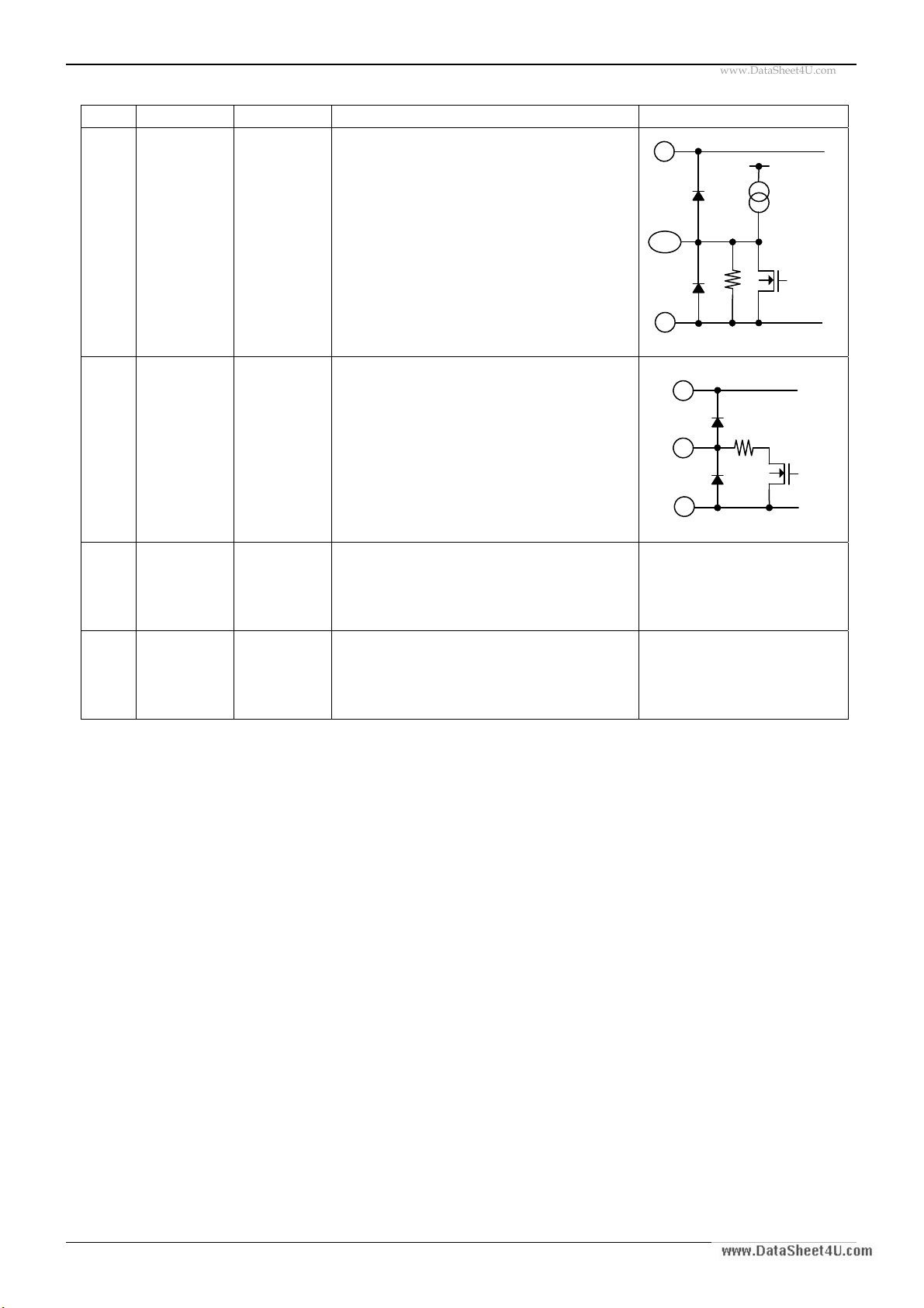
No. Pin name Pin voltage Pin explanation Internal equivalence circuit
53,54
28,29
Internal power supply pin for ch1 Gate driver
1
27
REG_G1
REG_G2
5.5V
Internal power supply pin for ch2 Gate driver
1
27
Please connect the capacitor.
45,46
36,37
25
Bias pin for PWM signal
2
FILP 1.75V~2.55V
2
Please connect the capacitor.
6
25
550K
3
4
PLMT 0V Power limiter setting terminal
Bias pin for Analog signal
FILA 2.5V
Please connect the capacitor.
3
400K
6
27
50K
4
50K
6
25
Internal power supply pin for Digital circuit
5
REG3 3.3V
Please connect the capacitor.
6
GNDA 0V GND pin for Analog signal -
5
500K
6
www.rohm.com
© 2010 ROHM Co., Ltd. All rights reserved.
7/30
2010.05 - Rev.B
Page 8
BD5446EFV
www.DataSheet4U.com
Technical Note
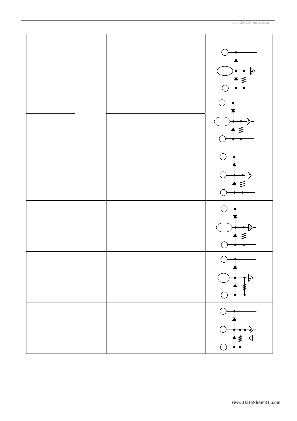
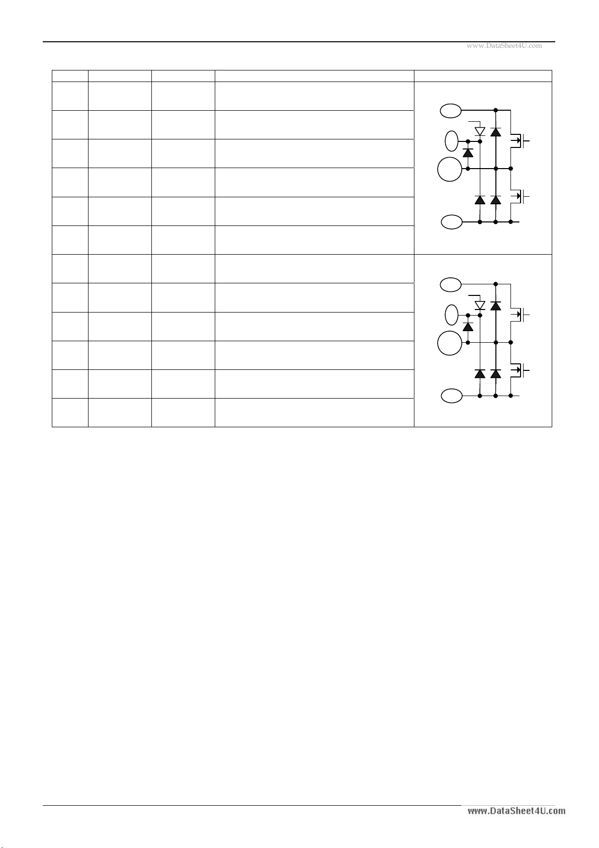
No. Pin name Pin voltage Pin explanation Internal equivalence circuit
7
8
9
10
11
SYS_CLK
BCLK
LRCLK
SDATA1
SDATA2
0V Digital audio signal input pin
5
7,8,9
10,11
6
50K
12 RESETX
13 MUTEX
14
PDX
0V
15 IIS_LJ 0V
16
17
18
GAIN1
GAIN2
GAIN3
0V
Reset pin for Digital circuit
H: Reset OFF
L: Reset ON
Speaker output mute control pin
H: Mute OFF
L: Mute ON
Power down control pin
H: Power down OFF
L: Power down ON
Digital audio signal data format setting terminal
H: Left Justified format
2
S format
L: I
Gain setting terminal
Gain=20dB~34dB, 2dB step
5
12,13,14
6
5
15
6
5
16,17,18
50K
50K
50K
19
20
TEST1
TEST2
21 SEL_DAC 0V
0V
Test pin
Please connect to GND.
DAC output selection terminal
H: SDATA2 is output from the DAC
L: SDATA1 is output from the DAC
6
5
19,20
50K
6
5
21
50K
6
www.rohm.com
© 2010 ROHM Co., Ltd. All rights reserved.
8/30
2010.05 - Rev.B
Page 9
BD5446EFV
www.DataSheet4U.com
Technical Note
No. Pin name Pin voltage Pin explanation Internal equivalence circuit
25
ch2 DAC output pin
22
23
OUT_DAC2
OUT_DAC1
2.5V
ch1 DAC output pin
Please connect it with the latter part circuit
through the capacitor.
22,23
50K
6
25
24 ERROR 3.3V
25 VCCA VCC
26,30
34,35
41,47
N.C. -
48,52
Error flag pin
Please connect pull-up resistor.
H: While Normal
L: While Error
Power supply pin for Analog signal
Non connection pin
24
500
6
-
-
www.rohm.com
© 2010 ROHM Co., Ltd. All rights reserved.
9/30
2010.05 - Rev.B
Page 10
BD5446EFV
www.DataSheet4U.com
Technical Note
No. Pin name Pin voltage Pin explanation Internal equivalence circuit
28,29 VCCP2 Vcc Power supply pin for ch2 PWM signal
31,32 OUT2P Vcc~0V
33
BSP2P
-
Output pin of ch2 positive PWM
Please connect to Output LPF.
Boot-strap pin of ch2 positive
Please connect the capacitor.
36,37 GNDP2 0V GND pin for ch2 PWM signal
28,29
33
40
31,32
38,39
38,39 OUT2N Vcc~0V
40 BSP2N -
42 BSP1N -
43,44 OUT1N Vcc~0V
Output pin of ch2 negative PWM
Please connect to Output LPF.
Boot-strap pin of ch2 negative
Please connect the capacitor.
Boot-strap pin of ch1 negative
Please connect the capacitor.
Output pin of ch1 negative PWM
Please connect to Output LPF.
45,46 GNDP1 0V GND pin for ch1 PWM signal
49 BSP1P -
50,51 OUT1P Vcc~0V
Boot-strap pin of ch1 positive
Please connect the capacitor.
Output pin of ch1 positive PWM
Please connect to Output LPF.
36,37
53,54
42
49
43,44
50,51
45,46
53,54 VCCP1 - Power supply pin for ch1 PWM signal
www.rohm.com
© 2010 ROHM Co., Ltd. All rights reserved.
10/30
2010.05 - Rev.B
Page 11

BD5446EFV
www.DataSheet4U.com
●GAIN1 pin, GAIN2 pin, GAIN3 pin function
GAIN3
(18pin)
L L L 20dB
L L H 22dB
L H L 24dB
L H H 26dB
H L L 28dB
H L H 30dB
H H L 32dB
H H H 34dB
●SEL_DAC pin function
SEL_DAC
(21pin)
L The Lch signal of SDATA1 is output The Rch signal of SDATA1 is output
H The Lch signal of SDATA2 is output The Rch signal of SDATA2 is output
●RESETX pin function
RESETX
(10pin)
L Reset ON
H Reset OFF
●RESETX pin
RESETX
(12pin)
L Reset ON
H Reset OFF
●PDX pin,MUTEX pin function
PDX
(12pin)
L L or H ON HiZ_Low
H L
H H Normal operation
●IIS_LJ pin function
IIS_LJ
(15pin)
L I2S
H Left Justified
GAIN2
(17pin)
MUTEX
(11pin)
GAIN1
(16pin)
OUT_DAC1 (23pin) OUT_DAC2 (24pin)
State of Digital block
State of Digital block
Power Down
OFF Normal operation
Digital data format
Speaker output gain
DAC output
(24,25pin)
Technical Note
PWM output
(33,34,38,39,43,44,48pin)
HiZ_Low
www.rohm.com
© 2010 ROHM Co., Ltd. All rights reserved.
11/30
2010.05 - Rev.B
Page 12

BD5446EFV
www.DataSheet4U.com
Technical Note
●Input digital audio signal sampling frequency (fs) explanation
PWM sampling frequency, Soft-start, Soft-mute time, and the detection time of the DC voltage protection in the speaker
depends on sampling frequency (fs) of the digital audio input.
Sampling frequency of the
digital audio input
(fs)
PWM sampling frequency
(fpwm)
Soft-start / Soft-mute time
DC voltage protection in
the speaker detection time
32kHz 512kHz 64msec. 64msec.
44.1kHz 705.6kHz 46msec. 46msec.
48kHz 768kHz 43msec. 43msec.
●For voltage gain (Gain setting)
BD5446EFV prescribe voltage gain at speaker output (BTL output) under the definition 0dBV (1Vrms) as full scale input of
the digital audio input signal. For example, digital audio input signal = Full scale input, Gain setting = 20dB, Load resistance
= 8Ω will give speaker output (BTL output) amplitude as Vo=10Vrms. (Output power Po = Vo2/R
R
L_SP
= 12.5W )
L_SP
●Speaker output and DAC output
Digital audio input signal SDATA1 will be output to the speaker. (SDATA2 will not be output to the speaker. DAC output can
be selected either from digital audio input signal SDATA1 or SDATA2.)
●Format of digital audio input
・SYS_CLK: It is System Clock input signal.
It will input LRCLK, BCLK, SDATA1 (SDATA2) that synchronizes with this clock that are 256 times of sampling frequency
(256fs).
・LRCLK: It is L/R clock input signal.
It corresponds to 32kHz/44.1kHz/48kHz with those clock (fs) that are same to the sampling frequency (fs) .
The data of a left channel and a right channel for one sample is input to this section.
・BCLK: It is Bit Clock input signal.
It is used for the latch of data in every one bit by sampling frequency’s 64 times sampling frequency (64fs).
・SDATA1 & SDATA2: It is Data input signal.
It is amplitude data. The data length is different according to the resolution of the input digital audio data.
It corresponds to 16/ 20/ 24 bit.
www.rohm.com
© 2010 ROHM Co., Ltd. All rights reserved.
12/30
2010.05 - Rev.B
Page 13

BD5446EFV
www.DataSheet4U.com
●I2S data format
LRCLK
BCLK
SDATA1
(SDATA2)
1/64fs
MSB
22 21 20 19 18 17 16 15 14
Lch
1
LSB
10 9
8 13 12 11
3
54
2
6
MSB
22 21 20 19 18 17 16 15 1413 12 11
32 clocks
Fig.20 I2S Data Format 64fs, 24 bit Data
LRCLK
BCLK
SDATA1
(SDATA2)
MSB
18 17 9 8 7 6 5
Lch
LSB
4321
Fig.21 I2S Data Format 64fs, 20 bit Data
MSB
18 1716 15 14 13 1 2 11 10
16 15 14 13 12 11 10 9 8 7 6 5 4 3 2 1
LRCLK
BCLK
SDATA1
(SDATA2)
MSB MSB
9876514 13 12 11 10
Lch
4321
LSB
Fig.22 I2S Data Format 64fs, 16 bit Data
The Low section of LRCLK becomes Lch, the High section of LRCLK becomes Rch.
After changing LRCLK, second bit becomes MSB.
●Left-justified format
LRCLK
BCLK
SDATA1
(SDATA2)
MSB
22 21 20 19 18 17 16 15 14
Lch1/64fs
10 9
32 clocks
8
3
2
6
LSB
1
54
MSB
22 21 20 19 18 17 16 15 1413 12 11
Fig.23 Left-Justified Data Format 64fs, 24 bit Data
LRCLK
BCLK
SDATA1
(SDATA2)
MSB
18 17 9 8 7 6 5
Lch
4321
LSB
MSB
18 1716 15 14 13 12 11 1 0
16 15 14 13 12 11 10 9 8 7 6 5 4 3 2 1
Fig.24 Left-Justified Data Format 64fs, 20 bit Data
LRCLK
Lch
BCLK
SDATA1
(SDATA2)
MSB MSB
9876514 13 12 11 10
4321
LSB
Fig.25 Left-Justified Data Format 64fs, 16 bit Data
9876514 13 12 11 10
The High section of LRCLK becomes Lch, the Low section of LRCLK becomes Rch.
After changing LRCLK, first bit becomes MSB.
Technical Note
Rch
10 9
87
76
54
32 clocks
Rch
Rch
9876514 13 12 11 10
4321
LSB
Rch
10 9
6
13 12 11
87
354 12
7
32 clocks
Rch
LSB
Rch
LSB
4321
LSB
3
12
LSB
LSB
www.rohm.com
© 2010 ROHM Co., Ltd. All rights reserved.
13/30
2010.05 - Rev.B
Page 14

BD5446EFV
www.DataSheet4U.com
●Power supply start-up sequence
VCCA (25pin)
VCCP1 (53, 54pin)
VCCP2 (28, 29pin)
①Power up VCCA, VCCP1, VCCP2 simultaneously.
REG_3 (5pin)
REG_G1 (1pin)
REG_G2 (27pin)
Technical Note
t
REG_G1, REG_G2
REG_3
t
RESETX (12pin)
SYS_CLK (7pin)
BCLK (8pin)
LRCLK (9pin)
SDATA1 (10pin)
SDATA2 (11pin)
PDX (14pin)
OUT_DAC1 (23pin)
OUT_DAC2 (22pin)
MUTEX (13pin)
②Set RESETX to High after power up.
t
③Degital audio data communication.
t
④Set PDX to High.
t
t
www.rohm.com
© 2010 ROHM Co., Ltd. All rights reserved.
Speaker output
⑤Set MUTEX to High.
Soft-start
43msec(fs=48kH z)
14/30
t
t
2010.05 - Rev.B
Page 15

BD5446EFV
www.DataSheet4U.com
●Power supply shut-down sequence
VCCA (25pin)
VCCP1 (53, 54pin)
VCCP2 (28, 29pin)
Technical Note
⑤Power down VCCA, VCCP1, VCCP2, simultaneously.
t
REG_3 (5pin)
REG_G1 (1pin)
REG_G2 (27pin)
RESETX (12pin)
SYS_CLK (7pin)
BCLK (8pin)
LRCLK (9pin)
SDATA1 (10pin)
SDATA2 (11pin)
PDX (14pin)
OUT_DAC1 (23pin)
OUT_DAC2 (22pin)
REG_G1, REG_G2
REG_3
④Set RESETX to Low
③Stop digital audio date signal.
②Set PDX to Low.
t
t
t
t
MUTEX (13pin)
①Set MUTEX to Low.
Soft-mute
43msec(fs=48kHz)
t
t
t
www.rohm.com
© 2010 ROHM Co., Ltd. All rights reserved.
15/30
2010.05 - Rev.B
Page 16

BD5446EFV
www.DataSheet4U.com
●About the protection function
Technical Note
Protection function Detecting & Releasing condition
Output short
protection
DC voltage protection
in the speaker
High temperature
protection
Under voltage
protection
Detecting
condition
Detecting
condition
Detecting
condition
Releasing
condition
Detecting
condition
Releasing
condition
Detecting
condition
Detecting current = 10A (TYP.)
PWM output Duty=0% or 100%
43msec(fs=48kHz) above fixed
Chip temperature to be above 150℃ (TYP.)
Chip temperature to be below 120℃ (TYP.)
Power supply voltage to be below 8V (TYP.)
Power supply voltage to be above 9V (TYP.)
No change to SYS_CLK more than 1usec (TYP.)
Clock stop protection
Releasing
condition
* The ERROR pin is Nch open-drain output.
* Once an IC is latched, the circuit is not released automatically even after an abnormal status is removed.
The following procedures ① or ② is available for recovery.
①After the MUTEX pin is made Low once, the MUTEX pin is returned to High again.
②Turning on the power supply again.
Normal input to SYS_CLK
DAC
Output
Normal
operation
Normal
operation
Normal
operation
Irregular
output
Normal
operation
PWM
Output
ERROR
Output
HiZ_Low
(Latch) L (Latch)
HiZ_Low
(Latch) L (Latch)
HiZ_Low
Normal
operation
HiZ_Low
Normal
operation
HiZ_Low
Normal
operation
H
H
H
www.rohm.com
© 2010 ROHM Co., Ltd. All rights reserved.
16/30
2010.05 - Rev.B
Page 17

BD5446EFV
www.DataSheet4U.com
Technical Note
1) High temperature protection
This IC has the high temperature protection circuit that prevents thermal reckless driving under an abnormal state for the
temperature of the chip to exceed Tjmax=150℃.
Detecting condition - It will detect when MUTE pin is set High and the temperature of the chip becomes 150℃(TYP.) or
more. The speaker output is muted through a soft-mute when detected.
Releasing condition - It will release when MUTE pin is set High and the temperature of the chip becomes 120℃(TYP.)
or less. The speaker output is outputted through a soft-start when released.
Temperature of
IC chip junction(℃)
150℃
120℃
OUT1P (50, 51pin)
OUT1N (43, 44pin)
OUT2P (31, 32pin)
OUT2N (38, 39pin)
HiZ-Low
Speaker output
Soft-mute
43msec(fs=48KHz)
Soft-start
43msec(fs=48KHz)
t
t
ERROR (24pin)
OUT_DAC1 (23pin)
OUT_DAC2 (22pin)
t
3.3V
t
t
www.rohm.com
© 2010 ROHM Co., Ltd. All rights reserved.
17/30
2010.05 - Rev.B
Page 18

BD5446EFV
www.DataSheet4U.com
Technical Note
2) Under voltage protection
This IC has the under voltage protection circuit that make speaker output mute once detecting extreme drop of the power
supply voltage.
Detecting condition – It will detect when MUTE pin is set High and the power supply voltage becomes lower than 8V.
The speaker output is muted through a soft-mute when detected.
Releasing condition – It will release when MUTE pin is set High and the power supply voltage becomes more than 9V.
The speaker output is outputted through a soft-start when released.
VCCA (25pin)
VCCP1 (53, 54pin)
VCCP2 (28, 29pin)
OUT1P (50, 51pin)
OUT1N (43, 44pin)
OUT2P (31, 32pin)
OUT2N (38, 39pin)
8V
HiZ-Low
9V
t
t
Speaker output
ERROR (24pin)
OUT_DAC1 (23pin)
OUT_DAC2 (22pin)
Soft-mute
43msec(fs=48kHz)
3.3V
Soft-start
43msec(fs=48kHz)
t
t
t
www.rohm.com
© 2010 ROHM Co., Ltd. All rights reserved.
18/30
2010.05 - Rev.B
Page 19

BD5446EFV
www.DataSheet4U.com
Technical Note
3) Clock stop protection
This IC has the clock stop protection circuit that make the speaker output mute when the SYS_CLK signal of the digital
audio input stops.
Detecting condition - It will detect when MUTE pin is set High and the SYS_CLK signal stops for about 1usec or more.
The speaker output is muted through a soft-mute when detected.
Releasing condition - It will release when MUTE pin is set High and the SYS_CLK signal returns to the normal clock
operation. The speaker output is outputted through a soft-start when released.
Clock stop Clock recover
SYS_CLK (7pin)
Protection start with
about 1μsec clock stop.
OUT1P (50, 51pin)
OUT1N (43, 44pin)
OUT2P (31, 32pin)
OUT2N (38, 39pin)
HiZ-Low
t
t
Speaker output
ERROR (24pin)
OUT_DAC1 (23pin)
OUT_DAC2 (22pin)
3.3V
Unstable
Soft-start
43msec(fs=48kHz)
t
t
t
www.rohm.com
© 2010 ROHM Co., Ltd. All rights reserved.
19/30
2010.05 - Rev.B
Page 20

BD5446EFV
www.DataSheet4U.com
Technical Note
4)Output short protection(Short to the power supply)
This IC has the PWM output short protection circuit that stops the PWM output when the PWM output is short-circuited to
the power supply due to abnormality.
Detecting condition - It will detect when MUTE pin is set High and the current that flows in the PWM output pin
becomes 10A(TYP.) or more. The PWM output instantaneously enters the state of HiZ-Low if
detected, and IC does the latch.
Releasing method - ①After the MUTEX pin is set Low once, the MUTEX pin is set High again.
②Turning on the power supply again.
Short to VCC Release from short to VCC
OUT1P (50, 51pin)
OUT1N (43, 44pin)
OUT2P (31, 32pin)
OUT2N (38, 39pin)
Over current
10A(TYP.)
PWM out : IC latches with HiZ-Low.
Released from latch state.
ERROR (24pin)
t
t
MUTEX(13pin)
1μsec(TYP.)
t
Latch release
t
5) Output short protection(Short to GND)
This IC has the PWM output short protection circuit that stops the PWM output when the PWM output is short-circuited to
GND due to abnormality.
Detecting condition - It will detect when MUTE pin is set High and the current that flows in the PWM output terminal
becomes 10A(TYP.) or more. The PWM output instantaneously enters the state of HiZ-Low if
detected, and IC does the latch.
Releasing method – ①After the MUTEX pin is set Low once, the MUTEX pin is set High again.
②Turning on the power supply again.
Short to GND
Release from short to
GND
OUT1P (50, 51pin)
OUT1N (43, 44pin)
OUT2P (31, 32pin)
OUT2N (38, 39pin)
www.rohm.com
© 2010 ROHM Co., Ltd. All rights reserved.
Over current
ERROR (24pin)
MUTEX(13pin)
10A(TYP.)
1μsec(TYP.)
PWM out : IC latches with HiZ-Low.
20/30
Released from latch state.
Latch release
t
t
t
t
2010.05 - Rev.B
Page 21

BD5446EFV
www.DataSheet4U.com
Technical Note
6) DC voltage protection in the speaker
When the DC voltage in the speaker is impressed due to abnormality, this IC has the protection circuit where the speaker
is defended from destruction.
Detecting condition - It will detect when MUTE pin is set High or Low and PWM output Duty=0% or 100% ,
43msec(fs=48kHz) or above. Once detected, The PWM output instantaneously enters the state
of HiZ-Low, and IC does the latch.
Releasing method – ①After the MUTEX pin is set Low once, the MUTEX pin is set High again.
②Turning on the power supply again
PWM out locked duty=100% abnormal state.
Abnormal state release.
OUT1P (50, 51pin)
OUT1N (43, 44pin)
OUT2P (31, 32pin)
OUT2N (38, 39pin)
Speaker output
PWM output : IC latche with HiZ-Low.
Latch release state.
ERROR (24pin)
Protection start surge current
into speaker output for 43msec
(fs=48kHz) and over.
Soft-start
43msec(fs=48kHz)
t
t
MUTEX(13pin)
t
Latch release
t
www.rohm.com
© 2010 ROHM Co., Ltd. All rights reserved.
21/30
2010.05 - Rev.B
Page 22

BD5446EFV
– 3p
www.DataSheet4U.com
Technical Note
●Output power limiter function
This IC is provided with an output power limiter function to protect speakers from destruction by an excessive output.
Limiter values are freely specified by changing external resistors R1/R2 as shown in Fig-26. Fig-27 shows a speaker output
waveform that is generated with use of the output limiter function. Because the waveform is soft-clipped, unusual noises on
audible signals are significantly reduced under operation of limiter.
Use resistors with a high degree of accuracy for R1 and R2 (±1% or higher accuracy is recommended). The capacitor C is
for the noise removal of output power limitation terminal (3pin). Provide grounding with a 1µF capacitor. Specify a resistor of
10kΩ or higher resistor R1 and R2. If the output power limiter function is not used, R1, R2 and C is unnecessary. However,
connect 3pin with GNDA.
Power
Limiter
3
REG_3
5
Speaker
output
R1
R2
C
1μF
5pin
3.3V
Soft Clip
1μF
Fig-27
GNDA
Fig-26
10
9
8
7
6
5
4
3
VCC=13V, RL=8Ω, f=1kHz
2
Gain=20dB, 5pin=3.3V
OUTPUT POWER(W/ch) .
1
0
1 1.2 1.4 1.6 1 .8 2
3pin terminal vol tage [V]
www.rohm.com
© 2010 ROHM Co., Ltd. All rights reserved.
Fig.28
Output power
in terminal voltage
22/30
2010.05 - Rev.B
Page 23

BD5446EFV
www.DataSheet4U.com
Technical Note
●Application Circuit Example(R
Digital Audio
Source
μ-con
GNDP1
GNDA
SYS_CLK (256fs)
BCLK (64fs)
LRCLK
SDATA1
SDATA2
RESETX
MUTEX
PDX
3.3V
C1
3.3μF
C2
1μF
( )
( )
C4
1μF
C5
1μF
(fs=32kHz~48kHz)
1
2
3
( )
4
5
6
7
8
9
10
11
12
13
14
15
16
17
C25D
C27
C22
C23
R24
3.3V
18
19
20
21
22
23
24
25
26
NC
27
REG_G2
VSS
VSS
OUT_DAC2
(Rch)
OUT_DAC1
(Lch)
ERROR
VCCA
GNDA
GNDA
GNDP2
C25
0.1μF
10μF
1μF
1μF
100kΩ
3.3μF
L_SP
REG_G1
FILP
Power
Limiter
FILA
REG_3
GNDA
I2S/LJ
Interface
Control
Interface
I2S/LJ
Selector
Gain
Selector
TEST
DAC
Selector
DAC
VCCA
=8Ω)
×8 Over
Sampling
Digital
Filter
PWM
Modulator
High Temperature Protection
Under Voltage Protection
Clock Stop Protection
Output Short Protection
Output DC Voltage Protection
Driver
1P
Driver
1N
Driver
2N
Driver
2P
VCCP1
VCCP2
REG_G1
GNDP1
REG_G1
REG_G2
GNDP2
REG_G2
NC
NC
NC
NC
NC
NC
NC
54
53
52
51
50
C49
1μF
49
48
C53 C53D
1μF
47
46
45
44
43
42
41
40
39
38
37
36
35
1μF
C28
34
33
1μF
C31
32
31
30
29
28
VCCP1
GNDP1
C42
1μF
1μF
C38
GNDP2
VCCP2
220μF
220μF
C28D
470pF
C50B
5.6Ω
R50B
R43B
5.6Ω
C43B
470pF
470pF
C38B
5.6Ω
R38B
R31B
5.6Ω
C31B
470pF
L50
22μH
0.068μF
GNDP1
0.068μF
22μH
L43
L38
22μH
0.068μF
GNDP2
0.068μF
22μH
L31
C50A
C43A
C38A
C31A
0.33μF
C43C
0.33μF
C31C
8Ω
Lch
(SDATA1)
8Ω
Rch
(SDATA1)
www.rohm.com
© 2010 ROHM Co., Ltd. All rights reserved.
23/30
2010.05 - Rev.B
Page 24

BD5446EFV
www.DataSheet4U.com
Technical Note
●BOM list(R
Parts Parts No. Value Company Product No.
IC U1 - ROHM BD5446EFV - - 18.5mm×9.5mm
Inductor L31, L38, L43, L50 22μH
Resistor
Capacitor
=8Ω)
L_SP
TOKO 1168ER-0001
SAGAMI DBE7210H-220M - (±20%) 10.5mm×6.4mm
R31B, R38B
R43B, R50B
C31, C38, C42, C49 1μF
C25, C28, C53 0.1μF GRM188B31H104KA92 50V B(±10%) 1.6mm×0.8mm
C31A, C38A
C43A, C50A
C31C, C43C 0.33μF GRM219B31H334KA87 50V B(±10%) 2.0mm×1.25mm
C1, C27 3.3μF GRM188B31A335KE15 10V B(±10%) 1.6mm×0.8mm
5.6Ω ROHM MCR18PZHZFL5R60 1/4W F(±1%) 3.2mm×1.6mm
GRM185B31C105KE43 16V B(±10%
0.068μF GRM21BB11H683KA01 50V B(±10%
MURATA
Rated
Voltage
Tolerance Size
- (±20%) 10.3mm×7.6mm
) 1.6mm×0.8mm
) 2.0mm×1.25mm
Electrolytic
Capacitor
C2, C4, C5
C22, C23
C31B, C38B
C43B, C50B
C28D, C53D 220μF
C25D 10μF EEUFC1H100L 50V ±20% φ5mm×11mm
1μF GRM185B30J105KE25 6.3V B(±10%
470pF GRM188B11H471KA 50V B(±10%
ECA1VMH221 35V ±20% φ8mm×11.5mm
Panasonic
) 1.6mm×0.8mm
) 2.0mm×1.2mm
www.rohm.com
© 2010 ROHM Co., Ltd. All rights reserved.
24/30
2010.05 - Rev.B
Page 25

BD5446EFV
www.DataSheet4U.com
Technical Note
●Application Circuit Example(R
Digital Audio
Source
μ-con
GNDP1
GNDA
SYS_CLK (256fs)
BCLK (64fs)
LRCLK
SDATA1
SDATA2
RESETX
MUTEX
PDX
3.3V
C1
3.3μF
C2
1μF
( )
( )
C4
1μF
C5
1μF
(fs=32kHz~48kHz)
1
2
3
( )
4
5
6
7
8
9
10
11
12
13
14
15
16
17
18
19
1μF
1μF
C25D
C27
C22
C23
R24
3.3V
20
21
22
23
24
25
26
NC
27
C25
0.1μF
10μF
VSS
100kΩ
3.3μF
VSS
OUT_DAC2
(Rch)
OUT_DAC1
(Lch)
ERROR
VCCA
GNDA
GNDA
GNDP2
L_SP
Power
Limiter
I2S/LJ
Interface
Control
Interface
I2S/LJ
Selector
Gain
Selector
TEST
DAC
Selector
DAC
VCCA
REG_G2
REG_G1
FILP
FILA
REG_3
GNDA
=6Ω)
×8 Over
Sampling
Digital
Filter
PWM
Modulator
High Temperature Protection
Under Voltage Protection
Clock Stop Protection
Output Short Protection
Output DC Voltage Protection
Driver
1P
Driver
1N
Driver
2N
Driver
2P
VCCP1
VCCP2
REG_G1
GNDP1
REG_G1
REG_G2
GNDP2
REG_G2
NC
NC
NC
NC
NC
NC
NC
54
53
52
51
50
C49
1μF
49
48
C53 C53D
1μF
47
46
45
44
43
42
41
40
39
38
37
36
35
1μF
C28
34
33
1μF
C31
32
31
30
29
28
VCCP1
GNDP1
C42
1μF
1μF
C38
GNDP2
VCCP2
220μF
220μF
C28D
470pF
C50B
5.6Ω
R50B
R43B
5.6Ω
C43B
470pF
470pF
C38B
5.6Ω
R38B
R31B
5.6Ω
C31B
470pF
L50
15μH
0.1μF
GNDP1
0.1μF
15μH
L43
L38
15μH
GNDP2
15μH
L31
0.1μF
0.1μF
C50A
C43A
C38A
C31A
0.47μF
C43C
0.47μF
C31C
6Ω
Lch
(SDATA1)
6Ω
Rch
(SDATA1)
www.rohm.com
© 2010 ROHM Co., Ltd. All rights reserved.
25/30
2010.05 - Rev.B
Page 26

BD5446EFV
www.DataSheet4U.com
Technical Note
●BOM list(R
Parts Parts No. Value Company Product No.
IC U1 - ROHM BD5446EFV - - 18.5mm×9.5mm
Inductor L31, L38, L43, L50 15μH SAGAMI DBE7210H-150M - (±20%) 10.5mm×6.4mm
Resistor
Capacitor
=6Ω)
L_SP
R31B, R38B
R43B, R50B
C31, C38, C42, C49 1µF
C25, C28, C53, C31A,
C38A, C43A, C48A
C31C, C43C 0.47μF GRM21BB31H474KA87 50V B(±10%) 2.0mm×1.2mm
C1, C27 3.3μF GRM188B31A335KE15 10V B(±10%) 1.6mm×0.8mm
C2, C4, C5
C22, C23
C31B, C38B
C43B, C50B
Rated
Voltage
5.6Ω ROHM MCR18PZHZFL5R60 1/4W F(±1%) 3.2mm×1.6mm
GRM185B31C105KE43 16V B(±10%
0.1μF GRM188B31H104KA92 50V B(±10%
MURATA
1μF GRM185B30J105KE25 6.3V B(±10%
470pF GRM188B11H471KA 50V B(±10%
Tolerance Size
) 1.6mm×0.8mm
) 1.6mm×0.8mm
) 1.6mm×0.8mm
) 2.0mm×1.2mm
Electrolytic
Capacitor
C28D, C53D 220μF
Panasonic
C25D 10μF EEUFC1H100L 50V ±20% φ5mm×11mm
ECA1VMH221 35V ±20% φ8mm×11.5mm
www.rohm.com
© 2010 ROHM Co., Ltd. All rights reserved.
26/30
2010.05 - Rev.B
Page 27

BD5446EFV
ro r
f
www.DataSheet4U.com
Technical Note
●Output LC Filter Circuit
An output filter is required to eliminate radio-frequency components exceeding the audio-frequency region supplied to a
load (speaker). Because this IC uses sampling clock frequencies from 200kHz to 400kHz in the output PWM signals, the
high-frequency components must be appropriately removed.
This section takes an example of an LC type LPF shown in Fig.29, in which coil L and capacitor C compose a differential
filter with an attenuation property of -12dB/oct. A large part of switching currents flow to capacitor C, and only a small part
of the currents flow to speaker R
. This filter reduces unwanted emission this way. In addition, coil L and capacitor Cg
L
compose a filter against in-phase components, reducing unwanted emission further.
Filter constants depend on load impedances. The following are formulas to calculate values of L, C, and Cg when Q=0.707
is specified.
4 8 , 4 9
o
3 8 , 3 9
4 5 , 4 6
3 3 , 3 4
L
g
C
C
Cg
L
R
L
Cg = 0 . 2 C F
L =
C =
RL2
H
4 π
C
1
2 π f C R L2
F
Fig. 29
R
: Load impedance (Ω)
L
: LPF cut off frequency (Hz)
f
C
Following presents output LC filter constants with typical load impedances.
fC = 30kHz fC = 40kHz
L C Cg RL L C Cg
R
L
6Ω 22µH 0.68µF 0.15µF 6Ω 15µH 0.47µF 0.1µF
8Ω 33µH 0.47µF 0.1µF 8Ω 22µH 0.33µF 0.068µF
16Ω 68µH 0.22µF 0.047µF 16Ω 47µH 0.15µF 0.033µF
Use coils with a low direct-current resistance and with a sufficient margin of allowable currents. A high direct-current
resistance causes power losses. In addition, select a closed magnetic circuit type product in normal cases to prevent
unwanted emission.
Use capacitors with a low equivalent series resistance, and good impedance characteristics at high frequency ranges
(100kHz or higher). Also, select an item with sufficient withstand voltage because flowing massive amount of
high-frequency currents is expected.
www.rohm.com
© 2010 ROHM Co., Ltd. All rights reserved.
27/30
2010.05 - Rev.B
Page 28

BD5446EFV
www.DataSheet4U.com
●Notes for use
1 ) Absolute maximum ratings
Use of the IC in excess of absolute maximum ratings such as the applied voltage or operating temperature range may
result in IC damage. Assumptions should not be made regarding the state of the IC (short mode or open mode) when
such damage is suffered. A physical safety measure such as a fuse should be implemented when use of the IC in a
special mode where the absolute maximum ratings may be exceeded is anticipated.
2 ) Power supply lines
As return of current regenerated by back EMF of output coil happens, take steps such as putting capacitor between
power supply and GND as a electric pathway for the regenerated current. Be sure that there is no problem with each
property such as emptied capacity at lower temperature regarding electrolytic capacitor to decide capacity value. If the
connected power supply does not have sufficient current absorption capacity, regenerative current will cause the voltage
on the power supply line to rise, which combined with the product and its peripheral circuitry may exceed the absolute
maximum ratings. It is recommended to implement a physical safety measure such as the insertion of a voltage clamp
diode between the power supply and GND pins.
3 ) GND potential(Pin 6, 36, 37, 45, 46).
Any state must become the lowest voltage about GND terminal and VSS terminal.
4 ) Input terminal
The parasitic elements are formed in the IC because of the voltage relation. The parasitic element operating causes the
wrong operation and destruction. Therefore, please be careful so as not to operate the parasitic elements by impressing
to input terminals lower voltage than GND and VSS. Please do not apply the voltage to the input terminal when the
power-supply voltage is not impressed.
5 ) Setting of heat
Use a thermal design that allows for a sufficient margin in light of the power dissipation (Pd) in actual operating conditions.
This IC exposes its frame of the backside of package. Note that this part is assumed to use after providing heat
dissipation treatment to improve heat dissipation efficiency. Try to occupy as wide as possible with heat dissipation
pattern not only on the board surface but also the backside.
Class D speaker amplifier is high efficiency and low heat generation by comparison with conventional Analog power
amplifier. However, In case it is operated continuously by maximum output power, Power dissipation (Pdiss) may exceed
package dissipation. Please consider about heat design that Power dissipation (Pdiss) does not exceed Package
dissipation (Pd) in average power (Poav). (Tjmax : Maximum junction temperature=150℃, Ta : Peripheral temperature[℃],
θja : Thermal resistance of package[℃/W], Poav : Average power[W], η : Efficiency)
Package dissipation : Pd(W)=(Tjmax - Ta)/θja
Power dissipation : Pdiss(W)= Poav ×(1/η- 1)
6 ) Actions in strong magnetic field
Use caution when using the IC in the presence of a strong magnetic field as doing so may cause the IC to malfunction.
Technical Note
7 ) Thermal shutdown circuit
This product is provided with a built-in thermal shutdown circuit. When the thermal shutdown circuit operates, the output
transistors are placed under open status. The thermal shutdown circuit is primarily intended to shut down the IC avoiding
thermal runaway under abnormal conditions with a chip temperature exceeding Tjmax = 150℃.
8 ) Shorts between pins and misinstallation
When mounting the IC on a board, pay adequate attention to orientation and placement discrepancies of the IC. If it is
misinstalled and the power is turned on, the IC may be damaged. It also may be damaged if it is shorted by a foreign
substance coming between pins of the IC or between a pin and a power supply or a pin and a GND.
9 ) Power supply on/off (Pin 25, 28, 29, 53, 54)
In case power supply is started up, RESETX(Pin 12), MUTEX(Pin 13) and PDX (Pin 14) always should be set Low. And
in case power supply is shut down, it should be set Low likewise. Then it is possible to eliminate pop noise when power
supply is turned on/off. And also, all power supply terminals should start up and shut down together.
10 ) ERROR terminal(Pin 24)
error flag is outputted when Output short protection and DC voltage protection in the speaker are operated. These flags
A
are the function which the condition of this product is shown in.
11 ) N.C. terminal(Pin 26, 30, 34, 35, 41, 47, 48, 52)
N.C. terminal (Non Connection Pin) does not connect to the inside circuit. Therefore, possible to use open.
12 ) TEST terminal(Pin 19, 20)
TEST terminal connects with ground to prevent the malfunction by external noise.
13 ) Precautions for Spealer-setting
If the impedance characteristics of the speakers at high-frequency range while increase rapidly, the IC might not have
stable-operation in the resonance frequency range of the LC-filter. Therefore, consider adding damping-circuit, etc.,
depending on the impedance of the speaker.
www.rohm.com
© 2010 ROHM Co., Ltd. All rights reserved.
28/30
2010.05 - Rev.B
Page 29

BD5446EFV
www.DataSheet4U.com
●Allowable Power Dissipation
7
6
5
4
3
2
Power Diss ipation Pd (W)
1
0
0 10 20 30 40 50 60 70 80 90 100 110 120 130 140 150
Measuring instrument : TH-156(Shibukawa Kuwano Electrical Instruments Co., Ltd.)
Measuring conditions : Installation on ROHM’s board
Board size : 70mm×70mm×1.6mm(with thermal via on board)
Material : FR4
・The board on exposed heat sink on the back of package are connected by soldering.
PCB① : 1-layer board(back copper foil size: 0mm×0mm), θja=62.5℃/W
PCB② : 2-layer board(back copper foil size: 70mm×70mm),θja=27.8℃/W
PCB③ : 4-layer board(back copper foil size: 70mm×70mm),θja=20.2℃/W
Technical Note
PCB③ 6.2W
PCB② 4.5W
PCB① 2.0W
Ambient Temperature:Ta(℃)
www.rohm.com
© 2010 ROHM Co., Ltd. All rights reserved.
29/30
2010.05 - Rev.B
Page 30

BD5446EFV
www.DataSheet4U.com
●Ordering part number
Technical Note
B D 5 4 4 6 E F V - E 2
Part No. Part No.
HTSSOP-B54
(MAX 18.85 include BURR)
54 28
9.5±0.2
7.5±0.1
1PIN MARK
0.8
1.0MAX
0.85±0.05
0.65
0.08±0.05
18.5±0.1
(6.0)
0.22
+0.05
-
0.04
+
6°
4°
−
4°
(5.0)
0.5±0.15
271
0.08
0.08
S
S
M
+0.05
0.17
-
0.03
(Unit : mm)
Package
EFV : HTSSOP-B54
<Tape and Reel information>
Embossed carrier tape (with dry pack)Tape
Quantity
Direction
of feed
1.0±0.2
1500pcs
E2
The direction is the 1pin of product is at the upper left when you hold
()
reel on the left hand and you pull out the tape on the right hand
Reel
1pin
Order quantity needs to be multiple of the minimum quantity.
∗
Packaging and forming specification
E2: Embossed tape and reel
Direction of feed
www.rohm.com
© 2010 ROHM Co., Ltd. All rights reserved.
30/30
2010.05 - Rev.B
Page 31

Notes
www.DataSheet4U.com
No copying or reproduction of this document, in par t or in whole, is permitted without the
consent of ROHM Co.,Ltd.
The content specied herein is subject to change for improvement without notice.
The content specied herein is for the purpose of introducing ROHM's products (hereinafter
"Products"). If you wish to use any such Product, please be sure to refer to the specications,
which can be obtained from ROHM upon request.
Examples of application circuits, circuit constants and any other information contained herein
illustrate the standard usage and operations of the Products. The peripheral conditions must
be taken into account when designing circuits for mass production.
Great care was taken in ensuring the accuracy of the information specied in this document.
However, should you incur any damage arising from any inaccuracy or misprint of such
information, ROHM shall bear no responsibility for such damage.
The technical information specied herein is intended only to show the typical functions of and
examples of application circuits for the Products. ROHM does not grant you, explicitly or
implicitly, any license to use or exercise intellectual property or other rights held by ROHM and
other parties. ROHM shall bear no responsibility whatsoever for any dispute arising from the
use of such technical information.
Notice
The Products specied in this document are intended to be used with general-use electronic
equipment or devices (such as audio visual equipment, ofce-automation equipment, communication devices, electronic appliances and amusement devices).
The Products specied in this document are not designed to be radiation tolerant.
While ROHM always makes efforts to enhance the quality and reliability of its Products, a
Product may fail or malfunction for a variety of reasons.
Please be sure to implement in your equipment using the Products safety measures to guard
against the possibility of physical injury, re or any other damage caused in the event of the
failure of any Product, such as derating, redundancy, re control and fail-safe designs. ROHM
shall bear no responsibility whatsoever for your use of any Product outside of the prescribed
scope or not in accordance with the instruction manual.
The Products are not designed or manufactured to be used with any equipment, device or
system which requires an extremely high level of reliability the failure or malfunction of which
may result in a direct threat to human life or create a risk of human injur y (such as a medical
instrument, transportation equipment, aerospace machinery, nuclear-reactor controller, fuelcontroller or other safety device). ROHM shall bear no responsibility in any way for use of any
of the Products for the above special purposes. If a Product is intended to be used for any
such special purpose, please contact a ROHM sales representative before purchasing.
If you intend to export or ship overseas any Product or technology specied herein that may
be controlled under the Foreign Exchange and the Foreign Trade Law, you will be required to
obtain a license or permit under the Law.
www.rohm.com
© 2010 ROHM Co., Ltd. All rights reserved.
Thank you for your accessing to ROHM product informations.
More detail product informations and catalogs are available, please contact us.
ROHM Customer Support System
http://www.rohm.com/contact/
R1010
A
 Loading...