

Page 1

Middle Power Class-D Speaker Amplifiers
Analog Input /
Single End Output
Class-D Speaker Amplifier
BD5445EFV
No.11075ECT16
●Overview
BD5445EFV is a Analog input type Class D Speaker Amplifier designed for Flat-panel TVs in particular for space-saving
and low-power consumption, delivers an output power of 17W+17W. This IC employs state-of-the-art Bipolar, CMOS, and
DMOS (BCD) process technology that eliminates turn-on resistance in the output power stage and internal loss due to line
resistances up to an ultimate level. With this technology, the IC can achieve high efficiency of 91% (10W+10W output with
8Ω load).In addition, the IC is packaged in a compact reverse heat radiation type power package to achieve low power
consumption and low heat generation and eliminates necessity of external heat-sink up to a total output power of 34W. This
product satisfies both needs for drastic downsizing, low-profile structures and powerful, high-quality playback of sound
system.
●Features
1) 17W stereo single-ended outputs
34W mono bridge-tied-load output
2) Wide supply voltage (From 10V to 27V)
3) Four selectable gain (14, 20, 26, 32dB)
4) Master / Slave function
5) Soft-start and Soft-mute
6) Low noise, Low distortion
7) Various protection functions
(High temperature, Output short, Under voltage)
8) Small power package (HTSSOP-B28)
●Applications
Flat Panel TVs (LCD, Plasma), Home Audio, Desktop PC, Amusement equipments, Electronic Music equipments, etc.
www.rohm.com
1/31
© 2011 ROHM Co., Ltd. All rights reserved.
2011.10 - Rev.C
Page 2

BD5445EFV
●Absolute maximum ratings (Ta=25℃)
Item Symbol Limit Unit Conditions
Supply voltage Vcc 30 V Pin 1, 15, 16, 27, 28 ※1 ※2
1.45 W ※3
Power dissipation Pd
3.30 W ※4
4.70 W ※5
Input voltage for signal VIN -0.3 ~ 5.3 V Pin 4, 5 ※1
Input voltage for control V
Input voltage for clock V
-0.3 ~ Vcc + 0.3 V Pin 2, 3, 10, 11, 13 ※1
CONT
-0.3 ~ 5.3 V
OSC
Pin 12 ※1
Operating temperature range Topr -25 ~ +85 ℃
Storage temperature range Tstg -55 ~ +150 ℃
Maximum junction temperature Tjmax +150 ℃
※1 The voltage that can be applied, based on Gnd(Pin6, 20, 21, 22, 23)
※2 Do not, however exceed Pd and Tjmax=150℃.
※3 70mm×70mm×1.6mm, FR4, 1-layer glass epoxy board (Copper on bottom layer 0%)
Derating in done at 11.6mW/℃ for operating above Ta=25℃.
※4 70mm×70mm×1.6mm, FR4, 2-layer glass epoxy board (Copper on bottom layer 100%)
Derating in done at 26.4mW/℃ for operating above Ta=25℃. There are thermal via on the board.
※5 70mm×70mm×1.6mm, FR4, 4-layer glass epoxy board (Copper on bottom layer 100%)
Derating in done at 37.6mW/℃ for operating above Ta=25℃. There are thermal via on the board.
●Operating conditions (Ta=25℃)
Item Symbol Limit Unit Conditions
Supply voltage Vcc 10 ~ 27 V Pin 1, 15, 16, 27, 28 ※1 ※2
Minimum load impedance RL 3.6 Ω
※6 Do not, however exceed Pd.
※ No radiation-proof design
Technical Note
※6
www.rohm.com
2/31
© 2011 ROHM Co., Ltd. All rights reserved.
2011.10 - Rev.C
Page 3
BD5445EFV
Technical Note
●Electrical characteristics ( Unless otherwise specified Ta=25℃, Vcc=24V, f=1kHz, RL=8Ω, Po=1W, Gain=20dB,
PDX=24V, MUTEX=24V, MS=0V, Single-ended outputs)
Item Symbol
Limit
Min Typ Max
Unit Conditions
Whole circuit
Circuit current 1 I
Circuit current 2
(Power down mode)
- 25 50 mA
CC1
I
- 2 4 mA
CC2
Pin 1, 15, 16, 27, 28
No load, No signal
Pin 1, 15, 16, 27, 28
PDX=0V,MUTEX=0V, No load, No
signal
Control circuit
High level input voltage for control VIH 2.5 - 24 V
Low level input voltage for control VIL 0 - 0.8 V
High level input voltage for clock V
Low level input voltage for clock V
2.5 - 5 V
IHC
0 - 0.8 V
ILC
Pin 2, 3, 10, 11, 13
Pin 2, 3, 10, 11, 13
Pin 12
Pin 12
Audio circuit
Momentary maximum output power
Voltage gain
PO1 - 10 -
PO2 - 17 - RL=4Ω, THD+n=10% ※7
G
12 14 16
V0
GV1 18 20 22 Gain1=0V, Gain0=24V ※7
GV2 24 26 28 Gain1=24V, Gain0=0V ※7
RL=8Ω, THD+n=10% ※7
W
Gain1=0V, Gain0=0V ※7
dB
GV3 30 32 34 Gain1=24V, Gain0=24V ※7
Total harmonic distortion THD - 0.05 - %
Crosstalk CT 60 75 - dB
Output noise voltage VNO - 80 160 μVrms
Residual noise voltage
(Power down mode)
- 1 10 μVrms
V
NOR
Mute attenuation GVM 80 94 - dB
Power supply rejection ratio PSRR - 60 - dB
Internal oscillation frequency F
External clock frequency F
※7 These items show the typical performance of device and depend on board layout, parts, power supply.
The standard value is in mounting device and parts on surface of ROHM’s board directly.
480 600 720 kHz
OSC
480 - 720 kHz
EXT
BW=20~20kHz
※7
Rg=0Ω, BW=IHF-A
※7
Rg=0Ω, BW=IHF-A
※7
PDX=0V, MUTEX=0V
Rg=0Ω, BW=IHF-A
※7
MUTEX=0V, BW= IHF-A
※7
Vripple=1Vrms, BW= IHF-A
Rg=0Ω, fripple=100Hz ※7
Pin 12, MS=0V
※7
Pin 12, MS=24V
※7
www.rohm.com
3/31
© 2011 ROHM Co., Ltd. All rights reserved.
2011.10 - Rev.C
Page 4

BD5445EFV
Technical Note
●Typical Characteristics Data (SE×2ch)Measured on ROHM’s evaluation board.
2.5
3
2
RL=8Ω
No Sign al
PDX=MUTEX=L
1.5
Icc (mA)
1
0.5
0
8 1012141618202224262830
Vcc (V)
40
35
30
25
20
Ic c (m A)
15
10
RL=8Ω
No Sign al
PDX=MUTEX=H
5
0
8 1012141618202224262830
Vcc (V)
Fig. 1 Power supply voltage-Current consumption Fig. 2 Power supply voltage-Current consumption
100
10
Vcc=24V
RL=8Ω
BW=20~20kHz
100
10
1
THD+N(%)
0.1
6kHz
1kHz
1
THD+N(%)
0.1
0.01
0.001 0.01 0.1 1 10 100
OUTPUT POWER(W)
100Hz
0.01
10 100 1000 10000 100000
FREQUENCY(Hz)
Fig.3 Output power-THD+N Fig.4 Frequency-THD+N
0
Vcc=24V
RL=8Ω
fin=1kHz
BW=20~20kHz
0.001 0.01 0.1 1 10 100
OUTPUT POWER(W)
CROSSTALK(dB)
-10
-20
-30
-40
-50
-60
-70
-80
-90
-100
0
Vcc=24V
-10
RL=8Ω
Po=1W
-20
BW=20~20kHz
-30
-40
-50
-60
CROSSTALK(dB)
-70
-80
-90
-100
10 100 1000 10000 100000
FREQUENCY(Hz)
Fig.5 Output power-Crosstalk Fig.6 Frequency-Crosstalk
www.rohm.com
4/31
© 2011 ROHM Co., Ltd. All rights reserved.
2011.10 - Rev.C
Page 5
BD5445EFV
)
Technical Note
●Typical Characteristics Data (SE×2ch)Measured on ROHM’s evaluation board.
40
35
30
25
20
15
10
VOLTAGE GAIN(dB
5
0
-5
-10
10 100 1000 10000 100000
Vcc=24V
RL=8Ω
Po=1W
L=47uH
C=0.39uF
Gain=38dB
Gain=32dB
Gain=26dB
Gain=20dB
FREQUENCY(Hz)
0
-20
Vcc=24V
RL=8Ω
-40
No Signal
BW=20~20kHz
-60
-80
NOISE FFT(dBV)
-100
-120
-140
10 100 1000 10000 100000
FREQUENCY(Hz)
Fig.7 Frequency-Voltage gain Fig.8 FFT of Output Noise Voltage
Vcc=24V
Gain=20dB
FILP=22uF
Speaker
Output
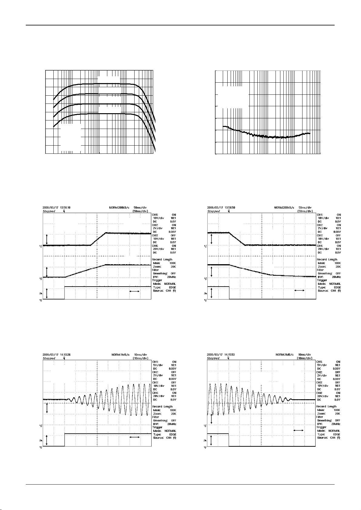
10V/div.
FILP
2V/div.
10V/div.
PDX
50ms/div.
Vcc=24V
Gain=20dB
FILP=22uF
10V/div.
2V/div.
10V/div.
Speaker
Output
FILP
PDX
50ms/div.
Fig.9 Waveform when releasing Power-down Fig.10 Waveform when activating Power-down
Vcc=24V
Po=1W
fin=200Hz
Speaker
Output
Speaker
Output
Vcc=24V
Po=1W
fin=200Hz
2V/div.
10V/div.
MUTEX
10ms/div.
2V/div.
10V/div.
MUTEX
10ms/div.
Fig.11 Waveform when releasing Soft-mute Fig.12 Waveform when activating Soft-mute
www.rohm.com
5/31
© 2011 ROHM Co., Ltd. All rights reserved.
2011.10 - Rev.C
Page 6

BD5445EFV
Technical Note
●Typical Characteristics Data (SE×2ch)Measured on ROHM’s evaluation board.
26
24
22
20
18
16
14
12
10
Output Power (W/ch)
RL=8Ω
fin=1kHz
THD+n=10%
8
6
4
2
0
8 1012141618202224262830
VCC(V)
THD+n=1%
100
90
80
70
60
50
40
EFFICIENCY (%)
30
Vcc=24V
20
RL=8Ω
fin=1kHz
10
0
0 2 4 6 8 10 12 14 16 18 20
OUTPUT POWER(W/ch)
Fig.13 Power supply voltage-Output power (RL=8Ω) Fig.14 Output power-Efficiency (RL=8Ω)
1.8
1.6
1.4
1.2
1
0.8
0.6
Consumption Current (A)
0.4
0.2
0
0 5 10 15 20 25 30 35 40
Vcc=24V
RL=8Ω
fin=1kHz
TOTA L O UTPUT PO WER (W)
26
24
22
20
18
16
14
12
10
Output Power (W/ch)
RL=6Ω
fin=1kHz
THD+n=10%
8
6
4
2
0
8 1012141618202224262830
VCC(V)
THD+n=1%
Fig.15 Total output power-Current consumption (RL=8Ω) Fig.16 Power supply voltage-Output power (RL=6Ω)
100
90
80
70
60
50
40
EFFICIENCY (%)
30
www.rohm.com
6/31
© 2011 ROHM Co., Ltd. All rights reserved.
Vcc=24V
20
RL=6Ω
fin=1kHz
10
0
0 2 4 6 8 10 12 14 16 18 20
Fig.17 Output power-Efficiency (R
OUTPUT POWER(W/ch)
=6Ω) Fig.18 Total output power-Current consumption (RL=6Ω)
L
2
1.8
1.6
1.4
1.2
1
ICC(A)
0.8
0.6
0.4
0.2
0
0 5 10 15 20 25 30 35 40
Vcc=24V
RL=6Ω
fin=1kHz
TOTA L O UTPUT PO WER (W)
2011.10 - Rev.C
Page 7

BD5445EFV
Technical Note
●Typical Characteristic Data (SE×2ch)Measured on ROHM’s evaluation board.
Dotted lines of the graphs indicate continuous output power by installing additional heat sinks.
26
24
22
20
18
16
14
12
10
Output Power (W/ch)
8
6
4
2
0
Fig.19 Power supply voltage-Output power (RL=4Ω) Fig.20 Output power-Efficiency (RL=4Ω)
RL=4Ω
fin=1kHz
THD+n=10%
THD+n=1%
8 1012141618202224262830
Vcc (V)
100
90
80
70
60
50
40
EFFICIENCY (%)
30
20
10
0
0 5 10 15 20
Vcc=24V
RL=4Ω
fin=1kHz
OUTPUT POWER(W/ch)
2
1.8
1.6
1.4
1.2
1
ICC(A)
0.8
0.6
0.4
0.2
0
0 5 10 15 20 25 30 35 40
Vcc=24V
RL=4Ω
fin=1kHz
TOTA L O UTPUT PO WER (W)
Fig.21 Total output power-Current consumption (R
=4Ω)
L
www.rohm.com
7/31
© 2011 ROHM Co., Ltd. All rights reserved.
2011.10 - Rev.C
Page 8

BD5445EFV
●Typical Characteristic Data (SE×2ch)Measured on ROHM’s evaluation board.
Dotted lines of the graphs indicate continuous output power by installing additional heat sinks.
100
10
Vcc=24V
RL=8Ω
BW=20~20kHz
100
10
Vcc=24V
RL=8Ω
Po=1W
BW=20~20kHz
1
THD+N(%)
0.1
6kHz
1
THD+N(%)
1kHz
0.1
Technical Note
0.01
0.001 0.01 0.1 1 10 100
OUTPUT POWER(W)
Fig.22 Output power-THD+n Fig.23 Frequency-THD+n
40
35
30
25
20
15
10
VOLTAGE GAIN(dB)
Vcc=24V
RL=8Ω
5
Po=1W
0
L=47uH
C=0.39uF
-5
-10
10 100 1000 10000 100000
FREQUENCY(Hz)
Fig.24 Frequency-Voltage gain Fig.25 FFT of Output Noise Voltage
100Hz
Gain=38dB
Gain=32dB
Gain=26dB
Gain=20dB
0.01
10 100 1000 10000 100000
0
-20
Vcc=24V
RL=8Ω
-40
No Signal
BW=20~20kHz
-60
-80
NOISE FFT(dBV)
-100
-120
-140
10 100 1000 10000 100000
FREQUENCY(Hz)
FREQUENCY(Hz)
50
45
40
35
30
25
20
Ou pu t P ow er (W)
15
10
5
0
8 1012141618202224262830
Fig.26 Power supply voltage-Output power (R
www.rohm.com
8/31
© 2011 ROHM Co., Ltd. All rights reserved.
Vc c (V)
=8Ω) Fig.27 Output power-Efficiency (RL=8Ω)
L
100
90
80
70
60
50
40
EFFICIENCY (%)
30
20
10
0
0 5 10 15 20 25 30 35 40
Vcc=24V
RL=8Ω
fin=1kHz
OUTPUT POWER(W/ch)
2011.10 - Rev.C
Page 9

BD5445EFV
●Typical Characteristics Data (BTL) Measured on ROHM’s evaluation board.
2
1.8
1.6
1.4
1.2
1
ICC(A)
0.8
0.6
0.4
0.2
0
0 5 10 15 20 25 30 35 40
Vcc=24V
RL=8Ω
fin=1kHz
TOTA L O UTPUT PO WER (W)
Fig.28 Total output power-Current consumption (R
=8Ω)
L
Technical Note
www.rohm.com
9/31
© 2011 ROHM Co., Ltd. All rights reserved.
2011.10 - Rev.C
Page 10

BD5445EFV
●Pin configuration and Block diagram
1
2
3
4
5
6
7
8
9
10
11
12
13
14
VCCA
Gain
Control
4step
Gain
Amp.
GNDA
FILA
FILP
Power down
Control
Mute
Control
Oscillator
Control
REG_G
PWM
Modulator
PWM
Modulator
High Temperature Protection
Output Short Protection
Under Voltage Protection
Driver
1
Driver
2
VCCP1
VCCP2
Technical Note
28
27
26
25
REG_G
24
23
22
21
20
19
REG_G
18
17
16
15
www.rohm.com
10/31
© 2011 ROHM Co., Ltd. All rights reserved.
2011.10 - Rev.C
Page 11

BD5445EFV
●Pin function explanation (Provided pin voltages are typ. values)
Pin
No.
Pin name Pin voltage Pin explanation Internal equivalence circuit
1 VCCA Vcc Power supply pin for Analog signal
2
3
GAIN0
GAIN1
-
Gain control pin
4
5
IN1
IN2
2.5V ch1 Analog signal input pin
ch2 Analog signal input pin
Input audio signal via a capacitor.
6 GNDA 0V Gnd pin for Analog signal
7 FILA 2.5V Bias pin for Analog signal
Please connect the capacitor.
8 FILP
2~4V
Bias pin for PWM signal
Please connect the capacitor.
9 ROSC 2.5V Internal PWM sampling clock frequency
setting pin
Please connect the resister setting Master
mode.
Please connect the capacitor setting Slave
mode.
10 PDX
-
Power down control pin
H: Power down OFF
L: Power down ON
4/5
1
8
6
1
6
Technical Note
16K~40K
40K~64K
www.rohm.com
11/31
© 2011 ROHM Co., Ltd. All rights reserved.
2011.10 - Rev.C
Page 12

BD5445EFV
Pin
No.
11 MU T E X - Speaker output mute control pin
12 OSC - PWM sampling clock input and output pin
13 MS - Master mode and Slave mode control pin
14 REG_G 5.5V Internal power supply pin for Gate driver
15
16
17
18
19
20
21
Technical Note
Pin name Pin voltage Pin explanation Internal equivalence circuit
H: Mute OFF
L: Mute ON
When using 2 or more ICs, connect to these
pins.
H: Slave mode
L: Master mode
Please connect the capacitor.
VCCP2 Vcc Power supply pin for ch2 PWM signal
OUT2 0V~Vcc Output pin of ch2 PWM
Please connect to Output LPF.
BSP2 5V Boot-strap pin of ch2
Please connect the capacitor.
GNDP2
0V Gnd pin for ch2 PWM signal
www.rohm.com
12/31
© 2011 ROHM Co., Ltd. All rights reserved.
2011.10 - Rev.C
Page 13

BD5445EFV
Technical Note
Pin
No.
22
23
24
Pin name Pin voltage Pin explanation Internal equivalence circuit
GNDP1
0V Gnd pin for ch1 PWM signal
BSP1 5V Boot-strap pin of ch1
Please connect the capacitor.
25
26
OUT1 0V~Vcc Output pin of ch1 PWM
Please connect to Output LPF.
27
28
VCCP1 Vcc Power supply pin for ch1 PWM signal
●Audio input circuit (pin4 and pin5)
Connect the audio input pin with a prior-stage circuit via coupling capacitors C4 and C5. Because C4, C5 and input
impedance R4, R5 of the IC circuit compose the primary HPF, the values determine an input low-band cutoff frequency. Input
cutoff frequencies are calculated by the following formulas:
1
[]
=Cf
Hz
C4•2πR4
1
[]
=Cf
Hz
C5•2πR5
An excessively high capacitance of an input coupling capacitor results in a longer period required for stabilizing a power input
pin voltage after turning on the power supply. Note that placing the MUTEX pin (pin11) at "L" level (mute turned off) for
avoidance of Pop-noise before stabilizing an input pin. R4 and R5 are changed by Gain setting.
GAIN1
(3pin)
GAIN0
(2pin)
R4,R5 input
impedance(TYP.)
Amplifier Gain (SE) Amplifier Gain (BTL)
L L 40kΩ 14dB 20dB
L H 40kΩ 20dB 26dB
H L 26.7kΩ 26dB 32dB
H H 16kΩ 32dB 38dB
C4
R4
4
Prior-stage
circuit
C5
R5
5
Fig. 29 Coupling capacitors of audio input pins
www.rohm.com
13/31
© 2011 ROHM Co., Ltd. All rights reserved.
2011.10 - Rev.C
Page 14

BD5445EFV
Technical Note
●Output LC Filter Circuit (Pins 17, 18, 25, and 26)
An output filter is required to eliminate radio-frequency components exceeding the audio-frequency region supplied to a load
(speaker). Because this IC uses sampling clock between 480kHz and 720kHz in the output PWM signals, the high-frequency
components must be appropriately removed.
This section takes an example of an LC type LPF, in which coil L
fil and capacitor Cfil compose a differential filter with an
attenuation property of -12dB/oct. A large part of switching currents flow to capacitor Cfil, and only a small part of the currents
flow to speaker R
L. The following is a table for output LC filter constants.
Speaker RL L
[μH] C
fil
[μF] C
fil1
fil2
[μF]
4Ω 22 0.68 ―
SE output
6Ω 33 0.47 ―
8Ω 47 0.39 ―
4Ω 15 0.22 1
BTL output
6Ω 22 0.15 0.68
8Ω 33 0.1 0.47
In SE(single end) applications, the dc blocking capacitor (Cse) and speaker impedance compose the primary HPF. The cutoff
frequency is determined by
=Cf
2πC
SE
1
[]
Hz
R•
L
The following table is Cse setting at cutoff frequency 20Hz, 40Hz, and 60Hz.
R
L
fc=60Hz fc=40Hz fc=20Hz
CSE[μF]
4Ω 680 1000 2200
6Ω 470 680 1500
8Ω 330 470 1000
Fig.30 SE filter configuration
Fig.31 BTL filter configuration
www.rohm.com
14/31
© 2011 ROHM Co., Ltd. All rights reserved.
2011.10 - Rev.C
Page 15

BD5445EFV
Technical Note
●Control pins function
①GAIN0, GAIN1 function
GAIN1
(Pin 3)
GAIN0
(Pin 2)
Amplifier Gain (SE) Amplifier Gain (BTL)
L L 14dB 20dB
L H 20dB 26dB
H L 26dB 32dB
H H 32dB 38dB
②MUTEX, PDX function
MUTEX
(Pin 11)
PDX
(Pin 10)
Speaker output Power down
L L HiZ_Low ON
L H Mute OFF
H H Normal operation OFF
H L Forbidden
③MS function
MS
(13pin)
Mode
L Master mode
H Slave mode
Please connect ROSC terminal (pin 9) to 22kohm resister for setting master mode.
※
※Please connect to the following filter, and input clock (duty = 50%) to OSC terminal (pin 12) for setting slave mode.
PWM Sampling frequency is sited from input clock. If input clock have noise (ex.Jitter), noise appear to Speaker output.
High level input voltage (Max.voltage) of tease control pin is equal to Vcc voltage. But absolute max.voltage of
※
In0(pin4),ROSC(pin9),OSC(pin12) and REG_G(pin14) is 5.3V. Tease pins may break, when short next pins. If these pins
short to Vcc, connecting through 10k
Fig.32 ROSC terminal filter circuit for setting slave mode.
Ω resister prevent IC from destruction.
Vcc
10kΩ
BD5445EFV
pin2
pin3
pin10
pin11
pin13
Fig.33
www.rohm.com
15/31
© 2011 ROHM Co., Ltd. All rights reserved.
2011.10 - Rev.C
Page 16

BD5445EFV
●Power supply start-up sequence
VCCA(1pin)
VCCP1(27,28pin)
VCCP2(15,16pin)
PDX(10pin)
①PDX set high after power supply voltage
is stabilized sufficiency.
MUTEX(11pin)
FILP(8pin)
OUT1(25,26pin)
OUT2(17,18pin)
Speaker output
800msec(typ.)
Technical Note
②MUTEX set high after speaker output dc voltage is stabilized sufficiency.
Sotf-start
55msec(typ.)
t
t
t
t
t
t
www.rohm.com
16/31
© 2011 ROHM Co., Ltd. All rights reserved.
2011.10 - Rev.C
Page 17

BD5445EFV
●Power supply shut-down sequence
Power supply shut down, after PDX (Pin 10) change H→L. The IC has possibly to sound POP noise, if PDX (Pim10) keep
H. Speaker’s coupling capacitor (Fig30:Cse) don’t discharge at this time. Pop-noise may sound when power supply start up
at the next time.
Technical Note
www.rohm.com
17/31
© 2011 ROHM Co., Ltd. All rights reserved.
2011.10 - Rev.C
Page 18

BD5445EFV
Technical Note
●Power supply start-up and shut-down sequence for single control
Short between PDX(Pin 10) and MUTEX(Pin 11), enable to control these pins at one time.
PDX (Pin 10) and MUTEX (Pin 11) set low at one time, while this IC is on normal mode, the IC don't operate soft-mute. If low
frequency and high level signal input this time, the IC has possibility to sound POP-Noise. To avoid this POP-Noise configure
the following circuit, because PDX (Pin10) enables to change low after MUTEX (Pin11) have changed. This sequence make
less POP-Noise because the IC can operate soft-mute.
PD/MUTE Control
MUTEX
R
10
C
10
PDX
11
10
110KΩ
90KΩ
110KΩ
90KΩ
τH=R10×C10
τL=(R10+200KΩ)×C10
Control configuration for soft-mute operation by single control
www.rohm.com
18/31
© 2011 ROHM Co., Ltd. All rights reserved.
2011.10 - Rev.C
Page 19

BD5445EFV
Technical Note
●About the protection function
Protection
function
Detecting
Output short
protection
condition
Releasing
condition
High
temperature
protection
Detecting
condition
Releasing
condition
Detecting
Under voltage
protection
condition
Releasing
condition
※ All protection functions are restored automatically when the fault is removed.
Detecting & Releasing condition
Detecting current = 10A (TYP.) HiZ_Low
Release from Vcc or Gnd short
Chip temperature to be above 150℃ (TYP.) HiZ_Low
Chip temperature to be below 125℃ (TYP.)
Power supply voltage to be below 8V (TYP.) HiZ_Low
Power supply voltage to be above 9V (TYP.)
PWM
Output
Normal
operation
Normal
operation
Normal
operation
1)Output short protection(Short to the power supply)
This IC has the output short protection circuit that stops the PWM output when the PWM output is short-circuited to the
power supply due to abnormality.
Detecting condition – It will detect when PDX pin is set High and the current that flows in the PWM output pin becomes
10A(TYP.) or more. The PWM output instantaneously enters the state of HiZ-Low if detected, and IC
does the latch.
Releasing method – This IC detect releasing from Vcc short every 220msec(TYP.). Normal operation is restored when
releasing from Vcc short.
Vcc short
Release from Vcc short
OUT1(Pin 25,26)
OUT2(Pin 17,18)
Current
10A(TYP.)
Speaker output
: Vcc short
Speaker output
: Hiz-Low release
from Vcc short
Speaker output
: Normal operation
IC restores automatically
release from Vcc short
t
www.rohm.com
19/31
© 2011 ROHM Co., Ltd. All rights reserved.
2011.10 - Rev.C
Page 20

BD5445EFV
2)Output short protection(Short to Gnd)
This IC has the output short protection circuit that stops the PWM output when the PWM output is short-circuited to Gnd due
to abnormality.
Detecting condition – It will detect when PDX pin is set High and the current that flows in the PWM output terminal becomes
10A(TYP.) or more. The PWM output instantaneously enters the state of HiZ-Low if detected, and IC
does the latch.
Releasing method – This IC detect releasing from Gnd short every 220msec(TYP.). Normal operation is restored when
releasing from Gnd short.
(※)Remark of output short protection
Circuit current changes suddenly, when IC detects output short protection. At this time IC may break, because supply
voltage rise up by back electromotive force. Decoupling capacitors (VCCPI and VCCP2) should be placed as close to the
IC as possible. (recommend 4.7μF or more.)
Technical Note
www.rohm.com
20/31
© 2011 ROHM Co., Ltd. All rights reserved.
2011.10 - Rev.C
Page 21

BD5445EFV
3)High temperature protection
This IC has the high temperature protection circuit that prevents thermal reckless driving under an abnormal state for the
temperature of the chip to exceed Tjmax=150℃.
Detecting condition - It will detect when PDX pin is set High and the temperature of the chip becomes 150℃(TYP.) or more.
The speaker output is muted through a soft-mute when detected.
Releasing condition - It will release when PDX pin is set High and the temperature of the chip becomes 120℃(TYP.) or less.
The speaker output is outputted through a soft-start when released.
Technical Note
www.rohm.com
21/31
© 2011 ROHM Co., Ltd. All rights reserved.
2011.10 - Rev.C
Page 22

BD5445EFV
Technical Note
4)Under voltage protection
This IC has the under voltage protection circuit that make speaker output mute once detecting extreme drop of the power
supply voltage.
Detecting condition – It will detect when PDX pin is set High and the power supply voltage becomes lower than 8V.
The speaker output is muted when detected.
Releasing condition – It will release when PDX pin is set High and the power supply voltage becomes more than 9V.
The speaker output is outputted through a soft-start when released.
VCCA (1pin)
VCCP1 (27,28pin)
VCCP2 (15,16pin)
8V
9V
OUT1 (25, 26pin)
OUT2 (17, 18pin)
Out put : HiZ-Low
Speaker
output
Soft-start
55msec(typ.)
800msec(typ.)
t
t
t
www.rohm.com
22/31
© 2011 ROHM Co., Ltd. All rights reserved.
2011.10 - Rev.C
Page 23

BD5445EFV
●Application Circuit Example ( single-ended output ×2 )
Technical Note
+
+
www.rohm.com
23/31
© 2011 ROHM Co., Ltd. All rights reserved.
2011.10 - Rev.C
Page 24

BD5445EFV
g
Technical Note
●BOM List ( single-ended output ×2 )
Parts Parts No. V alue Company Product No.
IC U1
Inductor L17, L25 47μH TOKO A7503AY-470M
Res is tor ROHM
R1 10 Ω MCR18EZHF10R0 1/4W F(±1%) 3.2mm×1.6mm
R9A 22 kΩ MCR01MZPF2202 1/16W F(±1%) 1.0mm×0.5mm
R17,R25 15Ω MCR18EZHF15R0 1/4W F(±1%) 3.2mm×1.6mm
C1 1 0μF GRM32DF51H106ZA01 50V
C19, C24 4.7uF GRM21BB31C475KA87 16V B(±10%
-
ROHM BD5444EFV
Capacitor MURA TA
Electrolytic
Capacitor
C15A, C27A 4.7uF GRM31CF11H475ZA01 50V
C17A, C25A 0.39uF GRM32MB11H394KA 01 50V B(±10%
C14 3. 3μF GRM188B31A335KE15 10V B(±10%
C4, C5 , C7 1 μF GRM185B30J105KE25 6.3V B(±10%
C17B, C25B 330pF GRM188B11H331KA01 50V B(±10%
C15B, C17C, C25C,
C27 B
C8 100uF 16ZLH100M 16V ±20% φ5mm×11mm
470μF 35ZLH470M 35V ±20% φ10mm×16mm
Rubycon
Rat ed
Volta
Tolerance Size
e
--
-
±20% φ11mm×13.5mm
Y5V
(+80% /
-20%)
F (+80% /
-20%)
)
)
)
)
)
9.7mm×6.4mm
3.2mm×2.5mm
2.0mm×1.2mm
3.2mm×1.6mm
3.2mm×2.5mm
1.6mm×0.8mm
1.6mm×0.8mm
1.6mm×0.8mm
※1) Please change the following parts, when using RL=6Ω speaker.
(
Inductor L17, L25 33μH TOKO A 7503AY -330M
Res is tor R1 7, R25 10Ω ROHM MCR1 8EZHF10 R0 1 /4W F(±1 %) 3 .2mm×1 .6 mm
Capacitor
C17A, C25A 0.47μF GRM32MB11H474KA 01 50V B(±10%
C17B, C25B 680pF GRM188B11H681KA01 50V B(±10%
C17C, C25C 680μF Rubycon 35ZLH680M 35V ±20% φ10mm×23mm
MURA T A
-
±20% φ11mm×13.5mm
3.2mm×2.5mm
)
1.6mm×0.8mm
)
※2) Please change the following parts, when using RL=4Ω speaker.
(
Inductor L17, L25 22μH TOKO A 7503AY-220M - ±20% φ11mm×13.5mm
Res is tor R1 7, R25 5 .6Ω ROHM MCR18EZHFL5R60 1/4W F(±1%) 3.2mm×1.6mm
Capacitor
C17A, C25A 0.68μF GRM32NB11H684KA01 50V B(±10%
C17B, C25B 1000pF GRM188B11H102KA01 50V B(±10%
C17C, C25C 1000μF Rubycon 35ZLH1000M 35V ±20% φ12.5mm×20mm
MURA T A
)
)
3.2mm×2.5mm
1.6mm×0.8mm
www.rohm.com
24/31
© 2011 ROHM Co., Ltd. All rights reserved.
2011.10 - Rev.C
Page 25

BD5445EFV
Technical Note
●Application Circuit Example ( BTL output )
VCC
10μF
Gain
Control
IN1
Differential
Input
IN2
Power down
Control
Mute
Control
CLK/IO
Master/Slave
3.3μF
C1
C14
R1
10Ω
1μF
1μF
1μF
+
100μF
R9A
22KΩ
C27BC27A
470μF4.7μF
Driver
1
Driver
2
VCCP1
VCCP2
REG_G
REG_G
28
4.7μF
4.7μF
VCC
R25
15Ω
L25
33μH
C24
C25A
0.1μF
C17A
0.1μF
C19
L17
33μH
R17
15Ω
C15BC15A
470μF4.7μF
27
C25B
330pF
26
25
24
23
22
21
20
19
18
17
C17B
330pF
16
15
VCCA
1
2
Gain
Control
3
4
10
11
12
13
14
5
6
7
8
9
4step
Gain
Amp.
GNDA
FILA
FILP
Power down
Control
Mute
Control
Oscillator
Control
REG_G
High Temperature Protection
C4
C5
C7
C8
PWM
Modulator
PWM
Modulator
Output Short Protection
Under Voltage Protection
C17D
0.47μF
8Ω
www.rohm.com
25/31
© 2011 ROHM Co., Ltd. All rights reserved.
2011.10 - Rev.C
Page 26

BD5445EFV
g
Technical Note
●BOM List ( BTL output )
Parts Parts No. Value Company Product No.
IC U1
Inductor L17, L25 33μH TOKO A 7503AY-330M
Res is tor ROHM
R1 10Ω MCR18EZHF10R0 1/4W F(±1%) 3.2mm×1.6mm
R9A 22 kΩ MCR01MZPF2202 1/16W F(±1%) 1.0mm×0.5mm
R17,R25 15Ω MCR18EZHF15R0 1/4W F(±1%) 3.2mm×1.6mm
C1 10 μF GRM32DF51H106ZA01 50V
-
ROHM BD5444EFV
Capacitor MURATA
Electrolytic
Capacitor
C19, C24 4.7uF GRM21BB31C475KA87 16V B(±10%
C15A, C27A 4.7uF GRM31CF11H475ZA01 50V
C17A, C25A 0.1uF GRM188B31H104KA92 50V B(±10%
C17D 0.47uF GRM32MB11H474LA01 50V B(±20%
C14 3. 3μF GRM188B31A335KE15 10V B(±10%
C4, C5 , C7 1 μF GRM185B30J105KE25 6.3V B(±10%
C17B, C25B 330pF GRM188B11H331KA01 50V B(±10%
C15B, C27B 470μF 35ZLH470M 35V ±20% φ10mm×16mm
C8 100uF 16ZLH100M 16V ±20% φ5mm×11mm
Rubycon
Rat ed
Volta
Toleranc e Size
e
--
-
±20% φ11mm×13.5mm
Y5V
(+80% /
-20%)
)
F (+80% /
-20%)
)
)
)
)
)
9.7mm×6.4mm
3.2mm×2.5mm
2.0mm×1.2mm
3.2mm×1.6mm
1.6mm×0.8mm
3.2mm×2.5mm
1.6mm×0.8mm
1.6mm×0.8mm
1.6mm×0.8mm
※1) Please change the following parts, when using RL=6Ω speaker.
(
Inductor L17, L25 22μH TOKO A 7503AY-220M
Res is tor R1 7, R25 1 0Ω ROHM MCR1 8EZHF 10R0 1 /4W F( ±1 %) 3. 2mm×1 .6 mm
Capacitor MURATA
C17A, C25A 0.15μF GRM21BB31H154MA88 50V B(±20%
C17B, C25B 680pF GRM188B11H681KA01 50V B(±10%
C17D 0.68μF GRM32NB11H684MA01 50V B(±20%
-
±20% φ11mm×13.5mm
2.0mm×1.2mm
)
1.6mm×0.8mm
)
3.2mm×2.5mm
)
※2) Please change the following parts, when using RL=4Ω speaker.
(
Inductor L17, L25 15μH TOKO A 7503AY -150M
Res is tor R1 7, R25 5.6 Ω ROHM MCR18EZHFL5R60 1/4W F(±1%) 3.2mm×1.6mm
Capacitor MURATA
C17A, C25A 0.22μF GRM21BB31H224MA88 50V B(±20%
C17B, C25B 1000pF GRM188B11H102KA01 50V B(±10%
C17D 1μF GRM31MB31H105KA 87 50V B(±20%
-
±20% φ11mm×13.5mm
2.0mm×1.2mm
)
1.6mm×0.8mm
)
3.2mm×2.5mm
)
www.rohm.com
26/31
© 2011 ROHM Co., Ltd. All rights reserved.
2011.10 - Rev.C
Page 27

BD5445EFV
●Application Circuit Example ( 2.1ch output )
VCC
Technical Note
10μF
Control
IN1
IN2
Power down
Control
Mute
Control
Master (L input)
3.3μF
C1
Gain
Clock output
C14
R1
10Ω
1μF
+
100μF
R9A
22KΩ
C4
1μF
C5
1μF
C7
C8
10
12
13
14
11
1
2
3
4
5
6
7
8
9
VCCA
Gain
Control
4step
Gain
Amp.
GNDA
FILA
FILP
Power down
Control
Mute
Control
Oscillator
Control
REG_G
Master
PWM
Modulator
PWM
Modulator
High Temperature Protection
Output Short Protection
Under Voltage Protection
Driver
1
Driver
2
VCCP1
VCCP2
REG_G
REG_G
C27BC27A
470μF4.7μF
28
C25B
330pF
C17B
330pF
R25
15Ω
L25 C25C
47μH
C24
4.7μF
C25A
0.39μF
C17A
0.39μF
C19
4.7μF
L17
47μH
R17
15Ω
VCC
C15BC15A
470μF4.7μF
470μF
+
+
C17C
470μF
8Ω
8Ω
27
26
25
24
23
22
21
20
19
18
17
16
15
VCC
C1
10μF
Gain
C14
R1
10Ω
100μF
C9A
2200pF
Clock input
C4
1μF
C5
1μF
C7
1μF
+
C8
10
12
13
14
11
1
2
3
4
5
6
7
8
9
VCCA
Gain
Control
4step
Gain
Amp.
GNDA
FILA
FILP
Power down
Control
Mute
Control
Oscillator
Control
REG_G
Slave
PWM
Modulator
PWM
Modulator
High Temperature Protection
Output Short Protection
Under Voltage Protection
Driver
1
Driver
2
VCCP1
VCCP2
REG_G
REG_G
C27BC27A
470μF4.7μF
28
C25B
330pF
C17B
330pF
4.7μF
4.7μF
VCC
R25
15Ω
L25
33μH
C24
C25A
0.1μF
C17A
0.1μF
C19
L17
33μH
R17
15Ω
C17D
0.47μF
8Ω
C15BC15A
470μF4.7μF
27
26
25
24
23
22
21
20
19
18
17
16
15
Differential
Input
Control
IN1
IN2
R9B
22KΩ
C9B
220pF
Power down
Control
Mute
Control
Slave (H input)
3.3μF
www.rohm.com
27/31
© 2011 ROHM Co., Ltd. All rights reserved.
2011.10 - Rev.C
Page 28

BD5445EFV
g
●BOM List ( 2.1ch output )
Technical Note
Parts Parts No. Value Company Product No.
Resistor R9B 22kΩ ROHM MCR01MZPF2202 1/16W F(±1%) 1.0mm×0.5mm
Capacitor MURATA
(
※) Parts are written used at "Slave mode" only. Please use same parts written P23 ~ P26.
C9A 2200pF GRM155R61A222KA01 10V X5R(±10%)1.0mm×0.5mm
C9B 220pF GRM1552C1E221JA01 25V CH(±5%)1.0mm×0.5mm
Rated
Volta
Tolerance Size
e
www.rohm.com
28/31
© 2011 ROHM Co., Ltd. All rights reserved.
2011.10 - Rev.C
Page 29

BD5445EFV
●Notes for use
1 ) Absolute maximum ratings
Use of the IC in excess of absolute maximum ratings such as the applied voltage or operating temperature range may
result in IC damage. Assumptions should not be made regarding the state of the IC (short mode or open mode) when
such damage is suffered. A physical safety measure such as a fuse should be implemented when use of the IC in a
special mode where the absolute maximum ratings may be exceeded is anticipated.
2 ) Power supply lines
As return of current regenerated by back EMF of output coil happens, take steps such as putting capacitor between
power supply and Gnd as a electric pathway for the regenerated current. Be sure that there is no problem with each
property such as emptied capacity at lower temperature regarding electrolytic capacitor to decide capacity value. If the
connected power supply does not have sufficient current absorption capacity, regenerative current will cause the
voltage on the power supply line to rise, which combined with the product and its peripheral circuitry may exceed the
absolute maximum ratings. It is recommended to implement a physical safety measure such as the insertion of a
voltage clamp diode between the power supply and Gnd pins.
3 ) Gnd potential (Pin 6, 20, 21, 22, 23)
Ensure a minimum Gnd pin potential in all operating conditions.
4 ) Input terminal
The parasitic elements are formed in the LSI because of the voltage relation. The parasitic element operating causes
the wrong operation and destruction. Therefore, please be careful so as not to operate the parasitic elements by
impressing to input terminals lower voltage than Gnd. Please do not apply the voltage to the input terminal when the
power-supply voltage is not impressed.
5 ) Setting of heat
Use a thermal design that allows for a sufficient margin in light of the power dissipation (Pd) in actual operating
conditions. This IC exposes its frame of the backside of package. Note that this part is assumed to use after providing
heat dissipation treatment to improve heat dissipation efficiency. Try to occupy as wide as possible with heat dissipation
pattern not only on the board surface but also the backside.
Class D power amplifier is High efficiency and low heat generation by comparison with conventional Analog power
amplifier. However, In case it is operated continuously by maximum output power, Power dissipation(Pdiss) may
exceed package dissipation. Please consider about heat design that Power dissipation(Pdiss) does not exceed
Package dissipation(Pd) in average power(Poav). (Tjmax :Maximum junction temperature=150℃, Ta :Peripheral
temperature[℃], θja :Thermal resistance of package[℃/W], Poav:Average power[W], η:Efficiency)
Package dissipation: Pd (W) = (Tjmax - Ta)/θja
Power dissipation: Pdiss(W) = Poav * (1
Actions in strong magnetic field
6 )
Use caution when using the IC in the presence of a strong magnetic field as doing so may cause the IC to malfunction.
7 ) Thermal shutdown circuit
This product is provided with a built-in thermal shutdown circuit. When the thermal shutdown circuit operates, the
output transistors are placed under open status. The thermal shutdown circuit is primarily intended to shut down the IC
avoiding thermal runaway under abnormal conditions with a chip temperature exceeding Tjmax = 150℃.
8 ) Shorts between pins and misinstallation
When mounting the LSI on a board, pay adequate attention to orientation and placement discrepancies of the LSI. If it
is misinstalled and the power is turned on, the LSI may be damaged. It also may be damaged if it is shorted by a
foreign substance coming between pins of the LSI or between a pin and a power supply or a pin and a Gnd
9 ) Power supply on/off (Pin 1, 15, 16, 27, 28)
In case power supply is started up, PDX (Pin 10) and MUTEX (Pin 11) always should be set LOW, And in case power
supply is shut down, it should be set LOW likewise. Then it is possible to eliminate pop noise when power supply is
turned on/off. And also, all power supply terminals should start up and shut down together.
10 ) Precautions for Speaker-setting
If the impedance characteristics of the speakers at high-frequency range while increase rapidly, the IC might not have
stable-operation in the resonance frequency range of the LC-filter. Therefore, consider adding damping-circuit, etc.,
depending on the impedance of the speaker.
/η- 1)
Technical Note
www.rohm.com
29/31
© 2011 ROHM Co., Ltd. All rights reserved.
2011.10 - Rev.C
Page 30

BD5445EFV
●Allowable Power Dissipation
Measuring instrument:TH-156(Kuwano Electrical Instruments Co., Ltd.)
Measuring conditions:Installation on ROHM’s board
Board size:70mm×70mm×1.6mm(with thermal via on board)
Material:FR4
・The board on exposed heat sink on the back of package are connected by soldering.
PCB①:1-layer board(back copper foil size: 0mm×0mm), θja=86.2℃/W
PCB②:2-layer board(back copper foil size: 70mm×70mm),θja=37.8℃/W
PCB③:4-layer board(back copper foil size: 70mm×70mm),θja=26.6℃/W
6
PCB③ 4.7W
PCB③ 4.7W
5
4
PCB② 3.3W
PCB② 3.3W
3
2
PCB① 1.45W
PCB① 1.45W
Power dissipatio n :Pd (W)
1
0
0 102030405060708090100110120130140150
Ambient temperature :Ta (℃)
Technical Note
www.rohm.com
30/31
© 2011 ROHM Co., Ltd. All rights reserved.
2011.10 - Rev.C
Page 31

BD5445EFV
●Ordering part number
B D 5 4 4 5 E F V - E 2
Part No. Part No.
HTSSOP-B28
9.7±0.1
(MAX 10.05 include BURR)
(5.5)
1528
4.4±0.1
6.4±0.2
1.0MAX
0.625
141
1PIN MARK
0.85±0.05
0.08±0.05
0.65
0.24
+0.05
-
0.04
(2.9)
0.08 S
0.08
S
M
+
6
°
4
°
−4°
+0.05
0.17
-
(Unit : mm)
0.5±0.15
0.03
<Tape and Reel information>
1.0±0.2
Package
EFV:HTSSOP-B28
Embossed carrier tape (with dry pack)Tape
Quantity
Direction
of feed
2500pcs
E2
()
Packaging and forming specification
E2: Embossed tape and reel
The direction is the 1pin of product is at the upper left when you hold
reel on the left hand and you pull out the tape on the right hand
Reel
1pin
Order quantity needs to be multiple of the minimum quantity.
∗
Technical Note
Direction of feed
www.rohm.com
31/31
© 2011 ROHM Co., Ltd. All rights reserved.
2011.10 - Rev.C
Page 32

Notes
No copying or reproduction of this document, in part or in whole, is permitted without the
consent of ROHM Co.,Ltd.
The content specied herein is subject to change for improvement without notice.
The content specied herein is for the purpose of introducing ROHM's products (hereinafter
"Products"). If you wish to use any such Product, please be sure to refer to the specications,
which can be obtained from ROHM upon request.
Examples of application circuits, circuit constants and any other information contained herein
illustrate the standard usage and operations of the Products. The peripheral conditions must
be taken into account when designing circuits for mass production.
Great care was taken in ensuring the accuracy of the information specied in this document.
However, should you incur any damage arising from any inaccuracy or misprint of such
information, ROHM shall bear no responsibility for such damage.
The technical information specied herein is intended only to show the typical functions of and
examples of application circuits for the Products. ROHM does not grant you, explicitly or
implicitly, any license to use or exercise intellectual property or other rights held by ROHM and
other parties. ROHM shall bear no responsibility whatsoever for any dispute arising from the
use of such technical information.
The Products specied in this document are intended to be used with general-use electronic
equipment or devices (such as audio visual equipment, ofce-automation equipment, communication devices, electronic appliances and amusement devices).
The Products specied in this document are not designed to be radiation tolerant.
While ROHM always makes efforts to enhance the quality and reliability of its Products, a
Product may fail or malfunction for a variety of reasons.
Please be sure to implement in your equipment using the Products safety measures to guard
against the possibility of physical injury, re or any other damage caused in the event of the
failure of any Product, such as derating, redundancy, re control and fail-safe designs. ROHM
shall bear no responsibility whatsoever for your use of any Product outside of the prescribed
scope or not in accordance with the instruction manual.
The Products are not designed or manufactured to be used with any equipment, device or
system which requires an extremely high level of reliability the failure or malfunction of which
may result in a direct threat to human life or create a risk of human injury (such as a medical
instrument, transportation equipment, aerospace machinery, nuclear-reactor controller, fuelcontroller or other safety device). ROHM shall bear no responsibility in any way for use of any
of the Products for the above special purposes. If a Product is intended to be used for any
such special purpose, please contact a ROHM sales representative before purchasing.
If you intend to export or ship overseas any Product or technology specied herein that may
be controlled under the Foreign Exchange and the Foreign Trade Law, you will be required to
obtain a license or permit under the Law.
Notice
www.rohm.com
© 2011 ROHM Co., Ltd. All rights reserved.
Thank you for your accessing to ROHM product informations.
More detail product informations and catalogs are available, please contact us.
ROHM Customer Support System
http://www.rohm.com/contact/
R1120
A
 Loading...