ROHM BD5444EFV Technical data

Middle Power Class-D Speaker Amplifiers
Analog Input /
Single End Output
Class-D Speaker Amplifier
BD5444EFV
No.11075ECT15
●Overview
BD5444EFV is a Analog input type Class D Speaker Amplifier designed for Flat-panel TVs in particular for space-saving
and low-power consumption, delivers an output power of 20W+20W. This IC employs state-of-the-art Bipolar, CMOS, and
DMOS (BCD) process technology that eliminates turn-on resistance in the output power stage and internal loss due to line
resistances up to an ultimate level. With this technology, the IC can achieve high efficiency of 93% (10W+10W output with
8Ω load).In addition, the IC is packaged in a compact reverse heat radiation type power package to achieve low power
consumption and low heat generation and eliminates necessity of external heat-sink up to a total output power of 40W. This
product satisfies both needs for drastic downsizing, low-profile structures and powerful, high-quality playback of sound
system.
●Features
1) 20W stereo single-ended outputs
40W mono bridge-tied-load output
2) Wide supply voltage (From 10V to 27V)
3) Four selectable gain (14, 20, 26, 32dB)
4) Master / Slave function
5) Soft-start and Soft-mute
6) Low noise, Low distortion
7) Various protection functions
(High temperature, Output short, Under voltage)
8) Small power package (HTSSOP-B28)
●Applications
Flat Panel TVs (LCD, Plasma), Home Audio, Desktop PC, Amusement equipments, Electronic Music equipments, etc.
www.rohm.com
1/31
© 2011 ROHM Co., Ltd. All rights reserved.
2011.10 - Rev.C
BD5444EFV
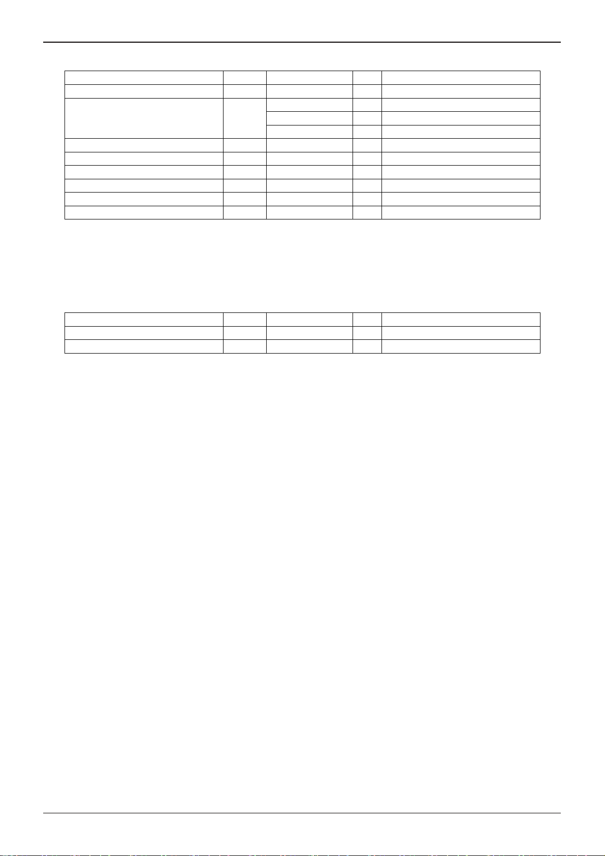
●Absolute maximum ratings (Ta=25℃)
Item Symbol Limit Unit Conditions
Supply voltage Vcc 30 V Pin 1, 15, 16, 27, 28 ※1 ※2
1.45 W ※3
Power dissipation Pd
3.30 W ※4
4.70 W ※5
Input voltage for signal VIN -0.3 ~ 5.3 V Pin 4, 5 ※1
Input voltage for control V
Input voltage for clock V
-0.3 ~ Vcc + 0.3 V Pin 2, 3, 10, 11, 13 ※1
CONT
-0.3 ~ 5.3 V Pin 12 ※1
OSC
Operating temperature range Topr -25 ~ +85 ℃
Storage temperature range Tstg -55 ~ +150 ℃
Maximum junction temperature Tjmax +150 ℃
※1 The voltage that can be applied, based on Gnd(Pin6, 20, 21, 22, 23)
※2 Do not, however exceed Pd and Tjmax=150℃.
※3 70mm×70mm×1.6mm, FR4, 1-layer glass epoxy board (Copper on bottom layer 0%)
Derating in done at 11.6mW/℃ for operating above Ta=25℃.
※4 70mm×70mm×1.6mm, FR4, 2-layer glass epoxy board (Copper on bottom layer 100%)
Derating in done at 26.4mW/℃ for operating above Ta=25℃. There are thermal via on the board.
※5 70mm×70mm×1.6mm, FR4, 4-layer glass epoxy board (Copper on bottom layer 100%)
Derating in done at 37.6mW/℃ for operating above Ta=25℃. There are thermal via on the board.
●Operating conditions (Ta=25℃)
Item Symbol Limit Unit Conditions
Supply voltage Vcc 10 ~ 27 V Pin 1, 15, 16, 27, 28 ※1 ※2
Minimum load impedance RL 3.6 Ω ※6
※6 Do not, however exceed Pd.
※ No radiation-proof design
Technical Note
www.rohm.com
2/31
© 2011 ROHM Co., Ltd. All rights reserved.
2011.10 - Rev.C
BD5444EFV
Technical Note
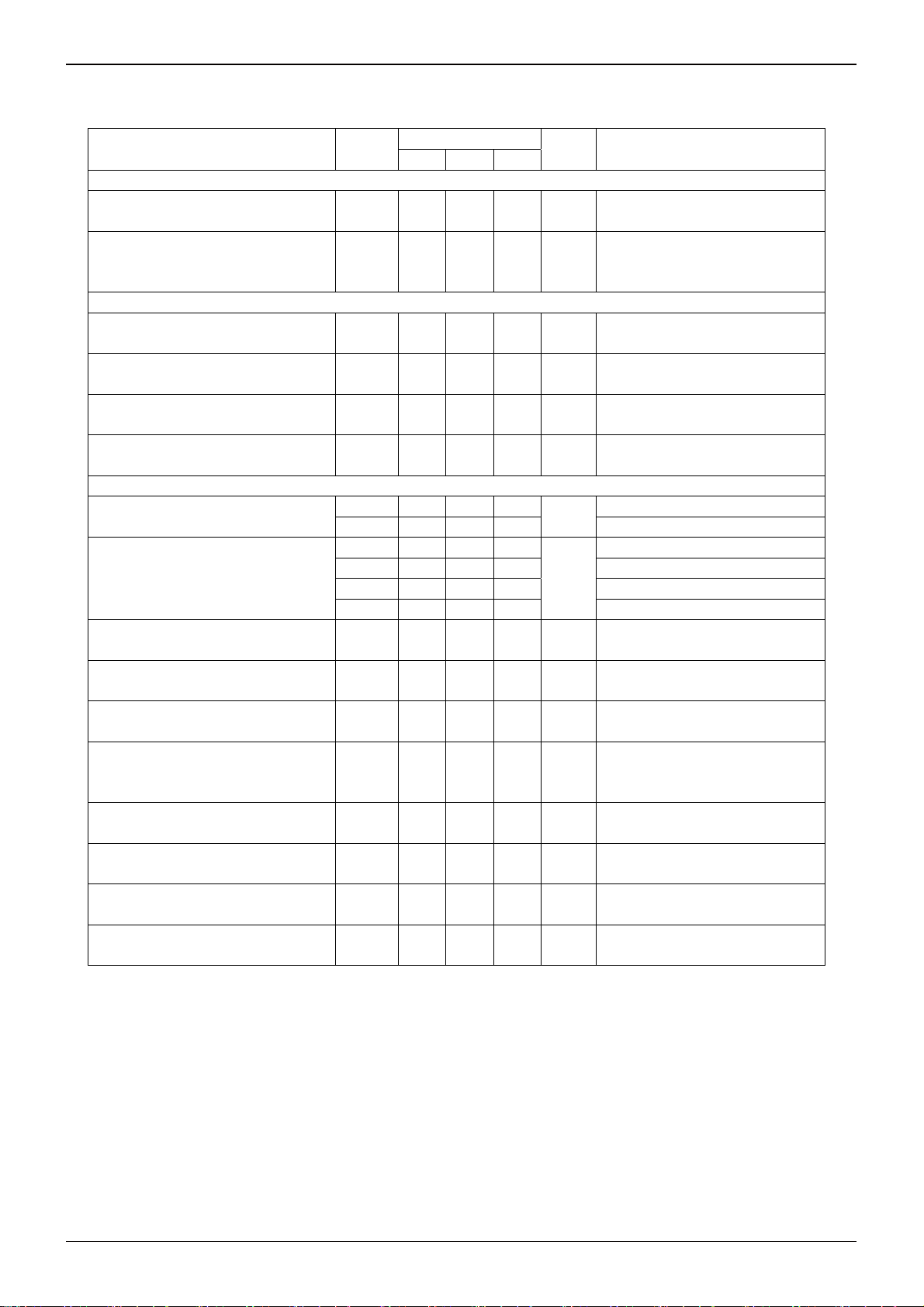
●Electrical characteristics ( Unless otherwise specified Ta=25℃, Vcc=24V, f=1kHz, RL=8Ω, Po=1W, Gain=20dB,
PDX=24V, MUTEX=24V, MS=0V, Single-ended outputs)
Item Symbol
Limit
Min Typ Max
Unit Conditions
Whole circuit
Circuit current 1 I
Circuit current 2
(Power down mode)
- 25 50 mA
CC1
I
- 2 4 mA
CC2
Pin 1, 15, 16, 27, 28
No load, No signal
Pin 1, 15, 16, 27, 28
PDX=0V,MUTEX=0V, No load, No
signal
Control circuit
High level input voltage for control VIH 2.5 - 24 V
Low level input voltage for control VIL 0 - 0.8 V
High level input voltage for clock V
Low level input voltage for clock V
2.5 - 5 V
IHC
0 - 0.8 V
ILC
Pin 2, 3, 10, 11, 13
Pin 2, 3, 10, 11, 13
Pin 12
Pin 12
Audio circuit
Momentary maximum output power
Voltage gain
PO1 - 11 -
PO2 - 20 - RL=4Ω, THD+n=10% ※7
G
12 14 16
V0
GV1 18 20 22 Gain1=0V, Gain0=24V ※7
GV2 24 26 28 Gain1=24V, Gain0=0V ※7
RL=8Ω, THD+n=10% ※7
W
Gain1=0V, Gain0=0V ※7
dB
GV3 30 32 34 Gain1=24V, Gain0=24V ※7
Total harmonic distortion THD - 0.05 - %
Crosstalk CT 60 75 - dB
Output noise voltage VNO - 80 160 μVrms
Residual noise voltage
(Power down mode)
- 1 10 μVrms
V
NOR
Mute attenuation GVM 80 94 - dB
Power supply rejection ratio PSRR - 60 - dB
Internal oscillation frequency F
External clock frequency F
※7 These items show the typical performance of device and depend on board layout, parts, power supply.
The standard value is in mounting device and parts on surface of ROHM’s board directly.
480 600 720 kHz
OSC
480 - 720 kHz
EXT
BW=20~20kHz
※7
Rg=0Ω, BW=IHF-A
※7
Rg=0Ω, BW=IHF-A
※7
PDX=0V, MUTEX=0V
Rg=0Ω, BW=IHF-A
※7
MUTEX=0V, BW= IHF-A
※7
Vripple=1Vrms, BW= IHF-A
Rg=0Ω, fripple=100Hz ※7
Pin 12, MS=0V
※7
Pin 12, MS=24V
※7
www.rohm.com
3/31
© 2011 ROHM Co., Ltd. All rights reserved.
2011.10 - Rev.C
BD5444EFV
Technical Note
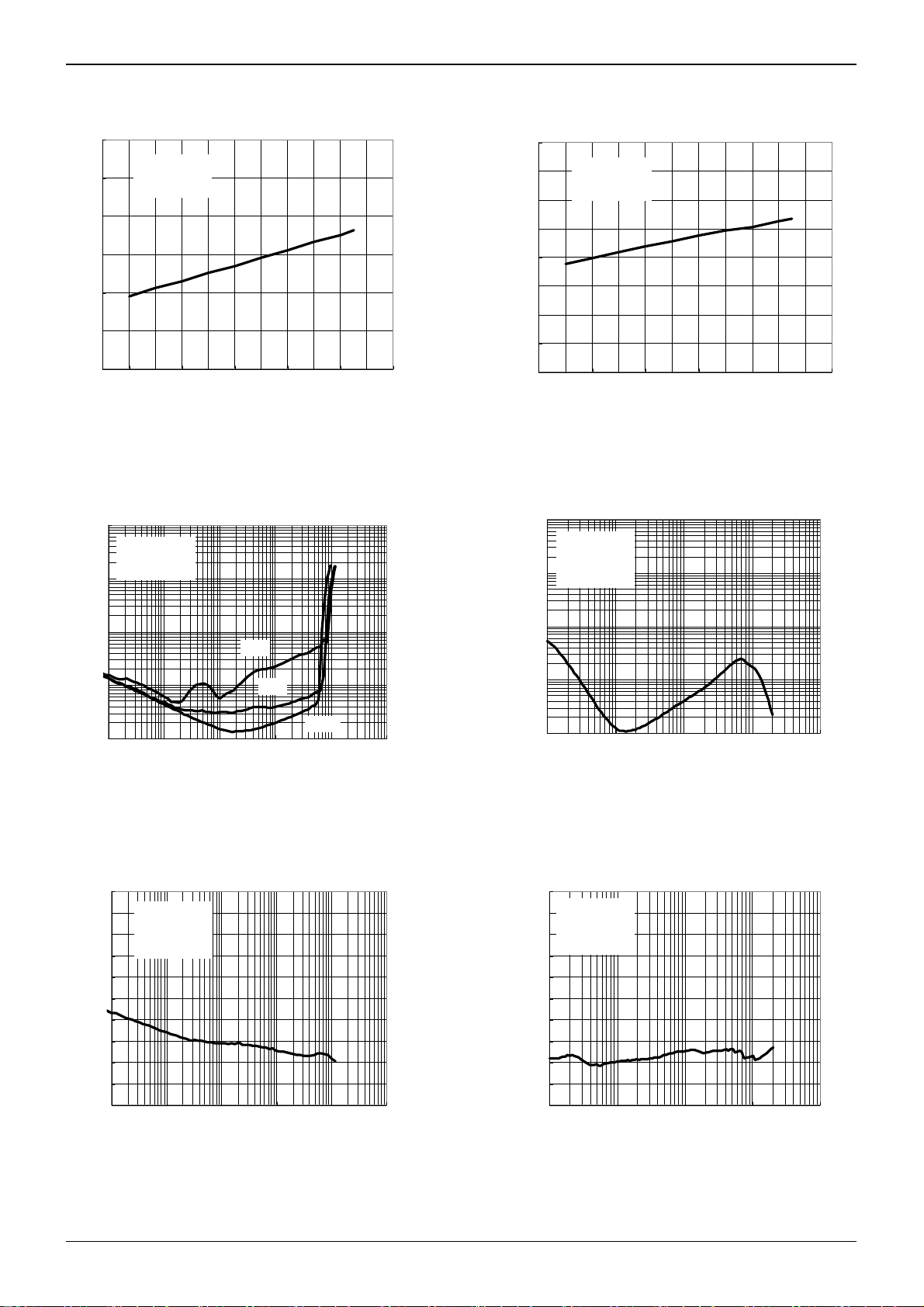
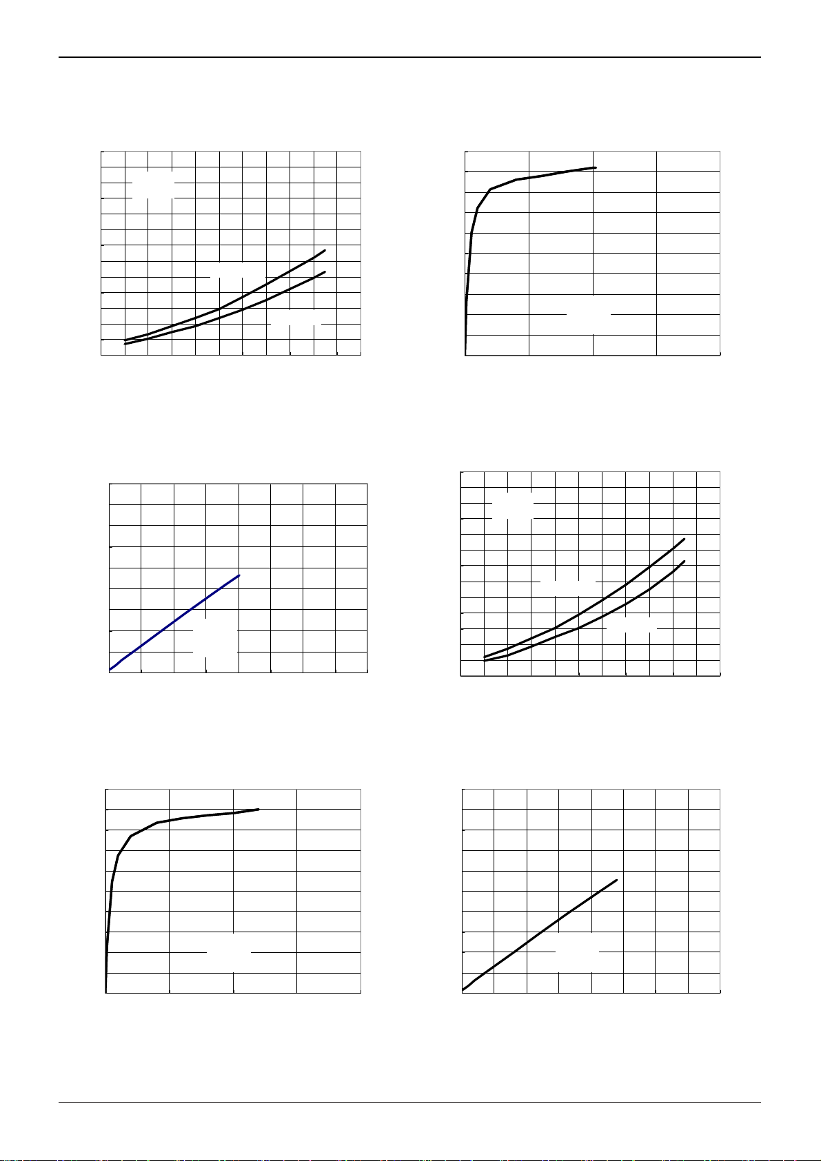
●Typical Characteristics Data (SE×2ch)Measured on ROHM’s evaluation board.
3
2.5
2
RL=8Ω
No Signal
PDX=MUTEX=L
1.5
Ic c (mA)
1
0.5
0
8 10121416 18202224 262830
Vc c (V)
40
35
30
25
20
Ic c (mA)
15
10
5
0
RL=8Ω
No Signal
PDX=MUTEX=H
8 1012141618202224262830
Vc c (V)
Fig. 1 Power supply voltage-Current consumption Fig. 2 Power supply voltage-Current consumption
100
10
Vcc=24V
RL=8Ω
BW=20~20kHz
100
10
Vcc=24V
RL=8Ω
Po=1W
BW=20~20kHz
1
THD+N(%)
6kHz
0.1
0.01
0.001 0.01 0.1 1 10 100
OUTPUT POWER(W)
1kHz
100Hz
1
THD+N(%)
0.1
0.01
10 100 1000 10000 100000
FREQUENCY(Hz)
Fig.3 Output power-THD+N Fig.4 Frequency-THD+N
0
-10
-20
-30
-40
-50
-60
CROS ST ALK (dB)
-70
-80
-90
-100
Vcc=24V
RL=8Ω
fin=1kHz
BW=20~20kHz
0.001 0.01 0.1 1 10 100
OUTPUT POWER(W)
0
Vcc=24V
-10
RL=8Ω
Po=1W
-20
BW=20~20kHz
-30
-40
-50
-60
CROS ST ALK (dB)
-70
-80
-90
-100
10 100 1000 10000 100000
FREQUENCY(Hz)
Fig.5 Output power-Crosstalk Fig.6 Frequency-Crosstalk
www.rohm.com
4/31
© 2011 ROHM Co., Ltd. All rights reserved.
2011.10 - Rev.C
BD5444EFV
Technical Note
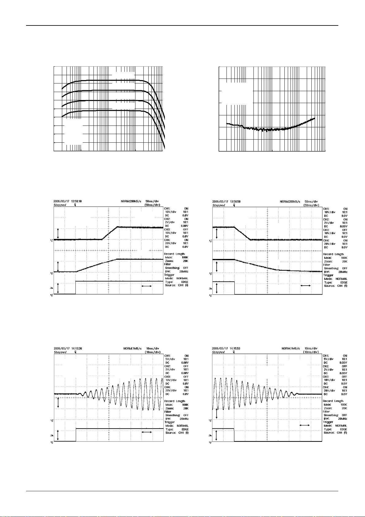
●Typical Characteristics Data (SE×2ch)Measured on ROHM’s evaluation board.
40
35
30
25
20
15
10
VOLTAGE GAIN(dB)
-5
-10
Vcc=24V
5
RL=8Ω
Po=1W
0
L=47uH
C=0.39uF
10 100 1000 10000 100000
Gain=32dB
Gain=26dB
Gain=20dB
Gain=14dB
FREQUENCY(Hz)
0
-20
Vcc=24V
RL=8Ω
-40
No Sign al
BW=20~20kHz
-60
-80
NOISE FFT(dBV)
-100
-120
-140
10 100 1000 10000 100000
FREQUENCY(Hz)
Fig.7 Frequency-Voltage gain Fig.8 FFT of Output Noise Voltage
Vcc=24V
Gain=20dB
FILP=22uF
10V/div.
Speaker
Output
2V/div.
FILP
PDX
10V/div.
50ms/div.
Vcc=24V
Gain=20dB
FILP=22uF
10V/div.
2V/div.
10V/div.
Speaker
Output
FILP
PDX
50ms/div.
Fig.9 Waveform when releasing Power-down Fig.10 Waveform when activating Power-down
Vcc=24V
Po=1W
fin=200Hz
Speaker
Output
Speaker
Output
Vcc=24V
Po=1W
fin=200Hz
2V/div.
10V/div.
MUTEX
10ms/div.
2V/div.
10V/div.
MUTEX
10ms/div.
Fig.11 Waveform when releasing Soft-mute Fig.12 Waveform when activating Soft-mute
www.rohm.com
5/31
© 2011 ROHM Co., Ltd. All rights reserved.
2011.10 - Rev.C
BD5444EFV
●Typical Characteristics Data (SE×2ch)Measured on ROHM’s evaluation board.
26
24
22
20
18
16
14
12
10
Output Power (W/ch)
8
6
4
2
0
RL=8Ω
fin=1kHz
THD+n=10%
THD+n=1%
8 1012141618202224262830
Vcc (V)
100
90
80
70
60
50
40
EFFICIENCY (%)
30
20
10
0
0 5 10 15 20
Technical Note
Vcc=24V
RL=8Ω
fin=1kHz
OUTPUT POWER(W/ch)
Fig.13 Power supply voltage-Output power (R
L
1.8
1.6
1.4
1.2
1
0.8
0.6
Consumption Current (A)
0.4
0.2
0
0 5 10 15 20 25 30 35 40
Vcc=24V
RL=8Ω
fin=1kHz
TOTA L O UTPUT PO WER (W)
Fig.15 Total output power-Current consumption (R
100
90
80
70
60
50
40
EFFICIENCY (%)
30
20
10
0
0 5 10 15 20
Vcc=24V
RL=6Ω
fin=1kHz
OUTPUT POWER(W/ch)
=8Ω) Fig.14 Output power-Efficiency (RL=8Ω)
26
24
22
20
18
16
14
12
10
Output Power (W/ch)
8
6
4
2
0
=8Ω) Fig.16 Power supply voltage-Output power (RL=6Ω)
L
2
1.8
1.6
1.4
1.2
1
ICC(A)
0.8
0.6
0.4
0.2
0
RL=6Ω
fin=1kHz
THD+n=10%
THD+n=1%
8 1012141618202224262830
Vcc (V)
Vcc=24V
RL=6Ω
fin=1kHz
0 5 10 15 20 25 30 35 40
TOTA L O UTPUT PO WER (W)
Fig.17 Output power-Efficiency (R
www.rohm.com
6/31
© 2011 ROHM Co., Ltd. All rights reserved.
=6Ω) Fig.18 Total output power-Current consumption (RL=6Ω)
L
2011.10 - Rev.C
BD5444EFV
Technical Note
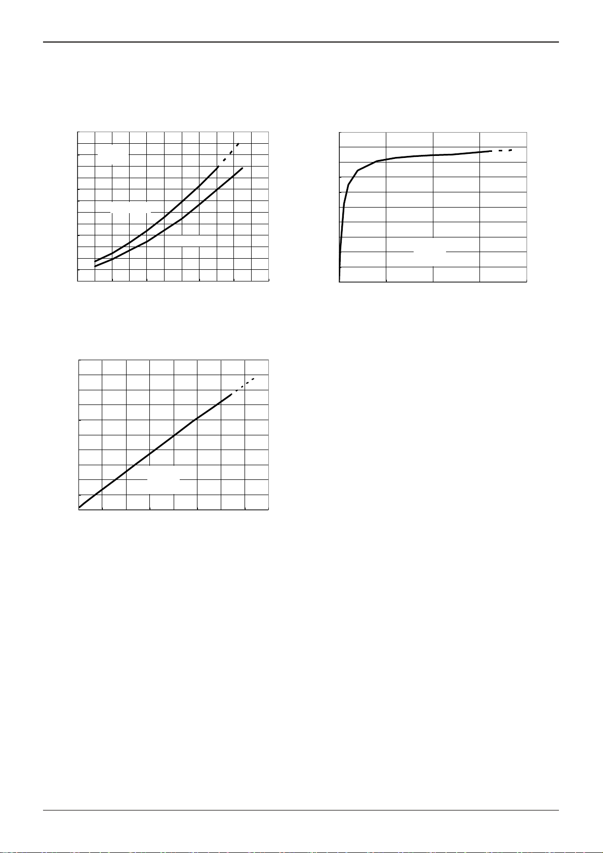
●Typical Characteristic Data (SE×2ch)Measured on ROHM’s evaluation board.
Dotted lines of the graphs indicate continuous output power by installing additional heat sinks.
26
24
22
20
18
16
14
12
10
Output Power (W/ch)
8
6
4
2
0
Fig.19 Power supply voltage-Output power (RL=4Ω) Fig.20 Output power-Efficiency (RL=4Ω)
RL=4Ω
fin=1kHz
THD+n=10%
THD+n=1%
8 1012141618202224262830
Vcc (V)
100
90
80
70
60
50
40
EFFICIENCY (%)
30
20
10
0
0 5 10 15 20
Vcc=24V
RL=4Ω
fin=1kHz
OUTPUT POWER(W/ch)
2
1.8
1.6
1.4
1.2
1
ICC(A)
0.8
0.6
0.4
0.2
0
0 5 10 15 20 25 30 35 40
Vcc=24V
RL=4Ω
fin=1kHz
TOTA L O UTPUT PO WER (W)
Fig.21 Total output power-Current consumption (R
=4Ω)
L
www.rohm.com
7/31
© 2011 ROHM Co., Ltd. All rights reserved.
2011.10 - Rev.C
BD5444EFV
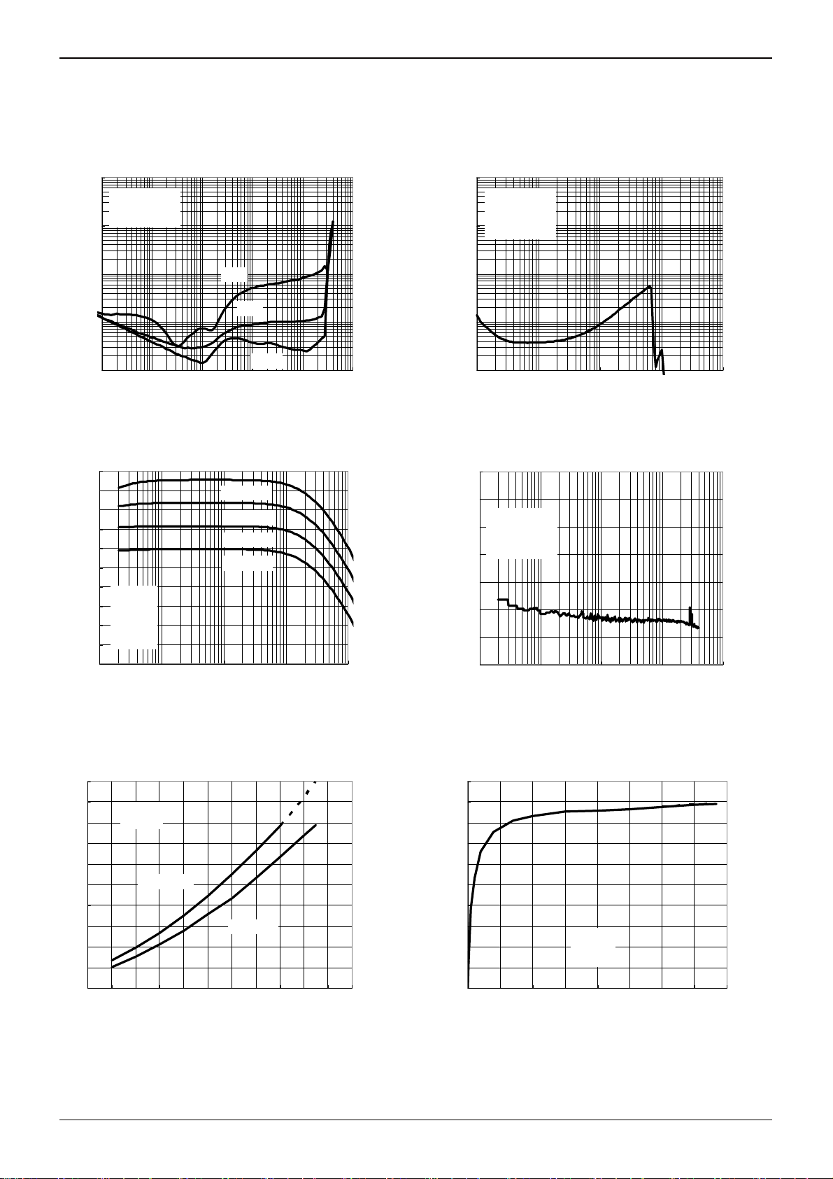
●Typical Characteristics Data (BTL) Measured on ROHM’s evaluation board.
Dotted lines of the graphs indicate continuous output power by installing additional heat sinks.
2
100
Vcc=24V
1.8
RL=8Ω
1.6
BW=20~20kHz
10
1.4
1.2
1
1
ICC(A)
THD+N(%)
0.8
0.6
0.1
0.4
0.2
0.01
0
0.001 0.01 0.1 1 10 100
0 5 10 15 20 25 30 35 40
6kHz
1kHz
Vcc=24V
RL=8Ω
fin=1kHz
OUTPUT POWER(W)
TOTA L O UTPUT PO WER (W)
100Hz
100
Vcc=24V
RL=8Ω
Po=1W
10
BW=20~20kHz
1
THD+N(%)
0.1
0.01
10 100 1000 10000 100000
FREQUENCY(Hz)
Fig.22 Output power-THD+n Fig.23 Frequency-THD+n
Technical Note
40
35
30
25
20
15
10
Vcc=24V
VOLTAGE GAIN(dB)
RL=8Ω
5
Po=1W
0
L=47uH
C=0.39uF
-5
-10
10 100 1000 10000 100000
Gain=38dB
Gain=32dB
Gain=26dB
Gain=20dB
FREQUENCY(Hz)
0
-20
Vcc=24V
RL=8Ω
-40
No Signal
BW=20~20kHz
-60
-80
NOISE FFT(dBV)
-100
-120
-140
10 100 1000 10000 100000
FREQUENCY(Hz)
Fig.24 Frequency-Voltage gain Fig.25 FFT of Output Noise Voltage
50
45
40
35
30
25
20
Ou pu t P ow er (W)
15
10
5
0
RL=8Ω
fin=1kHz
THD+n=10%
THD+n=1%
8 1012141618202224262830
Vc c (V)
100
90
80
70
60
50
40
EFFICIENCY (%)
30
20
10
0
0 5 10 15 20 25 30 35 40
Vcc=24V
RL=8Ω
fin=1kHz
OUTPUT POWER(W/ch)
Fig.26 Power supply voltage-Output power (R
www.rohm.com
8/31
© 2011 ROHM Co., Ltd. All rights reserved.
=8Ω) Fig.27 Output power-Efficiency (RL=8Ω)
L
2011.10 - Rev.C

BD5444EFV
●Typical Characteristics Data (BTL) Measured on ROHM’s evaluation board.
Technical Note
2
1.8
1.6
1.4
1.2
1
ICC(A)
0.8
0.6
0.4
0.2
0
0 5 10 15 20 25 30 35 40
Vcc=24V
RL=8Ω
fin=1kHz
TOTA L O UTPUT PO WER (W)
Fig.28 Total output power-Current consumption (R
=8Ω)
L
www.rohm.com
9/31
© 2011 ROHM Co., Ltd. All rights reserved.
2011.10 - Rev.C
BD5444EFV
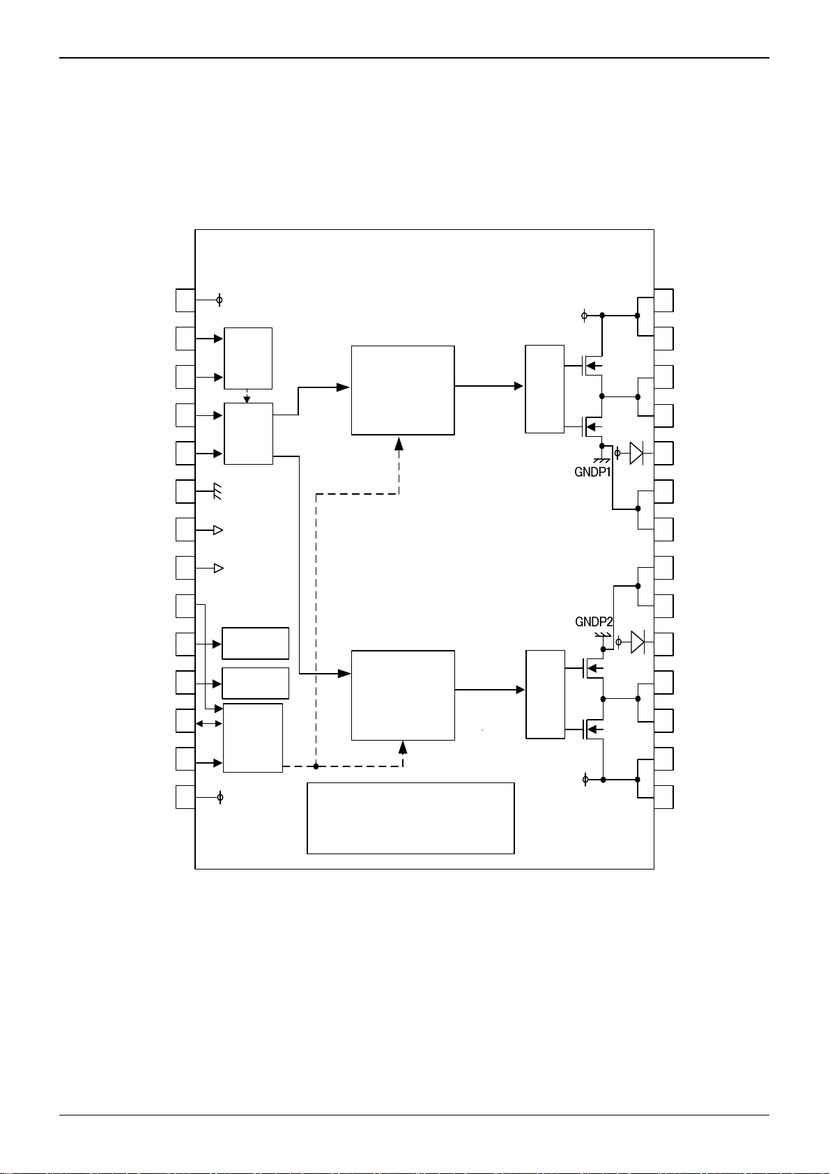
●Pin configuration and Block diagram
1
2
3
4
5
6
7
8
9
10
11
12
13
14
VCCA
Gain
Control
4step
Gain
Amp.
GNDA
FILA
FILP
Power down
Control
Mute
Control
Oscillator
Control
REG_G
PWM
Modulator
PWM
Modulator
High Temperature Protection
Output Short Protection
Under Voltage Protection
Driver
1
Driver
2
VCCP1
VCCP2
Technical Note
28
27
26
25
REG_G
24
23
22
21
20
19
REG_G
18
17
16
15
www.rohm.com
10/31
© 2011 ROHM Co., Ltd. All rights reserved.
2011.10 - Rev.C
 Loading...