

Middle Power Class-D Speaker Amplifiers
Analog Input / BTL Output
Class-D Speaker Amplifier
BD5423AEFS
●Description
BD5423AEFS is a 17W + 17W stereo class-D power amplifier IC, developed for space-saving and low heat-generation
applications such as low-profile TV sets. The IC employs state-of-the-art Bipolar, CMOS, and DMOS (BCD) process
technology that eliminates turn-on resistance in the output power stage and internal loss due to line resistances up to an
ultimate level. With this technology, the IC has achieved high efficiency of 90% (10W + 10W output with 8 load), which is
the top class in the industry. The IC, in addition, employs a compact back-surface heat radiation type power package to
achieve low power consumption and low heat generation and eliminates necessity of installing an external radiator, up to a
total output of 34W. This product satisfies both needs for drastic downsizing, low-profile structures and powerful, highquality playback of the sound system.
●Features
1) A high efficiency of 90% (10W + 10W output with 8 load),
which is the highest grade in the industry and low heat-generation.
2) An output of 17W + 17W (12V, with 4 load) is allowed without an external heat radiator.
3) Driving a lowest rating load of 4 is allowed.
4) Pop noise upon turning power on/off and power interruption has been reduced.
5) High-quality audio muting is implemented by soft-switching technology.
6) An output power limiter function limits excessive output to speakers.
7) High-reliability design provided with built-in protection circuits against high temperatures,
against VCC shorting and GND shorting, against reduced-voltage, and against applying DC voltage to speaker.
8) A master/slave function allowing synchronization of multiple devices reduces beat noises.
9) Adjustment of internal PWM sampling clock frequencies (250kHz to 400kHz)
allows easy protective measures against unwanted radio emission to AM radio band.
10) A compact back-surface heat radiation type power package is employed.
HTSSOP-A44 (5mm × 7.5mm × 1.0mm, pitch 0.8mm )
●Absolute Maximum Ratings
A circuit must be designed and evaluated not to exceed absolute maximum rating in any cases and even momentarily, to
prevent reduction in functional performances and thermal destruction of a semiconductor product and secure useful life and
reliability.
The following values assume Ta =25℃. For latest values, refer to delivery specifications.
Parameter Symbol Ratings
Supply voltage VCC +20 V
Power dissipation Pd
Input voltage for signal pin VIN -0.2 ~ +7.2 V Pin 1, 44 (Note 1)
Unit Conditions
Pin 7, 8, 15, 16, 29, 30, 37, 38, 40
(Note 1, 2)
2.0 W (Note 3)
4.5 W (Note 4)
No.10075EBT02
Input voltage for control pin VCONT -0.2 ~ Vcc+0.2 V Pin 20, 24 (Note 1)
Input voltage for clock pin VOSC -0.2 ~ +7.2 V Pin 23 (Note 1)
Operating temperature range Topr -40 ~ +85 ℃
Storage temperature range Tstg -55 ~ +150 ℃
Maximum junction temperature Tjmax +150 ℃
(Note 1) A voltage that can be applied with reference to GND (pins 11, 12, 33, 34, and 43)
(Note 2) Pd and Tjmax=150℃ must not be exceeded.
(Note 3) 70mm × 70mm × 1.6mm FR4 One-sided glass epoxy board (Back copper foil 0%) installed.
If used under Ta=25℃ or higher, reduce 16mW for increase of every 1℃. The board is provided with thermal via.
(Note 4) 70mm × 70mm × 1.6mm FR4 Both-sided glass epoxy board (Back copper foil 100%) installed.
If used under Ta=25℃ or higher, reduce 36mW for increase of every 1℃. The board is provided with thermal via.
www.rohm.com
© 2010 ROHM Co., Ltd. All rights reserved.
1/17
2010.05 - Rev.B

BD5423AEFS
●Operating Conditions
The following values assume Ta =25℃. Check for latest values in delivery specifications.
Parameter Symbol Ratings Unit Conditions
Technical Note
Supply voltage VCC
Load resistance RL 4 ~ 16 (Note 5)
(Note 5) Pd should not be exceeded.
●Electrical Characteristics
Except otherwise specified T
For latest values, refer to delivery specifications.
Parameter Symbol Limits
Whole circuit
Circuit current 1
(Sampling mode)
Circuit current 2
(Muting mode)
Control circuit
“H” level input voltage VIH 2.3~12 V SDX, MUTEX, MS
“L” level input voltage VIL 0~0.8 V SDX, MUTEX, MS
Audio circuit
Voltage gain GV 28 dB PO = 1W
a = 25℃, VCC = 12V, fIN = 1kHz, Rg = 0, RL = 8、MUTEX="H", MS="L"
ICC1 25 mA With no signal
ICC2 10 mA MUTEX = “L”
+10~+16.5
Unit Conditions
V Pin 7, 8, 15, 16, 29, 30, 37, 38, 40
Maximum output power 1 (Note 6) PO1 10 W THD+N = 10%, RL = 8
Maximum output power 2 (Note 6) PO2 17 W THD+N = 10%, RL = 4
Total harmonic distortion (Note 6) THD 0.1 % PO = 1W, BW=20Hz~20kHz
Crosstalk CT 85 dB PO = 1W, Rg = 0, BW = IHF-A
Output noise voltage
(Sampling mode)
Residual noise voltage
(Muting mode)
Internal sampling clock frequency FOSC 250 kHz MS = “L” (In master operation)
(Note 6) The rated values of items above indicate average performances of the device, which largely depend on circuit layouts, components,
and power supplies. The reference values are those applicable to the device and components directly installed on a board specified by us.
VNO 80 µVrms Rg = 0, BW = IHF-A
VNOM 1 µVrms Rg = 0, BW = IHF-A, MUTEX = “L”
www.rohm.com
© 2010 ROHM Co., Ltd. All rights reserved.
2/17
2010.05 - Rev.B
BD5423AEFS
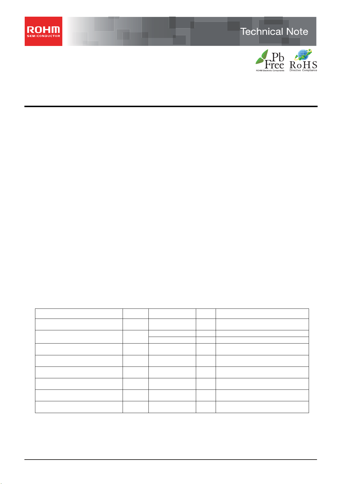
●Electrical characteristic curves (Reference data)
(1) Under Stereo Operation(R
L=8)
100
10
Vcc=12V
=8Ω
R
L
BW=20~20kHz
1
THD+N (%)
6kHz
0.1
0.01
0.001 0.01 0.1 1 10 100
1kHz
100Hz
OUTPUT POWER (W)
Fig. 1 THD+N - Output power Fig. 2 THD+N - Frequency
40
35
30
25
20
15
10
VOLTAGE GAIN (dB)
Vcc=12V
L
=8Ω
R
Po=1W
L=33µH
C=0.47µF
Cg=0.1µF
5
0
10 100 1000 10000 100000
FREQUENCY (Hz)
Fig. 3 Voltage gain - Frequency Fig. 4 Crosstalk - Frequency
-20
-40
0
Vcc=12V
L
=8Ω
R
fin=1kHz
BW=20~20kHz
-60
CROSSTALK (dB)
-80
-100
0.001 0.01 0.1 1 10 100
OUTPUT POWER (W)
Fig. 5 Crosstalk - Output power Fig. 6 Output power - Power supply voltage
Technical Note
100
Vcc=12V
=8Ω
R
L
10
1
THD+N (%)
0.1
0.01
10 100 1000 10000 100000
FREQUENCY (Hz)
0
-20
-40
-60
CROSSTALK (dB)
-80
-100
10 100 1000 10000 100000
FREQUENCY (Hz)
20
RL=8Ω
fin=1kHz
THD=10%
15
10
5
OUTPUT POWER (W)
0
8 1012 141618
VCC (V)
Po=1W
BW=20~20kHz
Vcc=12V
L
=8Ω
R
Po=1W
BW=20~20kHz
THD=1%
www.rohm.com
© 2010 ROHM Co., Ltd. All rights reserved.
3/17
2010.05 - Rev.B
BD5423AEFS
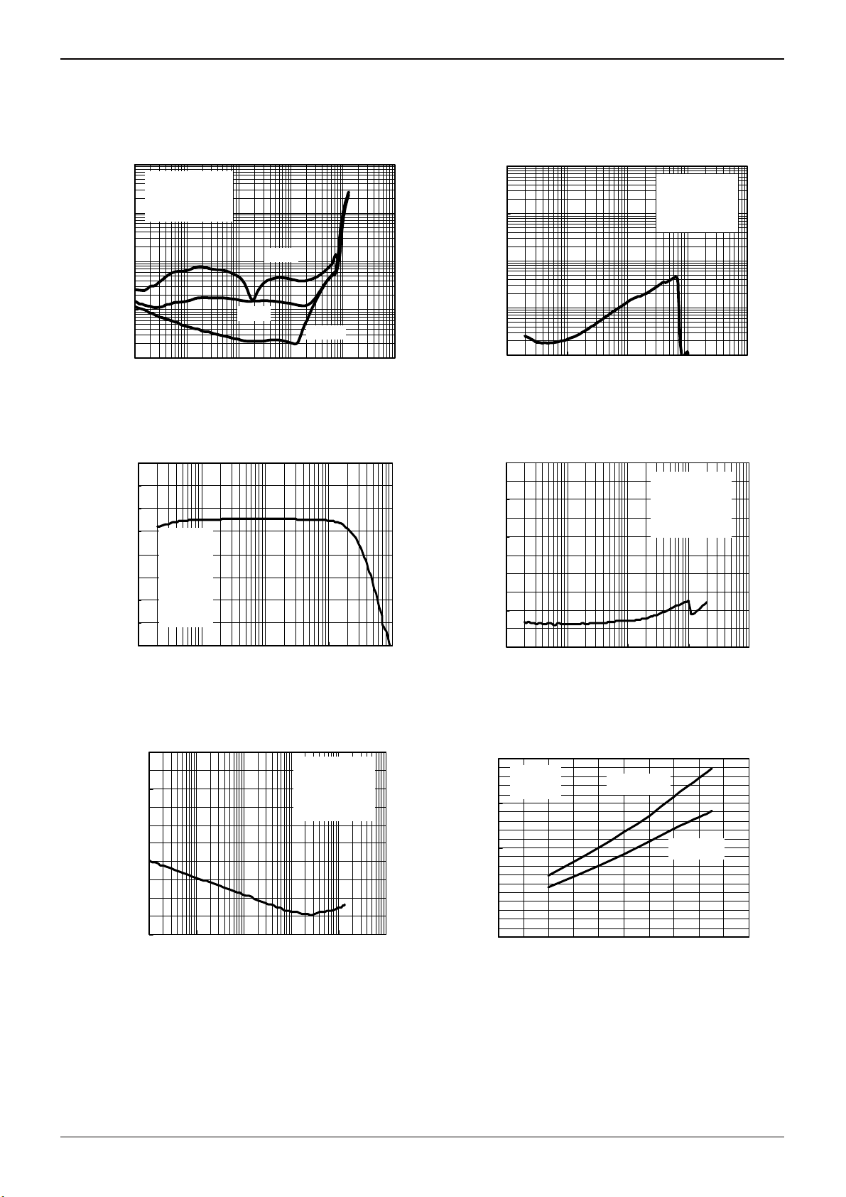
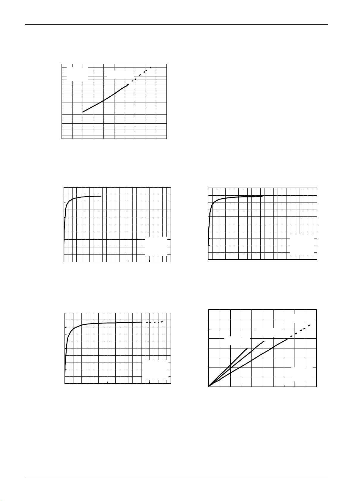
●Electrical characteristic curves (Reference data) – Continued
100
90
80
70
60
50
40
30
EFFICIENCY (%)
20
10
Vcc=10V
L
=8Ω
R
fin=1kHz
0
0 5 10 15 20
OUTPUT POWER (W/ch)
Fig. 7 Efficiency - Output power Fig. 8 Efficiency - Output power
100
90
80
70
60
50
40
30
EFFICIENCY (%)
20
10
Vcc=16.5V
L
R
=8Ω
fin=1kHz
0
0 5 10 15 20
OUTPUT POWER (W/ch)
Fig. 9 Efficiency - Output power Fig. 10 Current consumption - Output power
100
RL=8Ω
RL=8Ω
90
無信号時
80
Without signal
70
60
50
40
ICC (mA)
30
20
10
Sampling
Mute
0
8 1012141618
VCC (V)
Fig. 11 Current consumption - Power supply voltage Fig. 12 FFT of Output Noise Voltage
Technical Note
100
90
80
70
60
50
40
30
EFFICIENCY (%)
20
10
0
0 5 10 15 20
OUTPUT POWER (W/ch)
3
Vcc=12V
2
ICC (A)
1
0
0 5 10 15 20 25 30 35 40
0
-20
-40
-60
-80
-100
NOISE FFT (dBV)
-120
-140
10 100 1000 10000 100000
Vcc=10V
TOTAL OUTPUT POWER (W)
Vcc =12V
Vcc=12V
R
L
=8Ω
R
=8Ω
L
無信号時
Without signal
BW=20~20kHz
BW=20 ~ 20kHz
FREQUENCY (Hz)
Vcc=12V
L
R
=8Ω
fin=1kHz
Vcc=16.5V
RL=8Ω
fin=1kHz
www.rohm.com
© 2010 ROHM Co., Ltd. All rights reserved.
4/17
2010.05 - Rev.B
BD5423AEFS
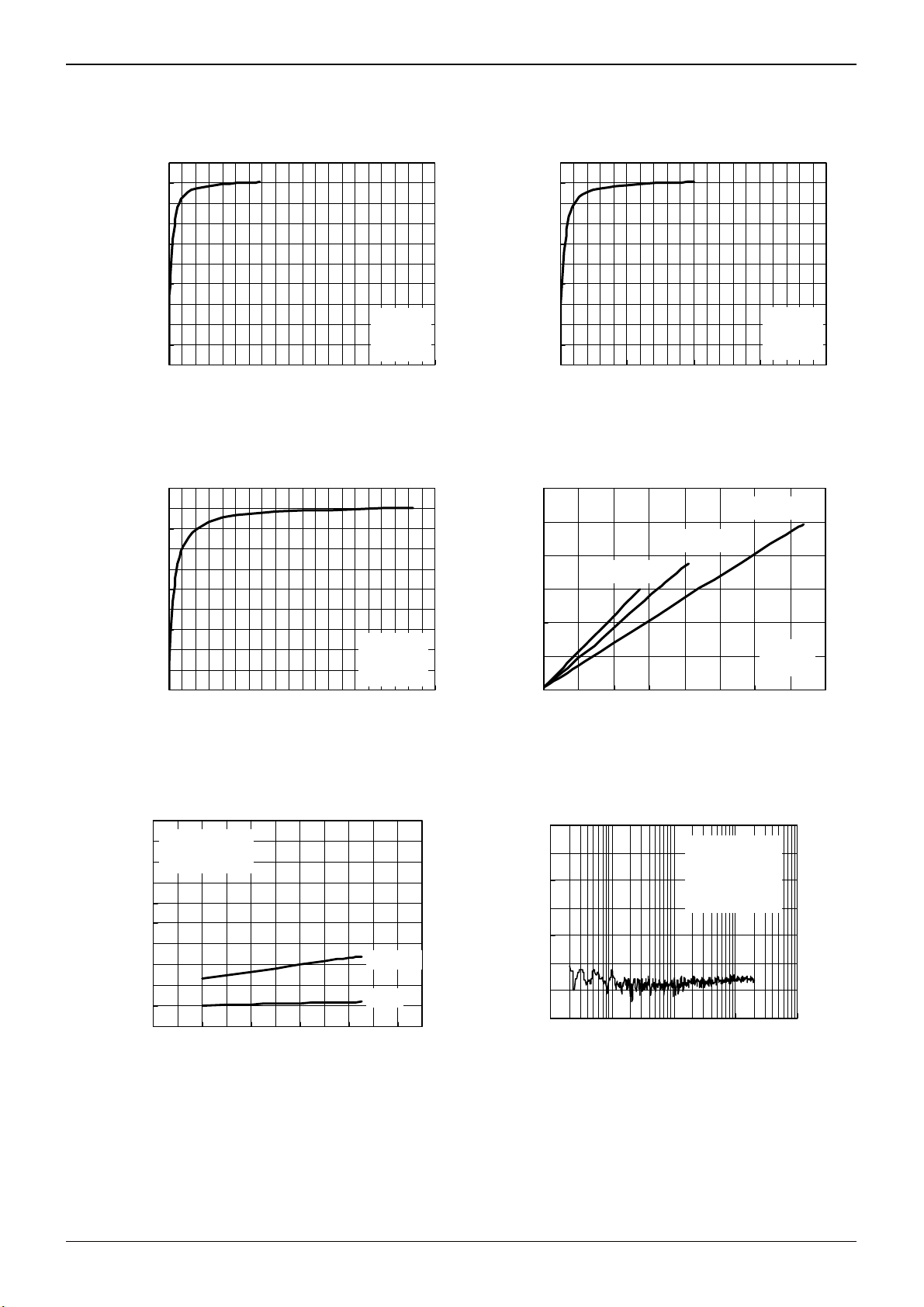
●Electrical characteristic curves (Reference data) – Continued
Technical Note
MUTEX
Pin 20
TM
Pin 26
Speaker
Output
10V/div
5V/div
2V/div
10msec/div
Fig. 13 Wave form when Releasing Soft-mute Fig. 14 Wave form when Activating Soft-mute
VCCA
VHOLD
Pin 27
TM
Pin 26
Speaker
Output
20msec/div
5V/div
5V/div
2V/div
Fig. 15 Wave form on Instantaneous Power Interruption
(20msec / div)
Vcc=12V
=8
R
L
Ω
Po=500mW
fin=500Hz
Vcc=12V
R
=8
L
Ω
Po=500mW
fin=3kHz
M
UTEX
Pin 20
TM
P
in 26
Speaker
Output
VCCA
VHOLD
Pin 27
TM
Pin 26
Speaker
Output
10msec/div
5V/div
5V/div
2msec/div
10V/div
5V/div
2V/div
2V/div
Vcc=12V
R
=8
L
Po=500mW
fin=500Hz
Vcc=12V
R
=8
L
Po=500mW
fin=3kHz
Fig. 16 Wave form on Instantaneous Power Interruption
(2msec / div)
Ω
Ω
Soft Clip
Speaker
Output
Soft Clip
200μsec/div
5V/div
Fig. 17 Wave form on Output Power Limiter function
(Po = 5W)
Vcc=12V
R
=8
L
Ω
Po=5W
THD+n=10%
fin=1kHz
R2=91k
Ω
R3=22k
Ω
www.rohm.com
© 2010 ROHM Co., Ltd. All rights reserved.
5/17
2010.05 - Rev.B
BD5423AEFS
●Electrical characteristic curves (Reference data) – Continued
(2)Under Stereo Operation(R
25
RL=6Ω
fin=1kHz
20
15
10
5
OUTPUT POWER (W)
0
8 1012 141618
Fig. 18 Output power - Power supply voltage
100
90
80
70
60
50
40
30
EFFICIENCY (%)
20
10
0
0 5 10 15 20 25
Fig. 19 Efficiency - Output power Fig. 20 Efficiency - Output power
100
90
80
70
60
50
40
30
EFFICIENCY (%)
20
10
0
0 5 10 15 20 25
Fig. 21 Efficiency - Output power Fig. 22 Current consumption - Output power
Dotted lines of the graphs indicate continuous output power to be obtained on musical signal source or by installing
additional heat sinks.
L=6)
THD=10%
VCC (V)
OUTPUT POWER (W/ch)
OUTPUT POWER (W/ch)
Vcc=10V
L
=6Ω
R
fin=1kHz
Vcc=16.5V
L
R
=6Ω
fin=1kHz
100
90
80
70
60
50
40
30
EFFICIENCY (%)
20
10
0
0 5 10 15 20 25
OUTPUT POWER (W/ch)
4
3
Vcc=12V
Vcc=10V
2
ICC (A)
1
0
0 5 10 15 20 25 30 35 40 45 50
TOTAL OUTPUT POWER (W)
Technical Note
Vcc=12V
L
R
=6Ω
fin=1kHz
Vcc=16.5V
RL=6Ω
fin=1kHz
www.rohm.com
© 2010 ROHM Co., Ltd. All rights reserved.
6/17
2010.05 - Rev.B

BD5423AEFS
●Electrical characteristic curves (Reference data) – Continued
(3) Under Stereo Operation(R
Dotted lines of the graphs indicate continuous output power to be obtained on musical signal source or by installing
additional heat sinks.
30
RL=4Ω
fin=1kHz
25
20
15
10
5
OUTPUT POWER (W)
0
8 1012141618
Fig. 23 Output power - Power supply voltage
100
90
80
70
60
50
40
30
EFFICIENCY (%)
20
10
0
0 5 10 15 20
OUTPUT POWER (W/ch)
Fig. 24 Efficiency - Output power Fig. 25 Efficiency - Output power
100
90
80
70
60
50
40
30
EFFICIENCY (%)
20
10
0
0 5 10 15 20
OUTPUT POWER (W/ch)
Fig. 26 Efficiency - Output power Fig. 27 Current consumption - Output power
L=4Ω)
THD=10%
VCC (V)
Vcc=10V
L
R
=4Ω
fin=1kHz
Vcc=16.5V
L
=4Ω
R
fin=1kHz
100
90
80
70
60
50
40
30
EFFICIENCY (%)
20
10
0
0 5 10 15 20
OUTPUT POWER (W/ch)
4
3
Vcc=10V
2
ICC (A)
1
0
0 5 10 15 20 25 30 35 40
TOTAL OUTPUT POWER (W)
Technical Note
Vcc=12V
L
=4Ω
R
fin=1kHz
Vcc=12V
Vcc=16.5V
RL=4Ω
fin=1kHz
www.rohm.com
© 2010 ROHM Co., Ltd. All rights reserved.
7/17
2010.05 - Rev.B

BD5423AEFS
5
●Pin Assignment
Technical Note
Top View
VCCA
BSP2P
VCCP2P
IN2
44
FIL A
GNDA
43
FIL P
39
40
41
42
VCCP2P
OUT2P
OUT2P
GNDP2
34
35
36
37
38
OUT2N
GNDP2
32
33
VCCP2N
VCCP2N
BSP2N
VHOLD
OUT2N
30
31
28
29
TM
ROSC
27
25
26
MS
24
OSC
23
FIL P
FIL A
GND A
2
1
IN1
PL M T1
VCCA
PW M 2
PW M 1
Limit
Pow er
3
4
5
PL M T3
PL M T2
PL M T4
●Outer Dimensions and Inscriptions
44
BD5423AEFS
0.85
1
1PIN MARK
1.0 MAX
0.8
Fig. 29 Outer Dimensions and Inscriptions of HTSSOP-A44 Package
DRIVER
2P
DRIVER
1P
7
8
6
BSP1P
VCCP1P
9
OUT 1P
VCCP1P
Fig. 28 Pin Assignment Diagram
18.
±
(MAX 18.85 include BURR)
0.1
(6.0)
Ramp
Clock
Control
Generator
Sof t Mute
Pow er- of f
Detector
DRIVER
2N
Under Vol tage Protection
DRIVER
1N
10
11
12
13
14
15
16
OUT 1P
GNDP1
GNDP1
OUT 1N
OUT 1N
VCCP1N
VCCP1N
Protections & Logi c
ERROR
WARNING
17
18
19
BSP1N
ERROR
WARNING
Ou tpu t Shor t Protecti on
High TemperatureProtection
Mute
Output DC Vol tage Protection
Control
N.C.
N.C.
20
21
22
N.C.
N.C.
MUTEX
TYPE
23
(5.0)
22
Lot No.
(Unit: mm)
www.rohm.com
© 2010 ROHM Co., Ltd. All rights reserved.
8/17
2010.05 - Rev.B

BD5423AEFS
●Explanation of Pin Functions (Provided pin voltages are typical values.)
No. Symbol Pin voltage Pin description Internal equalizing circuit
ch1 Analog signal input pin
1
44
2 PLMT1 3.5V
IN1
IN2
3.5V
ch2 Analog signal input pin
Input audio signal via a capacitor.
Voltage-to-current conversion pin for
output power limiter function
Connect a register.
Technical Note
3 PLMT2 -
4 PLMT3 -
5 PLMT4 3.5V
Current-to-voltage conversion pin for
output power limiter function
Connect a register.
Current-to-voltage conversion pin for
output power limiter function
Connect a register.
Bias pin for output power limiter function
Connect a register and a capacitor.
www.rohm.com
© 2010 ROHM Co., Ltd. All rights reserved.
9/17
2010.05 - Rev.B

BD5423AEFS
●Explanation of Pin Functions (continued)
No. Symbol Pin voltage Pin description Internal equalizing circuit
Technical Note
6 BSP1P -
7, 8 VCCP1P Vcc ch1 positive power system power supply pin
9, 10 OUT1P Vcc~0V
11, 12 GNDP1 0V ch1 power system GND pin
13, 14 OUT1N Vcc~0V
15, 16 VCCP1N Vcc ch1 negative power system power supply pin
17 BSP1N -
ch1 positive bootstrap pin
Connect a capacitor.
ch1 positive PWM signal output pin
Connect with output LPF.
ch1 negative PWM signal output pin
Connect with output LPF.
ch1 negative bootstrap pin
Connect a capacitor.
18 WARNING
19 ERROR
H: 5V
L: 0V
H: 5V
L: 0V
Warning output pin
Pin to notify operation warning.
H: Under warning
L: Normal operation
Connect a resister.
Error output pin
A pin for notifying operation errors.
H: Error
L: Normal operation
Connect a resister.
www.rohm.com
© 2010 ROHM Co., Ltd. All rights reserved.
10/17
2010.05 - Rev.B

BD5423AEFS
●Explanation of Pin Functions (continued)
No. Symbol Pin voltage Pin description Internal equalizing circuit
Audio mute control pin
20 MUTEX -
H: Mute off
L: Mute on
Technical Note
21, 22 N.C. -
23 OSC -
24 MS -
N.C. pin
Nothing is connected with IC internal circuit.
Sampling clock signal input/output pin
When using two or more sampling clocks,
connect via a capacitor.
Master/Slave switching pin
Switching of master/slave functions on a
sampling clock signal.
H: Slave operation
L: Master operation
25 ROSC 5.6V
26 TM 0~5V
Internal PWM sampling clock
frequency setting pin
Usually the pin is used open.
To adjust an internal sampling clock
frequency, connect a resister.
Audio muting constant setting pin
Connect a capacitor.
www.rohm.com
© 2010 ROHM Co., Ltd. All rights reserved.
11/17
2010.05 - Rev.B

BD5423AEFS
●Explanation of Pin Functions (continued)
No. Symbol Pin voltage Pin description Internal equalizing circuit
Instantaneous power interruption
detecting voltage setting pin
27 VHOLD 0.68×Vcc
Connect a capacitor.
To adjust a detecting voltage, connect a
resister.
Technical Note
28 BSP2N -
29, 30 VCCP2N Vcc ch2 negative power system power supply pin
31, 32 OUT2N Vcc~0V
33, 34 GNDP2 0V ch2 power system GND pin
35, 36
37, 38 VCCP2P Vcc ch2 positive power system power supply pin
OUT2P Vcc~0V
ch2 negative bootstrap pin
Connect a capacitor.
ch2 negative PWM signal output pin
Connect an output LPF.
ch2 positive PWM signal output pin
Connect an output LPF.
39 BSP2P -
40 VCCA Vcc Analog system power pin
41 FILP
www.rohm.com
© 2010 ROHM Co., Ltd. All rights reserved.
Vcc+35
12
ch2 positive bootstrap pin
Connect a capacitor.
PWM system bias pin
Connect a capacitor.
12/17
2010.05 - Rev.B

BD5423AEFS
●Explanation of Pin Functions (continued)
No. Symbol Pin voltage Pin description Internal equalizing circuit
Analog signal system bias pin
42 FILA 3.5V
Connect a capacitor.
Technical Note
43 GNDA 0V Analog system power supply pin
www.rohm.com
© 2010 ROHM Co., Ltd. All rights reserved.
13/17
2010.05 - Rev.B

BD5423AEFS
●Application Circuit Diagram.
・Vcc=10V~16.5V
Technical Note
C35 C31
ch-2
INPUT
GNDA V CCA
C44
2.2µ F
43
44
GNDA
C43
10µ F
C41
1µ F
C42
10µ F
42
FIL A
C40
0.1µ F
41
FIL P
VCCP
C39
0.68µ F
38
39
40
VCCA
0.22µ F 0.22µ F
L35
15µ H
C38
10µ F
C37 C29
0.1µ F 0.1µ F
35
36
37
DRIVER
2P
Ω
4
SP ch2
C32
1µ F
SL AV E
MASTER
L31
15µ H
GNDD
GND P
C28
0.68µ F
C27
3.3µ F
0.1µ F
C26
OPEN
28
30
31
32
33
34
DRIVER
2N
29
27
Pow er- of f
Detector
25
26
Ramp
Generator
Sof t M ut e
CLK I/O
C23
0.1µ F
24
23
Clock
Control
PW M 2
PW M 1
Under Vol tage Protecti on
DRIVER
1P
Pow er
Limit
2
3
4
R3
Ω
0.1µ F
22k
5
R4
Ω
C5
GNDA
1
Ω
R2
22k
22k
GNDA
C1
2.2µF
ch-1
INPUT
6
C6
0.68µ F
VCCP
7
8
9
10
C7
0.1µ F
C8
10µ F
L9
15µ H
C9
0.22µ F
11
12
C13
0.22µ F
C10
1µ F
DRIVER
1N
13
GNDP
14
C15
0.1µ F
L13
15µ H
15
16
C17
0.68µ F
Protecti ons & L ogic
ERROR
WARNING
17
18
19
R18
100kΩ100k
ERROR OUTPUT
WARNING OUTPUT
Output Short Protection
H ig h T emper atur e Pr ot ec ti on
Ω
R19
Output DC Vol tage Protection
Mute
Control
N.C.
N.C.
20
21
22
N.C.
N.C.
MUTE
Fig. 30 Circuit diagram under stereo operation with 4- load
www.rohm.com
© 2010 ROHM Co., Ltd. All rights reserved.
SP ch1
14/17
Ω
4
2010.05 - Rev.B

BD5423AEFS
Technical Note
Table 1 BOM list for stereo operation with 4- load
No. Item Part Number Vendor
1 IC BD5423AEFS ROHM HTSSOP-A44 - - - - 1 IC1
2 C GRM219B31E684KA88D MURATA 2012 0805 0.68µF 25V ±10% ±10% 4 C6, C17, C28, C39
3 C GRM188R11H104KA93 MURATA 1608 0603 0.1µF 50V ±10% ±10% 5 C7, C15, C29, C37, C40
4 C GRM31MB11H224KA01 MURATA 3216 1206 0.22µF 50V ±10% ±10% 4 C9, C13, C31, C35
5 C 25ST225M3216 Rubycon 3225 1210 2.2µF 25V ±20% ±5% 2 C1, C44
6 C 50ST105M3225 Rubycon 3225 1210 1µF 50V ±20% ±5% 2 C10, C32
7 C GRM21BB31E335KA75 MURATA 2012 0805 3.3µF 25V ±10% ±10% 1 C27
8 C GRM188B11E104KA MURATA 1608 0603 0.1µF 25V ±10% ±10% 3 C5, C23, C26
9 C GRM21BB11C105KA MURATA 2012 0805 1µF 16V ±10% ±10% 1 C41
10 C GRM21BB31C106KE15 MURATA 2012 0805 10µF 16V ±10% ±10% 1 C42
11 C 25SVPD10M SANYO 6666 2626 10µF 25V ±20% ±25% 3 C8, C38, C43
12 R MCR01MZPF2202 ROHM 1005 0402 22k 50V ±1% ±200ppm/℃ 3 R2, R3, R4
13 R MCR01MZPF1003 ROHM 1005 0402 100k 50V ±1% ±200ppm/℃ 2 R18, R19
No. Item Part Number Vendor
14 L 7G09B-150M SAGAMI 10×9×10 15µH×2 ±20% 44mmax. 4.1A max. 2 L9, L13, L31, L35
Configuration
mm inch
Configuration
mm
Val ue
Value Tolerance
Rated
voltage
Tolerance
Resistance
DC
Temperature
characteristics
Rated
DC Current
Quantity Reference
Quantity Reference
www.rohm.com
© 2010 ROHM Co., Ltd. All rights reserved.
15/17
2010.05 - Rev.B

BD5423AEFS
Technical Note
●Notes for use
1. About absolute maximum ratings
If an applied voltage or an operating temperature exceeds an absolute maximum rating, it may cause destruction of a
device. A result of destruction, whether it is short mode or open mode, is not predictable. Therefore, provide a physical
safety measure such as fuse, against a special mode that may violate conditions of absolute maximum ratings.
2. About power supply line
As return of current regenerated by back EMF of output coil happens, take steps such as putting capacitor between
power supply and GND as a electric pathway for the regenerated current. Be sure that there is no problem with each
property such as emptied capacity at lower temperature regarding electrolytic capacitor to decide capacity value. If the
connected power supply does not have sufficient current absorption capacity, regenerative current will cause the voltage
on the power supply line to rise, which combined with the product and its peripheral circuitry may exceed the absolute
maximum ratings. It is recommended to implement a physical safety measure such as the insertion of a voltage clamp
diode between the power supply and GND pins.
3. Potential of GND (11, 12, 33, 34, and 43 pins)
Potential of the GND terminal must be the lowest under any operating conditions.
4. About thermal design
Perform thermal design with sufficient margins, in consideration of maximum power dissipation Pd under actual operating
conditions. This product has an exposed frame on the back of the package, and it is assumed that the frame is used with
measures to improve efficiency of heat dissipation. In addition to front surface of board, provide a heat dissipation pattern
as widely as possible on the back also.
A class-D power amplifier has heat dissipation efficiency far higher than that of conventional analog power amplifier and
generates less heat. However, extra attention must be paid in thermal design so that a power dissipation Pdiss should not
exceed the maximum power dissipation Pd.
Maximum power dissipation
Power dissipation
jmax
Pd
aj
1
PP Odiss
W
W 1-
Tjmax: Maximum temperature junction = 150[℃]
Ta: Operating ambient temperature [℃]
θja: Package thermal resistance [℃/W]
Po: Output power [W]
η: Efficiency
Ta-T
5. About operations in strong electric field
Note that the device may malfunction in a strong electric field.
6. Thermal shutdown (TSD) circuit
This product is provided with a built-in thermal shutdown circuit. When the thermal shutdown circuit operates, the output
transistors are placed under open status. The thermal shutdown circuit is primarily intended to shut down the IC avoiding
thermal runaway under abnormal conditions with a chip temperature exceeding Tjmax = 150℃, and is not intended to
protect and secure an electrical appliance. Accordingly, do not use this circuit function to protect a customer's electrical
appliance.
7. About shorting between pins and installation failure
Be careful about direction and displacement of an LSI when installing it onto the board. Faulty installation may destroy
the LSI when the device is energized. In addition, a foreign matter getting in between LSI pins, pins and power supply,
and pins and GND may cause shorting and destruction of the LSI.
8. About power supply startup and shutdown
When starting up a power supply, be sure to place the MUTEX pin (pin 20) at “L” level. When shutting down a power
supply also, be sure to place the pin at “L” level. Those processes reduce pop noises generated upon turning on and off
the power supply. In addition, all power supply pins must be started up and shut down at the same time.
9. About WARNING output pin (pin 18) and ERROR output pin (pin 19)
A WARNING flag is output from the WARNING output pin upon operation of the high-temperature protection function and
under-voltage protection function. And an ERROR flag is output from the ERROR output pin upon operation of VCC/GND
shorting protection function and speaker DC voltage applying protection function. These flags are the function which the
condition of this product is shown in. The use which aimed at the protection except for this product is prohibition.
10. About N.C. pins (pins 21 and 22)
The N.C. (Non connection) pins are not connected with an internal circuit. Leave the pins open or connect them to GND.
www.rohm.com
© 2010 ROHM Co., Ltd. All rights reserved.
16/17
2010.05 - Rev.B

BD5423AEFS
●Ordering part number
Technical Note
B D
Part No.
HTSSOP-A44
44 23
9.5±0.2
7.5±0.1
1
0.85
1.0MAX
0.85±0.05
0.08±0.05
5 4 2 3 A E F S
Part No.
18.5±0.1
(MAX 18.85 include BURR)
(6.0)
1PIN MARK
0.8
0.37
+0.05
-
0.04
22
0.08
0.08
(5.0)
S
4°
S
M
+
6°
−
4°
0.5±0.15
1.0±0.2
+0.05
0.17
-
0.03
(Unit : mm)
Package
EFS:HTSSOP-44
<Tape and Reel information>
Embossed carrier tape (with dry pack)Tape
Quantity
Direction
of feed
1500pcs
E2
The direction is the 1pin of product is at the upper left when you hold
()
reel on the left hand and you pull out the tape on the right hand
Reel
-E 2
Packaging and forming specification
E2: Embossed tape and reel
1pin
Order quantity needs to be multiple of the minimum quantity.
∗
Direction of feed
www.rohm.com
© 2010 ROHM Co., Ltd. All rights reserved.
17/17
2010.05 - Rev.B

Notes
No copying or reproduction of this document, in part or in whole, is permitted without the
consent of ROHM Co.,Ltd.
The content specied herein is subject to change for improvement without notice.
The content specied herein is for the purpose of introducing ROHM's products (hereinafter
"Products"). If you wish to use any such Product, please be sure to refer to the specications,
which can be obtained from ROHM upon request.
Examples of application circuits, circuit constants and any other information contained herein
illustrate the standard usage and operations of the Products. The peripheral conditions must
be taken into account when designing circuits for mass production.
Great care was taken in ensuring the accuracy of the information specied in this document.
However, should you incur any damage arising from any inaccuracy or misprint of such
information, ROHM shall bear no responsibility for such damage.
The technical information specied herein is intended only to show the typical functions of and
examples of application circuits for the Products. ROHM does not grant you, explicitly or
implicitly, any license to use or exercise intellectual property or other rights held by ROHM and
other parties. ROHM shall bear no responsibility whatsoever for any dispute arising from the
use of such technical information.
Notice
The Products specied in this document are intended to be used with general-use electronic
equipment or devices (such as audio visual equipment, ofce-automation equipment, communication devices, electronic appliances and amusement devices).
The Products specied in this document are not designed to be radiation tolerant.
While ROHM always makes effor ts to enhance the quality and reliability of its Products, a
Product may fail or malfunction for a variety of reasons.
Please be sure to implement in your equipment using the Products safety measures to guard
against the possibility of physical injury, re or any other damage caused in the event of the
failure of any Product, such as derating, redundancy, re control and fail-safe designs. ROHM
shall bear no responsibility whatsoever for your use of any Product outside of the prescribed
scope or not in accordance with the instruction manual.
The Products are not designed or manufactured to be used with any equipment, device or
system which requires an extremely high level of reliability the failure or malfunction of which
may result in a direct threat to human life or create a risk of human injury (such as a medical
instrument, transportation equipment, aerospace machinery, nuclear-reactor controller, fuelcontroller or other safety device). ROHM shall bear no responsibility in any way for use of any
of the Products for the above special purposes. If a Product is intended to be used for any
such special purpose, please contact a ROHM sales representative before purchasing.
If you intend to export or ship overseas any Product or technology specied herein that may
be controlled under the Foreign Exchange and the Foreign Trade Law, you will be required to
obtain a license or permit under the Law.
Thank you for your accessing to ROHM product informations.
More detail product informations and catalogs are available, please contact us.
ROHM Customer Support System
www.rohm.com
© 2010 ROHM Co., Ltd. All rights reserved.
http://www.rohm.com/contact/
R1010
A
 Loading...