


Middle Power Class-D Speaker Amplifiers
Analog Input / BTL Output
Class-D Speaker Amplifier
BD5413EFV
●Description
BD5413EFV is a 5W + 5W stereo class-D power amplifier specifically developed for low power consumption and low heat
generation applications like powered speakers. BD5413EFV employs the state-of-the-art BCD (Bipolar, CMOS and DMOS)
process technology to eliminate a turn-on resistance in the output power stage and an internal loss due to a wiring
resistance as much as possible, achieving a high performance of 80% (4W + 4W output with a load resistance of 8Ω). In
addition, BD5413EFV employs a compact power package which dissipates heat via the rear to achieve low power
consumption and low heat generation so that the need for connecting an external heat radiator can be eliminated up to a
total output of 12.8W. This product meets the needs for compact, thin sound generation systems and powerful, high-quality
sound reproduction.
●Features
1) Small output noise voltage capable of achieving a high S/N set
Input conversion noise voltage = 2.8μVrms
A bipolar differential is used for input amplifier to eliminate 1/f noise.
2) Support of power supply voltage ranging from 6V to 10.5V
A supply voltage range is supported that matches an AC adaptor or battery cell driven set.
When a set is battery driven, its operating time can be extended by means of a high performance class-D amplifier.
3) Support of low current consumption mode
A circuit current in shut-down mode is 1μA or less.
4) Built-in soft muting function for reducing pop at shut-down ON or OFF
When a signal is present, its smooth envelope waveform is realized owing to this function.
In addition, when no signal is present, pop generation is eliminated.
A transit time can be adjusted easily through the use of an external capacitor.
5) Realization of high efficiency and low heat generation
Efficiency = 80% (4W+4W (Vcc=9V, R
A compact power package HTSSOP-B24 (7.8mm x 7.6mm) is employed.
6) Built-in function for reducing pop generation at disconnection from the outlet
7) Support of function for sampling frequency selection
An internal PWM sampling frequency can be selected from three frequencies (200kHz, 250kHz and 300kHz).
Countermeasures against interference (beat noise) due to a switching power source can be taken as needed.
8) Realization of high reliability
Countermeasures against short-circuits due to output terminals shorted to V
(support of automatic recovery).
A temperature protection circuit is incorporated (support of automatic recovery).
9) Support of ERROR pin
ERROR output takes place as a warning which indicates an error.
(short-circuits due to output terminals shorted to V
=8Ω) output can be made without using an external heat radiator.)
L
or ground can be taken
CC
or ground, or IC high temperature abnormality).
CC
No.10075EBT01
www.rohm.com
© 2010 ROHM Co., Ltd. All rights reserved.
1/14
2010.05 - Rev.B
BD5413EFV
Technical Note
●Absolute maximum ratings
A circuit must be designed and evaluated not to exceed absolute maximum rating in any cases and even momentarily, to
prevent reduction in functional performances and thermal destruction of a semiconductor product and secure useful life and
reliability.
The following values assume Ta =25℃. For latest values, refer to delivery specifications.
Parameter
Symbol Ratings Unit Conditions
Supply voltage VCC +15 V Pin 3, 5, 10, 12, 16, 21 (Note 1,2)
Power dissipation Pd
1.1 W (Note 3)
2.8 W (Note 4)
Input voltage for signal pin VIN -0.2 to Vcc+0.2 V Pin 23, 24 (Note 1)
Input voltage for control pin VCONT -0.2 to Vcc+0.2 V Pin 14, 15 (Note 1)
Operating temperature range Topr -40 to +85 ℃
Storage temperature range Ts tg -55 to +150 ℃
Maximum junction temperature Tjmax +150 ℃
(Note 1) A voltage that can be applied with reference to GND (pins 1, 7, 8, 13, 18 and 19)
(Note 2) Pd and Tjmax=150℃ must not be exceeded.
(Note 3) 70mm × 70mm × 1.6mm FR4 One-sided glass epoxy board (Back copper foil 0%) installed.
If used under Ta=25℃ or higher, reduce 8.8 mW for increase of every 1℃. The board is provided with thermal via.
(Note 4) 70mm × 70mm × 1.6mm FR4 Both-sided glass epoxy board (Back copper foil 100%) installed.
If used under Ta=25℃ or higher, reduce 22.4 mW for increase of every 1℃. The board is provided with thermal via.
●Operating conditions
The temperature (Ta) is 25℃. For the latest temperature, refer to the delivery specifications.
Parameter Symbol Ratings Unit Conditions
Supply voltage VCC +6 to +10.5 V Pin 3, 5, 10, 12, 16, 21
Load resistance RL 6 to 16 Ω (Note 5)
(Note 5) This value must not exceed Pd.
●Electrical characteristics
Unless otherwise stated, Ta=25℃, Vcc=9V, f
IN=1kHz, Rg=0Ω, RL=8Ω, SDX="H" and FC="M (OPEN)"
are assumed. For the latest values, refer to the delivery specifications.
Parameter Symbol Limits Unit Conditions
Whole circuit
Circuit current 1 (sampling mode) ICC1 12 mA No signal, no load
Circuit current 2 (mute mode) ICC2 1 µA SDX = “L”
Control
Input voltage with SDX pin set to "H" VIHSDX 2.5 to 9 V Sampling state
Input voltage with SDX pin set to "L" VILSDX 0 to 0.5 V Shut-down state
Input voltage with FC pin set to "H" VIHFC 8.2 to 9 V Setting of Fs=300kHz
Input voltage with FC pin set to "M" VIMFC 3.8 to 5.2 V Setting of Fs=250kHz
Input voltage with FC pin set to "L" VILFC 0 to 0.8 V Setting of Fs=200kHz
Audio output
Voltage gain GV 30 dB PO = 1W
Maximum output power 1 (Note 6) PO1 4 W THD+N = 10%, RL = 8Ω
Maximum output power 2 (Note 6) PO2 5 W THD+N = 10%, RL = 6Ω
Total harmonic distortion ratio (Note 6) THD 0.2 % PO = 1W, BW=20Hz to 20kHz
Crosstalk CT 65 dB PO = 1W, Rg = 0Ω, BW = IHF-A
Output noise voltage (sampling mode) VNO 90 µVrms Rg = 0Ω, BW = IHF-A
Residual noise voltage (mute mode) VNOM 1 µVrms Rg = 0Ω, BW = IHF-A, MUTEX = “L”
200
Internal sampling clock frequency FS
250
kHz
300
(Note 6) The rated values of items above indicate average performances of the device, which largely depend on circuit layouts, components,
and power supplies. The reference values are those applicable to the device and components directly installed on a board specified by us.
FC = L
FC = M(OPEN)
FC = H
www.rohm.com
© 2010 ROHM Co., Ltd. All rights reserved.
2/14
2010.05 - Rev.B
BD5413EFV
r
r
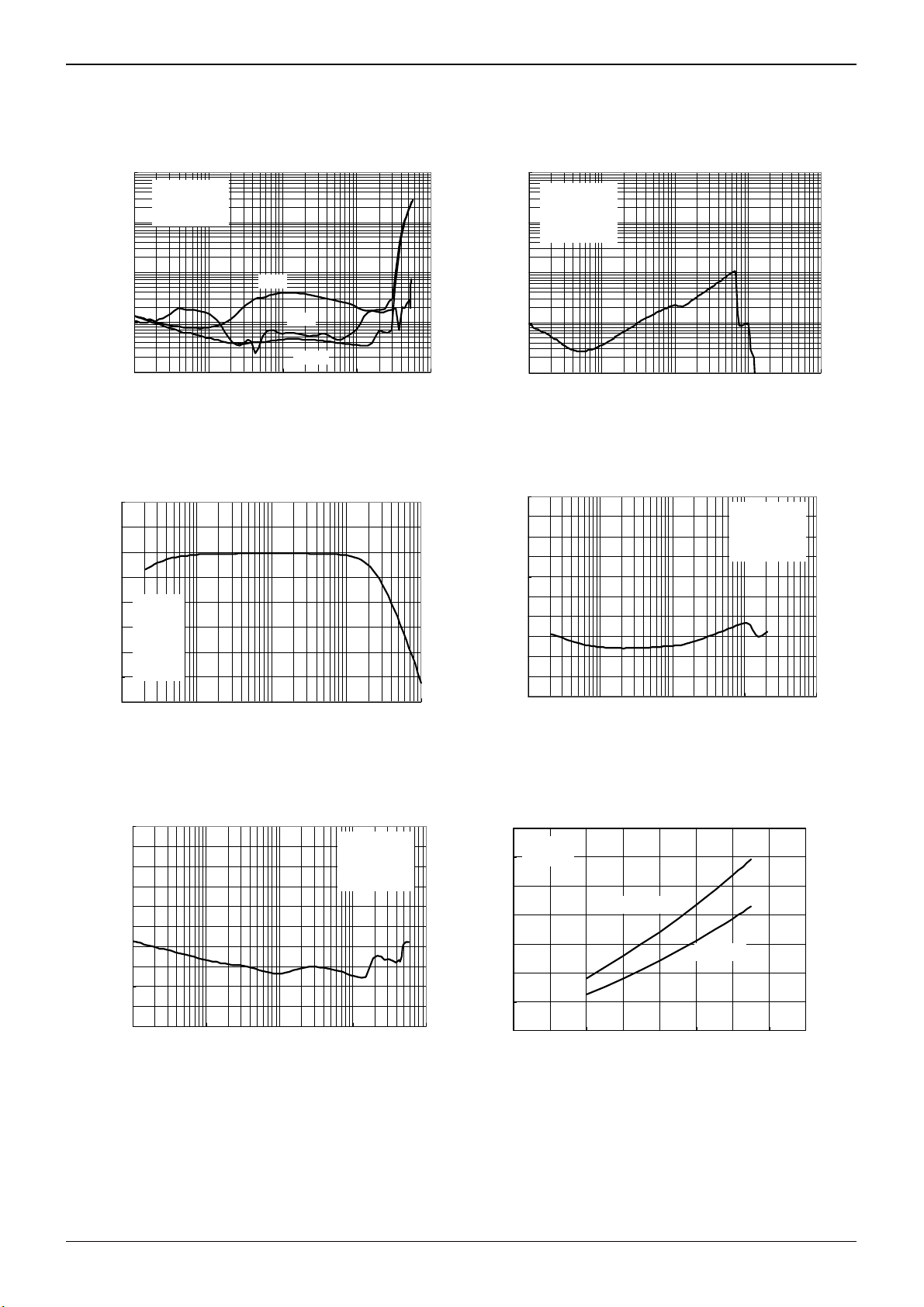
●Electrical characteristic curves (Ta=25℃) (Reference data)
(1) Under Stereo Operation (R
L=8Ω)
Technical Note
100
Vcc=9V
=8Ω
R
L
BW=20~20kHz
10
1
THD+N (%)
0.1
0.01
0.001 0.01 0.1 1 10
6kHz
1kHz
100Hz
OUTPUT POWER (W)
Fig. 1 THD+N - Output Powe
40
35
30
25
20
Vcc=9V
=8Ω
R
L
15
Po=1W
L=33µH
VOLTAGE GAIN (dB)
10
C=0.47µF
Cg=0.1µF
5
0
10 100 1000 10000 100000
FREQUENCY (Hz)
Fig. 3 Voltage Gain - Frequency Fig. 4 Crosstalk - Frequency
100
Vcc=9V
=8Ω
R
L
Po=1W
10
BW=20~20kHz
1
THD+N (%)
0.1
0.01
10 100 1000 10000 100000
FREQUENCY (Hz)
Fig. 2 THD+N - Frequency
0
-20
-40
-60
CROSSTALK (dB)
-80
-100
10 100 1000 10000 100000
FREQUENCY (Hz)
Vcc=9V
=8Ω
R
L
Po=1 W
BW=20~20kHz
0
-20
-40
-60
CROSSTALK (dB)
-80
-100
0.001 0.01 0.1 1 10
OUTPUT POWER (W)
Fig. 5 Crosstalk - Output Powe
www.rohm.com
© 2010 ROHM Co., Ltd. All rights reserved.
Vcc=12V
R
=8Ω
L
fin=1kHz
BW=20~20kHz
3/14
14
RL=8Ω
12
fin=1kHz
10
8
6
THD=10%
THD=1%
4
OUTPUT POWER (W)
2
0
456789101112
VCC (V)
Fig. 6 Output Power - Supply Voltage
2010.05 - Rev.B
BD5413EFV
V
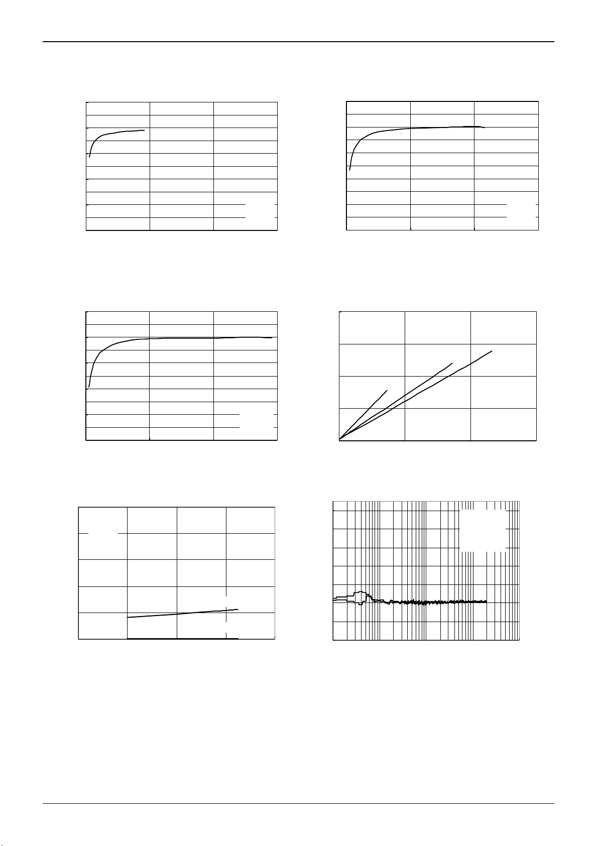
●Electrical characteristic curves (Reference data) – Continued
Technical Note
100
90
80
70
60
50
40
EFFICIENCY (% )
30
20
10
0
0246
OUTPUT POWER (W/ch)
Vcc=6V
R
=8Ω
L
fin=1kHz
100
90
80
70
60
50
40
EFFICIENCY (% )
30
20
10
0
0246
OUTPUT POWER (W/ch)
Vcc=9V
R
=8Ω
L
fin=1kHz
Fig. 7 Efficiency - Output Power Fig. 8 Efficiency - Output Power
100
90
80
70
60
50
40
EFFICIENCY (% )
30
20
10
0
0246
OUTPUT POWER (W/ch)
Vcc=10.5V
R
=8Ω
L
fin=1kHz
2
Vcc=9V Vcc=10.5
1
ICC (A)
Vcc=6V
RL=8Ω
fin=1kHz
0
051015
TOTAL OUTPUT POWER (W)
Fig. 9 Efficiency - Output Power Fig. 10 Current Consumption - Output Power
50
RL=8Ω
No signal
40
30
20
ICC(mA)
Sampling
10
ShutDown
0
4681012
VCC(V)
Fig. 11 50 Current Consumption - Supply Voltage Fig. 12 Output Noise Voltage FFT
-10
-30
-50
-70
-90
-110
NOISE FFT (dBV)
-130
-150
10 100 1000 10000 100000
FREQUENCY (Hz)
Vcc=9V
RL=8Ω
No signal
Gain=29.6dB
www.rohm.com
© 2010 ROHM Co., Ltd. All rights reserved.
4/14
2010.05 - Rev.B
BD5413EFV
●Electrical characteristic curves (Reference data) – Continued
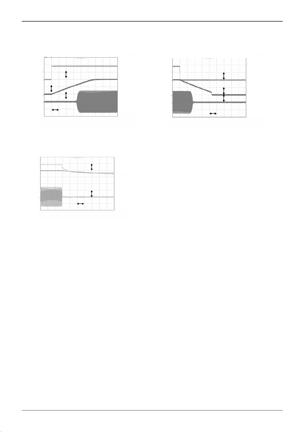
Technical Note
SDX
Pin14
TS
Pin22
Speaker
Output
2V/div
200msec/ div
5V/div
2V/div
Vcc=9V
L
R
Ω
=8
Po=500mW
fin=100Hz
SDX
Pin14
TS
Pin22
Speaker
Output
5V/div
2V/div
2V/div
200msec/ div
Vcc=9V
L
R
Ω
=8
Po=500mW
fin=100Hz
Fig. 13 Waveform at Soft Mute Reset Fig. 14 Waveform at Soft Mute
VCCA
FIL
Pin2
Speaker
Output
5V/div
2V/div
20msec/div
Vcc=9V
L
R
=8Ω
Po=500mW
fin=1kHz
Fig. 15 Waveform at Instantaneous Power
Interruption (20msec/div)
www.rohm.com
© 2010 ROHM Co., Ltd. All rights reserved.
5/14
2010.05 - Rev.B

BD5413EFV
●Electrical characteristic curves (Reference data) – Continued
THD=10%
VCC (V)
L=16 Ω)
Vcc=6V
R
=8Ω
L
fin=1kHz
(2) Under Stereo Operation (R
100
10
RL=16Ω
90
fin=1kHz
80
8
70
6
60
50
4
40
EFFICIENCY (% )
30
OUTPUT POW ER (W)
2
20
10
0
0
4681012
0246
OUTPUT POWER (W/ch)
Fig. 16 Output Power - Supply Voltage Fig. 17 Efficiency - Output Power
Technical Note
100
90
80
70
60
50
40
EFFICIENC Y (% )
30
20
10
0
024
OUTPUT POWER (W/c h)
Vcc=6V
R
=16Ω
L
fin=1kHz
100
90
80
70
60
50
40
EFFICIENC Y (% )
30
20
10
0
024
OUTPUT POWER (W/ch)
Vcc=9V
=16Ω
R
L
fin=1kHz
100
90
80
70
60
50
40
EFFICIENC Y (% )
30
20
10
0
024
Fig. 18 Efficiency - Output Power Fig. 19 Efficiency - Output Power
2
1.5
1
ICC(A)
0.5
0
02468
Vcc=6V
TOTAL OUTPUT POWER (W)
Vcc=9V
Vcc=10.5V
RL=16
Ω
fin=1kHz
Fig. 20 Current Consumption - Output Power
OUTPUT POWER (W/ch)
Vcc=10.5V
R
=16Ω
L
fin=1kHz
www.rohm.com
© 2010 ROHM Co., Ltd. All rights reserved.
6/14
2010.05 - Rev.B

BD5413EFV
V
●Electrical characteristic curves (Reference data) – Continued
(3) Under Stereo Operation (R
L=6Ω)
Technical Note
100
90
80
70
60
50
40
EFFICIENC Y (% )
30
20
10
0
0246
OUTPUT POWER (W/ch)
Fig. 21 Output Power - Supply Voltage Fig. 22 Efficiency - Output Power
RL=6Ω
14
fin=1kHz
12
10
8
6
4
OUTPUT POW ER (W)
2
0
4681012
THD=10%
Fig. 23 Efficiency - Output Power Fig. 24 Efficiency - Output Power
100
90
80
70
60
50
40
EFFICIENCY (%)
Vcc=9V
R
=6Ω
L
fin=1kHz
30
20
10
0
0246
OUTPUT POWER (W/ch)
Vcc=10.5V
R
=6Ω
L
fin=1kHz
100
90
80
70
60
50
40
EFFICIENC Y (% )
VCC (V)
30
20
10
0
0246
OUTPUT POWER (W/ch)
Vcc=6V
R
=6Ω
L
fin=1kHz
2
Vcc=9V
1
ICC (A)
0
Vcc=6V
051015
TOTAL OUTPUT POWER (W)
Fig. 25 Current Consumption - Output Power
www.rohm.com
© 2010 ROHM Co., Ltd. All rights reserved.
Vcc=10.5
RL=6Ω
fin=1kHz
7/14
2010.05 - Rev.B

BD5413EFV
●Pin Assignment Diagram
Technical Note
Top View
1
GNDA
2
FIL
VCCA
3
4
TEST
VCCP1P
OUT1P
GNDP1
GNDP1
OUT1N
VCCP1N
ERR
VCCD
5
6
7
8
9
10
11
12
●Outer Dimensions and Inscriptions
(Maximum size including burr: 6.15) (5.0)
Fig. 27 Outer Dimensions and Inscriptions of the HTSSOP-B24 Package
FIL
N.C .
DRIVER
1P
DRIVER
1N
ERROR
High Temperature Protection
Fig. 26 Pin Assignment
D5413EFV
PWM1
Protections & Logic
Power - off Detector
Output Short Protection
PWM2
Soft
Shutdown
DRIVER
2P
DRIVER
2N
Sampling
Frequency
Control
Shutdown
Control
Type
Lot No.
24
23
22
21
20
19
18
17
16
15
14
13
IN1
IN2
TS
VCCP 2P
OUT 2P
GNDP 2
GNDP 2
OUT2N
VCCP 2N
FC
SDX
GNDD
www.rohm.com
© 2010 ROHM Co., Ltd. All rights reserved.
8/14
2010.05 - Rev.B

BD5413EFV
●Pin configuration (Pin Voltage: Typical Value)
No. Symbol Pin voltage Pin description Internal equalizing circuit
3
ch1: Analog signal input pin
24
23
IN1
IN2
1/2V
CC
ch2: Analog signal input pin
23/2 4
20
k
Input an audio signal via a capacitor.
Technical Note
5 VCCP1P Vcc ch1: Positive power system power supply pin
6 OUT1P Vcc to 0V
ch1: Positive PWM signal output pin
Make connection to the output LPF.
7, 8 GNDP1 0V ch1: Power GND pin
9 OUT1N Vcc to 0V
ch1: Negative PWM signal output pin
Make connection to the output LPF.
10 VCCP1N Vcc ch1: Negative power system power supply pin
Error output pin
Pin for notifying an operation error
H: Error
11 ERROR
H: 5V
L: 0V
L: Normal operation
1
12
11
7 , 8
7 , 8
5
6
10
9
100
ON /OFF
300k
12 VCCD VCC Control power supply pin
13 GNDD 0V Control GND pin
Shut-down control pin
14 SDX -
H: Shut-down OFF
L: Shut-down ON
www.rohm.com
© 2010 ROHM Co., Ltd. All rights reserved.
9/14
13
12
225k
14
13
175k
2010.05 - Rev.B

BD5413EFV
●Pin configuration - Continued
No. Symbol Pin voltage Pin description
Technical Note
Internal equalizing circuit
4 TEST VCC
Keep this pin open or connect it to VCC for
regular use.
Shut-down ON/OFF
Do not use the TEST pin.
22 TS 0 to 4V
Constant setting pin
Connect a capacitor.
16 VCCP2N Vcc ch2: Negative power system power supply pin
17 OUT2N Vcc to 0V
18,
GNDP2 0V ch2: Power GND pin
19
ch2: Negative PWM signal output pin
Make connection to the output LPF.
12
22
13
18 , 19
100
16
17
21
20 OUT2P Vcc to 0V
ch2: Positive PWM signal output pin
Make connection to the output LPF.
21 VCCP2P Vcc ch2: Positive power system power supply pin
3 VCCA Vcc Analog system power supply pin
Analog signal system bias pin
2 FILA 1/2VCC
Connect a capacitor.
1 GNDA 0V Analog signal system GND pin
18 , 19
20
3
2
1
www.rohm.com
© 2010 ROHM Co., Ltd. All rights reserved.
10/14
2010.05 - Rev.B

BD5413EFV
●Application Circuit Diagram
(1)Application Circuit Diagram with a Load of 8Ω for Stereo Operation
・Vcc=6V to 10.5V
SP ch1
(8Ω)
GNDA
C7
0.47µ
VCC
C2
10µ
33µH
C6
0.1µ
C8
0.1µ
33µH
L1
L2
C1
47µ
VCCP1
10µ
+
GNDP1
C3
0.1µ
C9
0.1µ
C4C5
0.1µ
1
FIL
2
3
TEST
4
PWM1
5
6
DRIVER
1P
7
8
9
DRIVER
1N
10
Protections & Logic
Power-of f Detector
Output Short Protection
High Temperature Prot ecti on
ERROR OUTPUT
VCC GNDD
11
12
ERROR
PWM2
Soft
Shutdown
DRIVER
2P
DRIVER
2N
Sampling
Frequency
Control
Shutdown
Control
24
23
22
21
20
19
18
17
16
15
14
13
C19
0.47µ
C18
0.47µ
C17
2.2µ
VCCP2
C16
0.1µ
GNDP2
C11
0.1µ
INPUT
ch-1
INPUT
ch-2
GNDD
C12
+
10µ
300kHz
250kHz
200kHz
SHUTDOWN
Technical Note
L4
33µH
C15
0.1µ
C14
0.47µ
C13
0.1µ
L3
33µH
SP ch2
(8Ω)
0.1µ
C10
Fig.28 Circuit Diagram with a Load of 8Ω for Stereo Operation
www.rohm.com
© 2010 ROHM Co., Ltd. All rights reserved.
11/14
2010.05 - Rev.B

BD5413EFV
(2)BOMs of Boards for Stereo Operation
Table 1 BOMs of Boards with Loads of 8Ω, 6Ω and 16Ω for Stereo Operation
No. Item Part Number Vendor
1 IC BD5413EFV ROHM HTSSOP-B24 - - - - 1 IC1
2 C GRM32EB31A476KE20 MURATA 3225 1210 47µF 10V ±10% ±10% 1 C1
3 C GRM21BB31C106KE15 MURATA 2012 0805 10µF 16V ±10% ±10% 1 C2
4 C GRM188B11C104KA01 MURATA 1608 0603 0.1µF 16V ±10% ±10% 6 C3, C4, C9, C10, C11, C16
5 C GRM188B30J225KE18 MURATA 1608 0603 2.2µF 6.3V ±10% ±10% 1 C17
6 C GRM188B11C474KA87 MURATA 1608 0603 0.47µF 16V ±10% ±10% 2 C18, C19
7 C EMZA350ADA100ME61G CHEM1-00N 5.3×5.3 10µF 35V ±20% +20%, -25% 2 C5, C12
BOM of Board with a Load Resistance of 8Ω
No. Item Part Number Vendor
8 C GRM188B11C104KA01 MURATA 1608 0603 0.1µF 16V ±10% ±10% 4 C6, C8, C13, C15
9 C GRM188B11C474KA87 MURATA 1608 0603 0.47µF 16V ±10% ±10% 2 C7, C14
No. Item Part Number Vendor
10 L TSL0808RA-330K1R4-PF TDK
BOM of Board with a Load Resistance of 6Ω
No. Item Part Number Vendor
8 C GRM188B11C474KA87 MURATA 1608 0603 0.47µF 16V ±10% ±10% 4 C6, C8, C13, C15
9 C GRM188B11C474KA87 MURATA 1608 0603 0.47µF 16V ±10% ±10% 2 C7, C14
No. Item Part Number Vendor
10 L TSL0808RA-220K1R7-PF TDK
BOM of Board with a Load Resistance of 16Ω
No. Item Part Number Vendor
8 C GRM188B11C104KA01 MURATA 1608 0603 0.01µF 16V ±10% ±10% 4 C6, C8, C13, C15
9 C GRM188B11C224KA01 MURATA 1608 0603 0.22µF 16V ±10% ±10% 2 C7, C14
No. Item Part Number Vendor
10 L TSL0808RA-680K1R0-PF TDK
Configuration
mm inch
Configuration
mm inch
Configuration
mm
,8.3
Ф8.5
Configuration
mm inch
Configuration
mm
,8.3
Ф8.5
Configuration
mm inch
Configuration
mm
,8.3
Ф8.5
Technical Note
Value
Value
Value Tolerance
33µH ±10% 92mΩmax 1.4A max 4 L1, L2, L3, L4
Value
Value Tolerance
22µH ±10% 70mΩmax 1.7A max 4 L1, L2, L3, L4
Value
Value Tolerance
68µH ±10% 160mΩmax 1A max 4 L1, L2, L3, L4
Rated
voltage
Rated
voltage
Rated
voltage
Rated
voltage
Tolerance
Tolerance
DC
Resistance
Tolerance
DC
Resistance
Tolerance
DC
Resistance
Temperature
characteristics
Temperature
characteristics
Rated
DC Current
Temperature
characteristics
Rated
DC Current
Temperature
characteristics
Rated
DC Current
Quantity Reference
Quantity Reference
Quantity Reference
Quantity Reference
Quantity Reference
Quantity Reference
Quantity Reference
www.rohm.com
© 2010 ROHM Co., Ltd. All rights reserved.
12/14
2010.05 - Rev.B

BD5413EFV
●Notes for use
1. About absolute maximum ratings
If an applied voltage or an operating temperature exceeds an absolute maximum rating, it may cause destruction of a
device. A result of destruction, whether it is short mode or open mode, is not predictable. Therefore, provide a physical
safety measure such as fuse, against a special mode that may violate conditions of absolute maximum ratings.
2. About power supply line
As return of current regenerated by back EMF of output coil happens, take steps such as putting capacitor between
power supply and GND as a electric pathway for the regenerated current. Be sure that there is no problem with each
property such as emptied capacity at lower temperature regarding electrolytic capacitor to decide capacity value. If the
connected power supply does not have sufficient current absorption capacity, regenerative current will cause the voltage
on the power supply line to rise, which combined with the product and its peripheral circuitry may exceed the absolute
maximum ratings. It is recommended to implement a physical safety measure such as the insertion of a voltage clamp
diode between the power supply and GND pins.
3. Potential of GND (1, 7, 8, 13, 18 and 19 pins)
Potential of the GND terminal must be the lowest under any operating conditions.
4. About thermal design
Perform thermal design with sufficient margins, in consideration of maximum power dissipation Pd under actual operating
conditions. This product has an exposed frame on the back of the package, and it is assumed that the frame is used with
measures to improve efficiency of heat dissipation. In addition to front surface of board, provide a heat dissipation pattern
as widely as possible on the back also.
A class-D power amplifier has heat dissipation efficiency far higher than that of conventional analog power amplifier and
generates less heat. However, extra attention must be paid in thermal design so that a power dissipation Pdiss should not
exceed the maximum power dissipation Pd.
Maximum power dissipation
Power dissipation
PoPd
Odiss
Ta-Tjmax
θ
ja
1
1-
〔 WPP
η
〕
W
〔
〕
Tjmax: Maximum temperature junction = 150[
Ta: Operating ambient temperature [
θja: Package thermal resistance [
Po: Output power [W]
η: Efficiency
Technical Note
℃]
℃/W]
5. About operations in strong electric field
Note that the device may malfunction in a strong electric field.
6. Thermal shutdown (TSD) circuit
This product is provided with a built-in thermal shutdown circuit. When the thermal shutdown circuit operates, the output
transistors are placed under open status. The thermal shutdown circuit is primarily intended to shut down the IC avoiding
thermal runaway under abnormal conditions with a chip temperature exceeding Tjmax = 150
℃, and is not intended to
protect and secure an electrical appliance. Accordingly, do not use this circuit function to protect a customer's electrical
appliance.
7. About shorting between pins and installation failure
Be careful about direction and displacement of an IC when installing it onto the board. Faulty installation may destroy the
IC when the device is energized. In addition, a foreign matter getting in between IC pins, pins and power supply, and
pins and GND may cause shorting and destruction of the IC.
8. About power-on or power-off sequence
Set the SDX pin (pin 14) to “L” level before initiating the power-on sequence. Similarly, set the SDX pin (pin 14) to “L”
level before initiating the power-off sequence. If such a setting is made, pop reduction is achieved at power-on or poweroff sequence. In addition, note that all power supply pins shall be made active or inactive at the same time.
9. About error output pin (pin 11)
When a high temperature protection function or VCC/GND shorting protection function is activated, an error flag is output
via an error output pin. Because the error output pin is primarily intended to indicate the state of BD5413EFV and is
available only to protect BD5413EFV, it cannot be used for any other purposes.
10. About TEST pin (pin 4)
Do not use the TEST pin. Keep this pin open or connect it to VCC for regular use.
℃]
www.rohm.com
© 2010 ROHM Co., Ltd. All rights reserved.
13/14
2010.05 - Rev.B

BD5413EFV
●Ordering part number
Technical Note
B D
Part No
BD.
HTSSOP-B24
7.6±0.2
1.0MAX
5 4 1 3
E F V
Part No.
5413
Package
EFV:HTSSOP-B24
(MAX 8.15 include BURR)
5.6±0.1
0.325
0.85±0.05
0.65
0.08±0.05
7.8±0.1
(5.0)
24 13
(3.4)
112
1PIN MARK
S
0.08
+0.05
0.24
0.08
-
0.04
4°
S
M
+
6°
−
4°
0.53±0.15
+0.05
0.17
-
0.03
(Unit : mm)
<Tape and Reel information>
Quantity
Direction
1.0±0.2
of feed
Embossed carrier tape (with dry pack)Tape
2000pcs
E2
The direction is the 1pin of product is at the upper left when you hold
()
reel on the left hand and you pull out the tape on the right hand
Reel
-E 2
Packaging and forming specification
E2: Embossed tape and reel
1pin
Order quantity needs to be multiple of the minimum quantity.
∗
Direction of feed
www.rohm.com
© 2010 ROHM Co., Ltd. All rights reserved.
14/14
2010.05 - Rev.B

Notes
No copying or reproduction of this document, in part or in whole, is permitted without the
consent of ROHM Co.,Ltd.
The content specied herein is subject to change for improvement without notice.
The content specied herein is for the purpose of introducing ROHM's products (hereinafter
"Products"). If you wish to use any such Product, please be sure to refer to the specications,
which can be obtained from ROHM upon request.
Examples of application circuits, circuit constants and any other information contained herein
illustrate the standard usage and operations of the Products. The peripheral conditions must
be taken into account when designing circuits for mass production.
Great care was taken in ensuring the accuracy of the information specied in this document.
However, should you incur any damage arising from any inaccuracy or misprint of such
information, ROHM shall bear no responsibility for such damage.
The technical information specied herein is intended only to show the typical functions of and
examples of application circuits for the Products. ROHM does not grant you, explicitly or
implicitly, any license to use or exercise intellectual property or other rights held by ROHM and
other parties. ROHM shall bear no responsibility whatsoever for any dispute arising from the
use of such technical information.
Notice
The Products specied in this document are intended to be used with general-use electronic
equipment or devices (such as audio visual equipment, ofce-automation equipment, communication devices, electronic appliances and amusement devices).
The Products specied in this document are not designed to be radiation tolerant.
While ROHM always makes efforts to enhance the quality and reliability of its Products, a
Product may fail or malfunction for a variety of reasons.
Please be sure to implement in your equipment using the Products safety measures to guard
against the possibility of physical injury, re or any other damage caused in the event of the
failure of any Product, such as derating, redundancy, re control and fail-safe designs. ROHM
shall bear no responsibility whatsoever for your use of any Product outside of the prescribed
scope or not in accordance with the instruction manual.
The Products are not designed or manufactured to be used with any equipment, device or
system which requires an extremely high level of reliability the failure or malfunction of which
may result in a direct threat to human life or create a risk of human injury (such as a medical
instrument, transportation equipment, aerospace machinery, nuclear-reactor controller, fuelcontroller or other safety device). ROHM shall bear no responsibility in any way for use of any
of the Products for the above special purposes. If a Product is intended to be used for any
such special purpose, please contact a ROHM sales representative before purchasing.
If you intend to export or ship overseas any Product or technology specied herein that may
be controlled under the Foreign Exchange and the Foreign Trade Law, you will be required to
obtain a license or permit under the Law.
Thank you for your accessing to ROHM product informations.
More detail product informations and catalogs are available, please contact us.
ROHM Customer Support System
www.rohm.com
© 2010 ROHM Co., Ltd. All rights reserved.
http://www.rohm.com/contact/
R1010
A
 Loading...