

Voltage Detector IC Series
Free Delay Time Setting
CMOS Voltage Detector IC Series
Datasheet
BD52xx series BD53xx series
●General Description
ROHM’s BD52xx and BD53xx series are highly
accurate, low current consumption reset IC series with
a built-in delay circuit. The lineup was established with
tow output types (Nch open drain and CMOS output)
and detection voltages range from 2.3V to 6.0V in
increments of 0.1V, so that the series may be selected
according the application at hand.
●Features
Free delay time setting by external capacitor
Two output types (Nch open drain and CMOS output)
Ultra-low current consumption
Very small and low height package
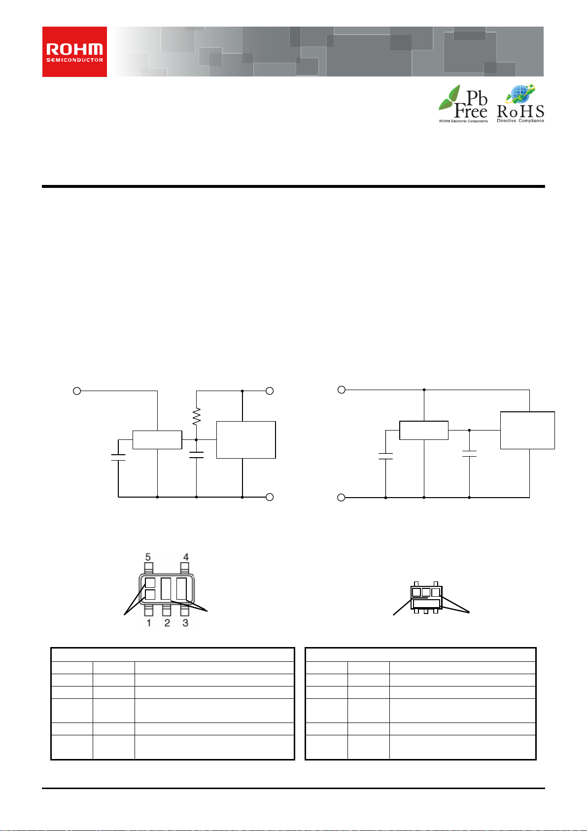
●Ty pical A pplication Circuit
VDD1
●Connection Diagram
SSOP5 VSOF5
TOP VIEW
●Pin Descriptions
PIN No. Symbol Function PIN No. Symbol Function
○Product structure:Silicon monolithic integrated circuit ○This product is not designed protection against radioactive rays.
www.rohm.com © 2011 ROHM Co., Ltd. All rights reserved.
TSZ22111・14・001
CT
Marking
1 VOUT Reset Output 1 VOUT Reset Output
2 VDD Power Supply Voltage 2 SUB Substrate*
3 GND GND 3 CT
4 N.C. Unconnected Terminal 4 GND GND
5 CT
1/10
BD52xx
Open Drain Output type
BD52xx Series
VOUT VDD GND
R
L
Micro
RST
controller
CL
(Capacitor for
noise filtering)
T
N.C. C
Lot. No
SSOP5 VSOF5
Capacitor connection terminal for
output delay time
VDD2
GND
●Key Specifications
Detection voltage: 2.3V to 6.0V (Typ.)
0.1V steps
High accuracy detection voltage: ±1.0%
Ultra-low current consumption: 0.95µA (Typ.)
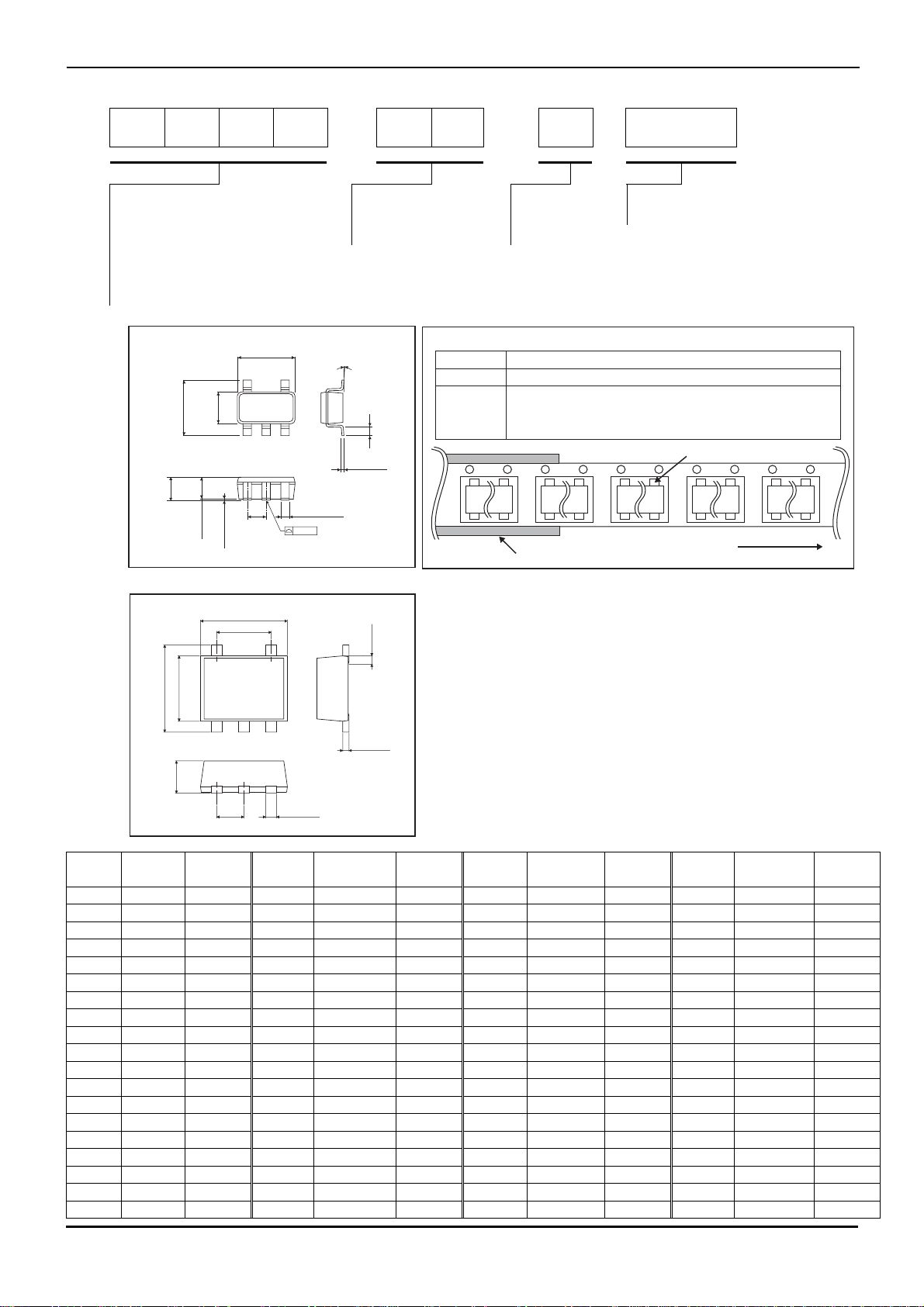
●Package
SSOP5: 2.90mm x 2.80mm x 1.15mm
VSOF5: 1.60mm x 1.60mm x 0.60mm
●Applications
All electronic devices that use micro controllers and logic
circuits
VDD1
CT
GND
CMOS Output type
TOP VIEW
Marking
VOUT SUB CT
Capacitor connection terminal for
5 V
*Connect the substrate to GND.
DD Power Supply Voltage
BD53xx
BD53xx Series
GND
VDD
4
5
2
3
1
output delay time
CL
(Capacitor for
noise filtering)
Lot. No
TSZ02201-0R7R0G300040-1-2
19.DEC.2011 Rev.002
RST
Micro
controller
BD52xx series BD53xx series
Datasheet
●Ordering Information
B D 5 2 2 3 G - T R
BD52: Adjustable Delay Time Reset Voltage Value Package Packaging and forming specification
CMOS Reset IC 23: 2.3V to (0.1V step) G: SSOP5 TR: Embossed tape and reel
Open Drain Type 60: 6.0V FVE: VSOF5
BD53: Adjustable Delay Time
CMOS Reset IC
CMOS Output Type
●Lineup
Marking
PW 6.0V BD5260 PB 4.1V BD5241 RW 6.0V BD5360 RB 4.1V BD5341
PV 5.9V BD5259 PA 4.0V BD5240 RV 5.9V BD5359 RA 4.0V BD5340
PU 5.8V BD5258 MV 3.9V BD5239 RU 5.8V BD5358 QV 3.9V BD5339
PT 5.7V BD5257 MU 3.8V BD5238 RT 5.7V BD5357 QU 3.8V BD5338
PS 5.6V BD5256 MT 3.7V BD5237 RS 5.6V BD5356 QT 3.7V BD5337
PR 5.5V BD5255 MS 3.6V BD5236 RR 5.5V BD5355 QS 3.6V BD5336
PQ 5.4V BD5254 MR 3.5V BD5235 RQ 5.4V BD5354 QR 3.5V BD5335
PP 5.3V BD5253 MQ 3.4V BD5234 RP 5.3V BD5353 QQ 3.4V BD5334
PN 5.2V BD5252 MP 3.3V BD5233 RN 5.2V BD5352 QP 3.3V BD5333
PM 5.1V BD5251 MN 3.2V BD5232 RM 5.1V BD5351 QN 3.2V BD5332
PL 5.0V BD5250 MM 3.1V BD5231 RL 5.0V BD5350 QM 3.1V BD5331
PK 4.9V BD5249 ML 3.0V BD5230 RK 4.9V BD5349 QL 3.0V BD5330
PJ 4.8V BD5248 MK 2.9V BD5229 RJ 4.8V BD5348 QK 2.9V BD5329
PH 4.7V BD5247 MJ 2.8V BD5228 RH 4.7V BD5347 QJ 2.8V BD5328
PG 4.6V BD5246 MH 2.7V BD5227 RG 4.6V BD5346 QH 2.7V BD5327
PF 4.5V BD5245 MG 2.6V BD5226 RF 4.5V BD5345 QG 2.6V BD5326
PE 4.4V BD5244 MF 2.5V BD5225 RE 4.4V BD5344 QF 2.5V BD5325
PD 4.3V BD5243 ME 2.4V BD5224 RD 4.3V BD5343 QE 2.4V BD5324
PC 4.2V BD5242 MD 2.3V BD5223 RC 4.2V BD5342 QD 2.3V BD5323
SSOP5
1.25Max.
VSOF5
1.6± 0.05
0.6MAX
Detection
Voltage
+0.2
−0.1
2.8±0.2
1.6
1.1±0.05
0.05±0.05
1.6± 0.05
1.0± 0.05
5
1.2± 0.05
(MAX 1.28 include BURR)
1
0.5
Part
Number
2.9±0.2
5
12
0.95
2
Marking
4
3
0.22± 0.05
4
3
0.42
0.1
+
6
°
4
−4
0.13
+0.05
−0.04
(Unit : mm)
0.13± 0.05
(Unit : mm)
Detection
Voltage
°
°
+0.05
−0.03
0.2MAX
0.2Min.
<Tape and Reel information>
Embossed carrier tapeTape
Quantity
Direction
of feed
Part
Number
3000pcs
TR
The direction is the 1pin of product is at the upper right when you hold
()
reel on the left hand and you pull out the tape on the right hand
Reel
Marking
Detection
Voltage
1pin
Direction of feed
Order quantity needs to be multiple of the minimum quantity.
∗
Part
Number
Marking
Detection
Voltage
Number
Part
www.rohm.com © 2011 ROHM Co., Ltd. All rights reserved.
TSZ22111・15・001
2/10
TSZ02201-0R7R0G300040-1-2
19.DEC.2011 Rev.002
BD52xx series BD53xx series
z Absolute maximum ratings (Ta=25°C)
Parameter Symbol Limits Unit
Power Supply Voltage VDD-GND -0.3 ~ +10 V
Output Voltage
Dissipation
Nch Open Drain Output GND-0.3 ~ +10
CMOS Output
SSOP5
VSOF5
*1*3
*2*3
V
OUT
540 Power
Pd
GND-0.3 ~ V
210
DD
+0.3
mW
Operating Temperature Topr -40 ~ +105 °C
Ambient Storage Temperature Tstg -55 ~ +125 °C
*1 Use above Ta=25°C results in a 5.4mW loss per degree.
*2 Use above Ta=25°C results in a 2.1mW loss per degree.
*3 When a ROHM standard circuit board (70mm×70mm×1.6mm glass epoxy board) is mounted.
●Electrical characteristics (Unless Otherwise Specified Ta=-40 to 105°C)
Parameter Symbol Condition
Detection Voltage V
VDD=HÆL, RL=470k
DET
Circuit Current when ON IDD1 VDD=VDET-0.2V
Circuit Current when OFF IDD2 VDD=VDET+2.0V
Operating Voltage Range VOPL
‘Low’ Output Current (Nch) IOL
VOL0.4V, Ta=25~105°C, RL=470k 0.95 - -
V
OL0.4V, Ta=-40~25°C, RL=470k 1.20 - -
VDS=0.5V VDD=1.2V 0.4 1.2 -
V
DS=0.5V VDD=2.4V 2.0 5.0 -
Min. Typ. Max.
DET(T)
V
*1
×0.99
V
=2.3-3.1V - 0.80 2.40
DET
V
=3.2-4.2V - 0.85 2.55
DET
V
=4.3-5.2V - 0.90 2.70
DET
=5.3-6.0V - 0.95 2.85
V
DET
V
=2.3-3.1V - 0.75 2.25
DET
V
=3.2-4.2V - 0.80 2.40
DET
V
=4.3-5.2V - 0.85 2.55
DET
V
=5.3-6.0V - 0.90 2.70
DET
Limit
V
DET(T)
VDS=0.5V VDD=4.8V VDET=2.3-4.2V 0.7 1.4 -
‘High’ Output Current (Pch) IOH
VDS=0.5V VDD=6.0V VDET=4.3-5.2V 0.9 1.8 -
VDS=0.5V VDD=8.0V VDET=5.3-6.0V 1.1 2.2 -
Leak Current when OFF I
VDD=VDS=10V
leak
VDD=VDET×1.1, VDET=2.3-2.6V, RL=470k
VDD=VDET×1.1, VDET=2.7-4.2V, RL=470k
CT pin Threshold Voltage VCTH
VDD=VDET×1.1, VDET=4.3-5.2V, RL=470k
V
DD=VDET×1.1, VDET=5.3-6.0V, RL=470k
Output Delay Resistance RCT VDD=VDET×1.1 VCT=0.5V
CT pin Output Current ICT
Detection Voltage
Temperature coefficient
VDET/T Ta=-40°C to 105°C - ±100 ±360 ppm/°C
VCT=0.1V VDD=0.95V
V
CT=0.5V VDD=1.5V 150 240 -
Hysteresis Voltage VDET VDD=LÆHÆL, RL=470k
*1
- - 0.1 µA
DD
V
×0.30
VDD
×0.30
VDD
×0.35
VDD
×0.40
*1
5.5 9 12.5 M
*1
15 40 -
VDET
×0.03
VDD
×0.40
VDD
×0.45
VDD
×0.50
VDD
×0.50
VDET
×0.05
VDET (T) : Standard Detection Voltage (2.3V to 6.0V, 0.1V step)
RL: Pull-up resistor to be connected between VOUT and power supply.
Designed Guarantee. (Outgoing inspection is not done on all products.)
*1 Guarantee is Ta=25°C.
V
Datasheet
DET(T)
V
×1.01
VDD
×0.60
VDD
×0.60
VDD
×0.60
VDD
×0.60
VDET
×0.08
Unit
V
µA
µA
V
mA
mA
V
µA
V
www.rohm.com © 2011 ROHM Co., Ltd. All rights reserved.
TSZ22111・15・001
3/10
TSZ02201-0R7R0G300040-1-2
19.DEC.2011 Rev.002
BD52xx series BD53xx series
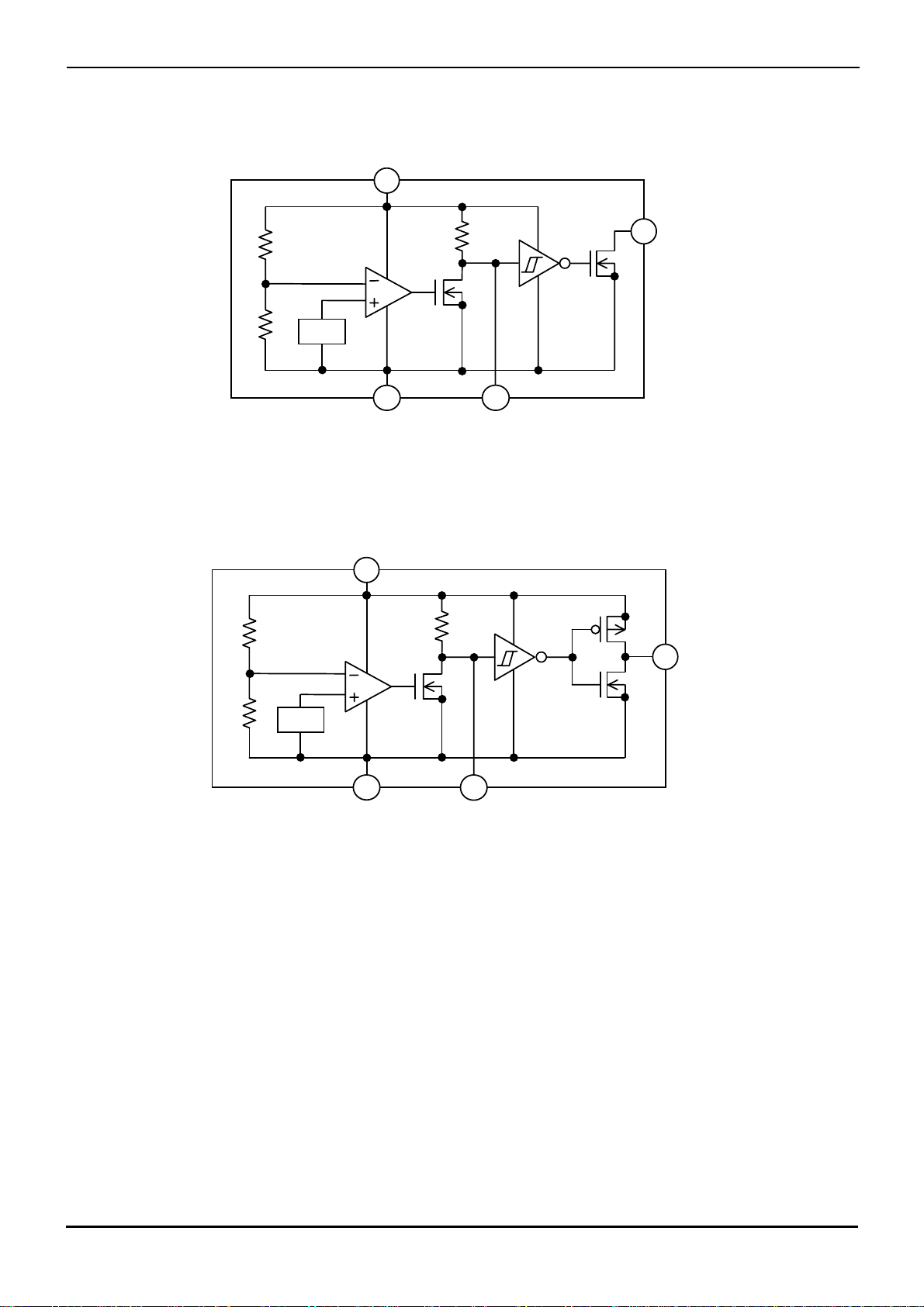
●Block Diagrams
Vref
VDD
Vref
VDD
GND
Fig.1 BD52xx Series
GND
Fig.2 BD53xx Series
Datasheet
OUT
V
CT
OUT
V
CT
www.rohm.com © 2011 ROHM Co., Ltd. All rights reserved.
TSZ22111・15・001
4/10
TSZ02201-0R7R0G300040-1-2
19.DEC.2011 Rev.002

BD52xx series BD53xx series
●Typical Performance Curves
Datasheet
2.0
[A]
DD
1.5
I
:
1.0
0.5
CIRCUIT CURRENT
0.0
0123 456 78 910
V
SUPPLY VOLTAGE :VDD[V]
DD
Fig.3 Circuit Current
BD5242G/FVE
【
【BD5242】
【BD5342】
】
18
BD5242G/F VE
【
[mA]
OL
I
:
15
12
【BD5242】
【BD5342】
VDD=2.4V
9
6
"LOW" OUTPUT CURRENT
3
0
VDD=1.2V
0.0 0.5 1.0 1.5 2.0 2.5
DRAIN-SOURCE VOLTAGE : V
Fig.4 “Low” Output Current
DS
】
[V]
45
BD5342G/F VE
【
[mA]
OH
I
:
40
35
【BD5342】
30
25
20
VDD=8.0V
15
10
5
0
"HIGH" OUTPUT CURRENT
VDD=6.0V
VDD=4.8V
0123456
DR AIN- SOUR C E VOLTAGE : V
Fig.5 “High” Output Current
DS
】
[V]
9
8
[V]
7
OUT
V
:
6
5
4
3
2
OUTPUT VOLTAGE
1
Ta=25
0
00.5 11.522.533.544.555.5
VDD SUPPLY VOLTAGE :VDD[V]
Fig.6 I/O Characteristics
℃
BD5242G/FVE
【
【BD5242】
【BD5342】
Ta=25
℃
】
www.rohm.com © 2011 ROHM Co., Ltd. All rights reserved.
TSZ22111・15・001
5/10
TSZ02201-0R7R0G300040-1-2
19.DEC.2011 Rev.002

BD52xx series BD53xx series
Datasheet
1.0
BD5242G/FVE
【
[V]
OUT
V
:
0.8
【BD5242】
【BD5342】
0.6
0.4
0.2
OUTPUT VOLTAGE
0.0
0.0 0.5 1.0 1.5 2.0 2.5
SUPPLY VOLTAGE : VDD[V]
V
DD
Fig.7 Operating Limit Voltage
】
[A]
CT
I
:
CT OUTPUT CURRENT
450
400
350
【
【BD5242】
【BD5342】
】
BD5242G/F VE
300
250
200
150
100
50
0
012345
V
SUPPLY VOLTAGE : VDD[V]
DD
Fig.8 CT Terminal Current
5.6
BD5242G/F VE
【BD5242】
[V]
5.2
DET
V
:
4.8
Low to hig h(V
【
【BD5342】
DET
4.4
4.0
High to low(V
3.6
~
~
DETECTION VOLTAGE
3.2
-40 0 40 80
TEMPERATURE : Ta[℃]
Fig.9 Detection Voltage
Release Voltage
+ΔV
DET
DET
1.5
】
)
[A]
DD1
I
:
1.0
【BD5242】
BD5242G/FVE
【
【BD5342】
】
0.5
)
0.0
CIRCUIT CURRENT WHEN ON
-40 - 20 0 20 40 60 80 100
TEM PERATURE : Ta[℃]
Fig.10 Circuit Current when ON
www.rohm.com © 2011 ROHM Co., Ltd. All rights reserved.
TSZ22111・15・001
6/10
TSZ02201-0R7R0G300040-1-2
19.DEC.2011 Rev.002

BD52xx series BD53xx series
Datasheet
1.5
【BD5242】
BD5242G/FVE
[A]
DD2
I
:
【
【BD5342】
1.0
0.5
CIRCUIT CURRENT WHEN OFF
0.0
-40 - 20 0 20 40 60 80 100
TEM PERATURE : Ta[℃]
Fig.11 Circuit Current when OFF
】
1.5
BD5242G/FVE
【BD5242】
[V]
OPL
V
:
【
【BD5342】
1.0
0.5
MINIMUM OPERATING VOLTAGE
0.0
-40-20020406080100
TEM PERATU RE : Ta[℃]
Fig.12 Operating Limit Voltage
】
13
【BD5242】
BD5242G/FVE
【
【BD5342】
CT
:
[M]
R
12
11
10
T
9
8
7
6
5
RESISTAN C E OF C
4
-40 - 20 0 20 40 60 80 100
TEMPERATURE : Ta[℃]
Fig.13 CT Terminal Circuit Resistance
】
10000
BD5242G/F VE
【
【BD5242】
1000
[ms]
PLH
100
t
:
10
1
DELAY T IM E
0.1
0.0001 0.001 0.01 0.1
CAPAC IT ANCE OF C
Fig.14 Delay Time (t
C
Terminal External Capacitance
T
【BD5342】
: CCT[F]
T
PLH
】
) and
www.rohm.com © 2011 ROHM Co., Ltd. All rights reserved.
TSZ22111・15・001
7/10
TSZ02201-0R7R0G300040-1-2
19.DEC.2011 Rev.002

BD52xx series BD53xx series
V
Datasheet
●Application Information
Explanation of Operation
For both the open drain type (Fig.15) and the CMOS output type (Fig.16), the detection and release voltages are used as
threshold voltages. When the voltage applied to the V
pins reaches the applicable threshold voltage, the V
DD
OUT
voltage switches from either “High” to “Low” or from “Low” to “High”. Because the BD52xx series uses an open drain output
type, it is possible to connect a pull-up resistor to V
becomes V
V
or the voltage of the other power supply].
DD
DD
R1
Vref
GND
R2
Q3
R3
CT
or another power supply [The output “High” voltage (V
DD
VDD
DD
V
R1
Vref
R2
R3
GND
Q1
RL
RESET
OUT
V
Q3
) in this case
OUT
DD
V
CT
Q2
Q1
Fig.15 (BD52xxType Internal Block Diagram) Fig.16 (BD53xxType Internal Block Diagram)
Setting of Detector Delay Time
This detector IC can be set delay time at the rise of VDD by the capacitor connected to CT terminal.
Delay time at the rise of V
+V
voltage(V
DET
DET
)
t
= -CCT×RCT×ln
PLH
: CT pin Externally Attached Capacitance R
C
CT
V
: CT pin Threshold Voltage(P.2 V CTH refer.) ln : Natural Logarithm
CTH
:Time until when Vout rise to 1/2 of V
DD tPLH
VDD-V
CTH
V
DD
after VDD rise up and beyond the release
DD
: CT pin Internal Impedance (P.2 RCT refer.)
CT
Reference Data of Falling Time (t
Examples of Falling Time (t
Part Number t
) Output
PHL
) Output
PHL
[µs] -40°C t
PHL
[µs] ,+25°C t
PHL
[µs],+105°C
PHL
BD5227 30.8 30 28.8
BD5327 26.8 26 24.8
*This data is for reference only.
The figures will vary with the application, so please confirm actual operating conditions before use.
Timing Waveforms
Example: the following shows the relationship between the input voltage VDD, the CT Terminal Voltage VCT and the output
VOUT when the input power supply voltage VDD is made to sweep up and sweep down (The circuits are those in
voltage
Fig.15 and 16).
1
VDD
VDET+ΔVDET
CT
0V
VDET
VOPL
1/2 VDD
⑤
When the power supply is turned on, the output is unsettled from
after over the operating limit voltage (V
OPL) until tPHL. There fore it is
possible that the reset signal is not outputted when the rise time of
V
is faster than tPHL.
DD
2
When VDD is greater than VOPL but less than the reset release
voltage (V
DET+VDET), the C
terminal (VCT) and output (VOUT)
T
voltages will switch to L.
3
If VDD exceeds the reset release voltage (VDET+VDET), then
V
OUT switches from L to H (with a delay to the C
4
If VDD drops below the detection voltage (VDET) when the power
terminal).
T
supply is powered down or when there is a power supply fluctuation,
V
VOUT
tPHL
tPLH
tPLH
tPHL
OUT switches to L (with a delay of tPHL).
5
The potential difference between the detection voltage and the
release voltage is known as the hysteresis width (V
DET). The
system is designed such that the output does not flip-flop with power
①
② ③ ④
Fig.17 Timing Waveform
supply fluctuations within this hysteresis width, preventing
malfunctions due to noise
terminal
RESET
OUT
V
www.rohm.com © 2011 ROHM Co., Ltd. All rights reserved.
TSZ22111・15・001
8/10
TSZ02201-0R7R0G300040-1-2
19.DEC.2011 Rev.002

BD52xx series BD53xx series
Circuit Applications
●Examples of a common power supply detection reset circuit
VDD1
R
L
Micro
BD52xx
T
C
RST
CL
(Noise-filtering
Capacitor)
controller
Fig.18 Open Drain Output Type
VDD1
BD53xx
RST
CT
CL
(Noise-filtering
Capacitor)
GND
Fig.19 CMOS Output Type
VDD2
GND
Micro
controller
Datasheet
Application examples of BD52xx series (Open Drain
output type) and BD53xx series (CMOS output type) are
shown below.
CASE1: the power supply of the microcontroller (V
differs from the power supply of the reset detection (V
Use the open drain output type (BD52xx) attached a load
resistance (R
) between the output and V
L
. (As shown
DD2
Fig.15)
CASE2: the power supply of the microcontroller (V
same as the power supply of the reset detection (V
Use CMOS output type (BD53xx) or open drain output
type (BD52xx) attached a load resistance (R
the output and V
. (As shown Fig.16)
DD1
) between
L
When a capacitance C
the V
pin (the reset signal input terminal of the
OUT
for noise filtering is connected to
L
microcontroller), please take into account the waveform of
the rise and fall of the output voltage (V
OUT
).
DD1
DD1
DD1
).
DD2
).
) is
)
www.rohm.com © 2011 ROHM Co., Ltd. All rights reserved.
TSZ22111・15・001
9/10
TSZ02201-0R7R0G300040-1-2
19.DEC.2011 Rev.002

BD52xx series BD53xx series
Datasheet
●Operational Notes
1 . Absolute maximum range
Absolute Maximum Ratings are those values beyond which the life of a device may be destroyed. We cannot be defined the
failure mode, such as short mode or open mode. Therefore a physical security countermeasure, like fuse, is to be given
when a specific mode to be beyond absolute maximum ratings is considered.
2 . GND potential
GND terminal should be a lowest voltage potential every state.
Please make sure all pins, which are over ground even if, include transient feature.
3 . Electrical Characteristics
Be sure to check the electrical characteristics that are one the tentative specification will be changed by temperature,
supply voltage, and external circuit.
4 . Bypass Capacitor for Noise Rejection
Please put into the capacitor of 1µF or more between V
pin and GND, and the capacitor of about 1000pF between V
DD
OUT
and GND, to reject noise. If extremely big capacitor is used, transient response might be late. Please confirm sufficiently for
the point.
5 . Short Circuit between Terminal and Soldering
Don’t short-circuit between Output pin and V
pin, Output pin and GND pin, or VDD pin and GND pin. When soldering the
DD
IC on circuit board, please be unusually cautious about the orientation and the position of the IC. When the orientation is
mistaken the IC may be destroyed.
6 . Electromagnetic Field
Mal-function may happen when the device is used in the strong electromagnetic field.
7 . The V
8. A V
9 . Lower than the mininum input voltage makes the V
line inpedance might cause oscillation because of the detection current.
DD
-GND capacitor (as close connection as possible) should be used in high VDD line impedance condition.
DD
OUT high impedance, and it must be VDD in pull up (VDD) condition.
10. This IC has extremely high impedance terminals. Small leak current due to the uncleanness of PCB surface might cause
unexpected operations. Application values in these conditions should be selected carefully. If the leakage is assumed
between the V
resistance. If 10M leakage is assumed between the C
terminal and the V
connected to C
terminal and the GND terminal, the pull-up resistor should be less than 1/10 of the assumed leak
OUT
terminal and the GND terminal, 1M connection between the CT
T
DD terminal would be recommended. The value of RCT depends on the external resistor that is
terminal, so please consider the delay time that is decided by ×RCT×C
T
changes.
CT
11. External parameters
The recommended parameter range for C
T is 100pF~0.1µF and RL is 50k~1M. There are many factors (board layout,
etc) that can affect characteristics. Please verify and confirm using practical applications.
12. Power on reset operation
Please note that the power on reset output varies with the V
rise up time. Please verify the actual operation.
DD
13. Precautions for board inspection
Connecting low-impedance capacitors to run inspections with the board may produce stress on the IC. Therefore, be
certain to use proper discharge procedure before each process of the test operation.
To prevent electrostatic accumulation and discharge in the assembly process, thoroughly ground yourself and any
equipment that could sustain ESD damage, and continue observing ESD-prevention procedures in all handing, transfer
and storage operations. Before attempting to connect components to the test setup, make certain that the power supply is
OFF. Likewise, be sure the power supply is OFF before removing any component connected to the test setup.
14. When the power supply, is turned on because of in certain cases, momentary Rash-current flow into the IC at the logic
unsettled, the couple capacitance, GND pattern of width and leading line must be considered.
pin
Status of this document
The Japanese version of this document is formal specification. A customer may use this translation version only for a reference
to help reading the formal version.
If there are any differences in translation version of this document formal version takes priority.
www.rohm.com © 2011 ROHM Co., Ltd. All rights reserved.
TSZ22111・15・001
10/10
TSZ02201-0R7R0G300040-1-2
19.DEC.2011 Rev.002

Datasheet
Datasheet
Notice
●Precaution for circuit design
1) The products are designed and produced for application in ordinary electronic equipment (AV equipment, OA
equipment, telecommunication equipment, home appliances, amusement equipment, etc.). If the products are to be
used in devices requiring extremely high reliability (medical equipment, transport equipment, aircraft/spacecraft,
nuclear power controllers, fuel controllers, car equipment including car accessories, safety devices, etc.) and whose
malfunction or operational error may endanger human life and sufficient fail-safe measures, please consult with the
ROHM sales staff in advance. If product malfunctions may result in serious damage, including that to human life,
sufficient fail-safe measures must be taken, including the following:
[a] Installation of protection circuits or other protective devices to improve system safety
[b] Installation of redundant circuits in the case of single-circuit failure
2) The products are designed for use in a standard environment and not in any special environments. Application of the
products in a special environment can deteriorate product performance. Accordingly, verification and confirmation of
product performance, prior to use, is recommended if used under the following conditions:
[a] Use in various types of liquid, including water, oils, chemicals, and organic solvents
[b] Use outdoors where the products are exposed to direct sunlight, or in dusty places
[c] Use in places where the products are exposed to sea winds or corrosive gases, including Cl
and NO
[d] Use in places where the products are exposed to static electricity or electromagnetic waves
[e] Use in proximity to heat-producing components, plastic cords, or other flammable items
[f] Use involving sealing or coating the products with resin or other coating materials
[g] Use involving unclean solder or use of water or water-soluble cleaning agents for cleaning after soldering
[h] Use of the products in places subject to dew condensation
2
2, H2S, NH3, SO2,
3) The products are not radiation resistant.
4) Verification and confirmation of performance characteristics of products, after on-board mounting, is advised.
5) In particular, if a transient load (a large amount of load applied in a short period of time, such as pulse) is applied,
confirmation of performance characteristics after on-board mounting is strongly recommended. Avoid applying power
exceeding normal rated power; exceeding the power rating under steady-state loading condition may negatively affect
product performance and reliability.
6) De-rate Power Dissipation (Pd) depending on Ambient temperature (Ta).
When used in sealed area, confirm the actual ambient temperature.
7) Confirm that operation temperature is within the specified range described in product specification.
8) Failure induced under deviant condition from what defined in the product specification cannot be guaranteed.
●Precaution for Mounting / Circuit board design
1) When a highly active halogenous (chlorine, bromine, etc.) flux is used, the remainder of flux may negatively affect
product performance and reliability.
2) In principle, the reflow soldering method must be used; if flow soldering method is preferred, please consult with the
Company in advance.
Regarding Precaution for Mounting / Circuit board design, please specially refer to ROHM Mounting specification
●Precautions Regarding Application Examples and External Circuits
1) If change is made to the constant of an external circuit, allow a sufficient margin due to variations of the characteristics
of the products and external components, including transient characteristics, as well as static characteristics.
2) The application examples, their constants, and other types of information contained herein are applicable only when
the products are used in accordance with standard methods. Therefore, if mass production is intended, sufficient
consideration to external conditions must be made.
Notice - Rev.001

Datasheet
●Precaution for Electrostatic
This product is Electrostatic sensitive product, which may be damaged due to Electrostatic discharge. Please take proper
caution during manufacturing and storing so that voltage exceeding Product maximum rating won't be applied to products.
Please take special care under dry condition (e.g. Grounding of human body / equipment / solder iron, isolation from
charged objects, setting of Ionizer, friction prevention and temperature / humidity control).
●Precaution for Storage / Transportation
1) Product performance and soldered connections may deteriorate if the products are stored in the following places:
[a] Where the products are exposed to sea winds or corrosive gases, including Cl2, H2S, NH3, SO2, and NO2
[b] Where the temperature or humidity exceeds those recommended by the Company
[c] Storage in direct sunshine or condensation
[d] Storage in high Electrostatic
2) Even under ROHM recommended storage condition, solderability of products out of recommended storage time period
may be degraded. It is strongly recommended to confirm solderability before using products of which storage time is
exceeding recommended storage time period .
3) Store / transport cartons in the correct direction, which is indicated on a carton as a symbol. Otherwise bent leads may
occur due to excessive stress applied when dropping of a carton.
4) Use products within the specified time after opening a dry bag.
●Precaution for product label
QR code printed on ROHM product label is only for internal use, and please do not use at customer site. It might contain a
internal part number that is inconsistent with an product part number.
●Precaution for disposition
When disposing products please dispose them properly with a industry waste company.
●Precaution for Foreign exchange and Foreign trade act
Since concerned goods might be fallen under controlled goods prescribed by Foreign exchange and Foreign trade act,
please consult with ROHM in case of export.
●Prohibitions Regarding Industrial Property
1) Information and data on products, including application examples, contained in these specifications are simply for
reference; the Company does not guarantee any industrial property rights, intellectual property rights, or any other
rights of a third party regarding this information or data. Accordingly, the Company does not bear any responsibility for:
[a] infringement of the intellectual property rights of a third party
[b] any problems incurred by the use of the products listed herein.
2) The Company prohibits the purchaser of its products to exercise or use the intellectual property rights, industrial
property rights, or any other rights that either belong to or are controlled by the Company, other than the right to use,
sell, or dispose of the products.
Datasheet
Notice - Rev.001
 Loading...