

Datasheet
4-Channel Charge Pump
White LED Driver with 64
Dimming Steps and 1-wire Serial Interface
BD1601MUV
●General Description
The multi-level brightness control white LED driver not
only ensures efficient boost by automatically changing
the boost rate but also works as a constant current
driver in 64 steps, so that the driving current can be
adjusted finely. This IC is best suited to turn on white
LEDs that require high-accuracy LED brightness
control.
●Features
Built-in parallel LED driver for 4 lamps.
64-step LED current adjusts function.
Inter-LED relative current accuracy: 3% or less
Lighting/dimming control via a single-line digital
control interface.
Automatic transition charge pump type DC/DC
converter (×1,×1.5 and ×2).
High efficiency achieved (90% or more at
maximum).
Various protection functions such as output voltage
protection, over current limiter and thermal shutdown
circuit are mounted.
●Key Specifications
Operating power supply voltage range: 2.7V to 5.5V
LED maximum current: 30mA (Typ.)
Oscillator frequency: 1.0MHz(Typ.)
Quiescent Current: 0.1μA (Typ.)
Operating temperature range: -30℃ to +85℃
●Package W(Typ.) x D(Typ.) x H(Max.)
●Applications
This driver is applicable for various fields such as
mobile phones, portable game machines and white
goods.
VQFN016V3030
3.00mm x 3.00mm x 1.00mm
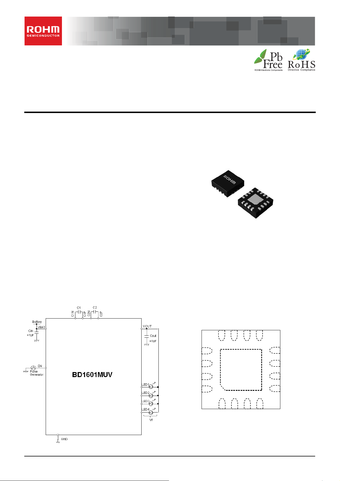
●Typical Application Circuit
White LED Application (Recommended)
●Pin Configuration [Top View]
C2P
GND
12
C2N
C1N
11
9
10
LED1
13
LED2
14
LED3
LED4
15
16
1
2
3
4
NC
EN
GND
NC
○Product structure:Silicon monolithic integrated circuit ○This product is not designed protection against radioactive rays
www.rohm.com
© 2012 ROHM Co., Ltd. All rights reserved.
TSZ22111・14・001
1/14
TSZ02201-0G3G0C200030-1-2
05.Nov.2012 Rev.001
8
7
6
5
C1P
VBAT
VOUT
NC
BD1601MUV
●Absolute Maximum Ratings (Ta=25℃)
Parameter Symbol Ratings Unit
Power supply voltage VMAX 7 V
Operating temperature range Topr -30 to +85 ℃
Storage temperature range Tstg -55 to +150 ℃
Datasheet
Power dissipation Pd 700
(*1) When a glass epoxy substrate (70mm × 70mm × 1.6mm) has been mounted,
this loss will decrease 5.6mW/℃ if Ta is higher than or equal to 25℃.
(*1)
mW
●Recommended Operating Ratings (Ta = -30 to 85℃)
Parameter Symbol Ratings Unit
Operating power supply voltage
Vin 2.7 to 5.5 V
●Electrical Characteristics Unless otherwise noted, Ta = +25℃, VBAT=3.6V
Parameter Symbol
Min. Typ. Max.
Limits
Units Condition
Overall
Quiescent Current Iq - 0.1 1 μA EN=0V
Current Consumption1 I dd1 - 1.0 2.4 mA x1.0 Mode, Except LED current
Current Consumption2 I dd2 - 2.5 3.5 mA x2.0 Mode, Except LED current
Charge Pump
Oscillator frequency fOSC 0.8 1.0 1.2 MHz
Current Source
LED maximum current ILED-max 28.5 30 31.5 mA
LED current accuracy ILED-diff - - 5.0 %
LED current matching
(*1)
ILED-match - 0.5 3.0 %
LED control voltage VLED - 0.2 0.25 V
When LED current 15.5mA setting
and LED terminal voltage 1.0V
When LED current 15.5mA setting
and LED terminal voltage 1.0V
minimum voltage
at LED1 to LED4 pins
Logic control terminal
Low threshold voltage VIL - - 0.4 V
High threshold voltage VIH 1.4 - - V
High level Input current IIH - 0.1 2 μA EN=VBAT
Low level Input current IIL -2 -0.1 - μA EN=0V
Minimum EN High time THI 50 - - ns
Minimum EN Low time TLO 0.05 - 100 μs
EN Off Timeout TOFF - 512 640 μs
(*1) The following expression is used for calculation:
ILED-match={(Imax-Imin)/(Imax+Imin)} × 100
Imax= Current value in a channel with the maximum current value among all channels
Imin=Current value in a channel with the minimum current value among all channels
www.rohm.com
© 2012 ROHM Co., Ltd. All rights reserved.
TSZ22111・15・001
2/14
TSZ02201-0G3G0C200030-1-2
05.Nov.2012 Rev.001
BD1601MUV
●Pin Descriptions
Datasheet
Pin No. Pin name In/Out Type
1 NC - - No connect
2 NC - - No connect
3 EN In C ON/OFF and dimming control
4 GND - D GND
5 NC - - No connect
6 VOUT Out A Charge pump output
7 VBAT - A Power supply
8 C1P In/Out A Flying capacitor pin positive (+) side
9 C1N In/Out B Flying capacitor pin negative (-) side
10 C2N In/Out B Fl ying capacitor pin negative ( -) side
11 C2P In/Out A Flying capacitor pin positive (+) side
12 GND - D GND
13 LED1 Out B LED current driver output 1
14 LED2 Out B LED current driver output 2
15 LED3 Out B LED current driver output 3
16 LED4 Out B LED current driver output 4
-
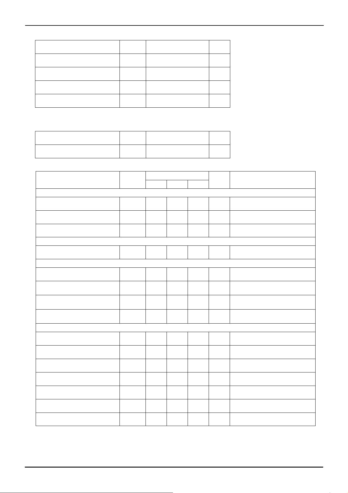
●Pin ESD Type
Type-A
Thermal
PAD
- D
Type-B
Heat radiation PAD of back side
Connect to GND
VBAT Type-C
Function
VBAT
PAD
GND
Type-D
PAD
VBAT
PAD
GND
Figure 1. Pin ESD Type
PAD
GND
www.rohm.com
© 2012 ROHM Co., Ltd. All rights reserved.
TSZ22111・15・001
3/14
TSZ02201-0G3G0C200030-1-2
05.Nov.2012 Rev.001
BD1601MUV
VBAT
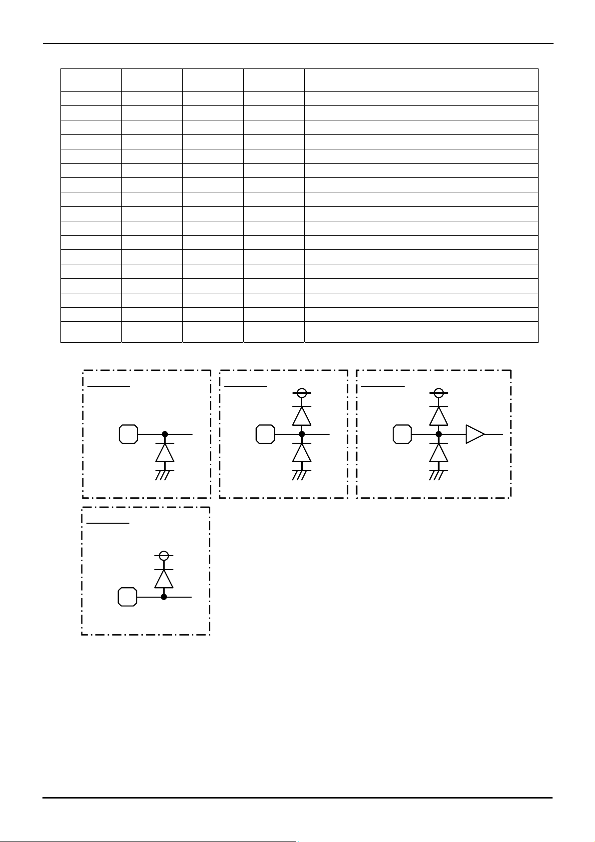
●Block Diagram
Datasheet
C1N C1P C2N C2P
VOUT
Charge Pump
Mode Control
×1, ×1.5, ×2
Charge pump
Over Voltage
Protect
OSC
EN
Enable/
Brightness
Control
6
TSD
Current
DAC
Vout Control
LED1
LED2
LED3
LED4
GND
www.rohm.com
© 2012 ROHM Co., Ltd. All rights reserved.
TSZ22111・15・001
4/14
TSZ02201-0G3G0C200030-1-2
05.Nov.2012 Rev.001
BD1601MUV
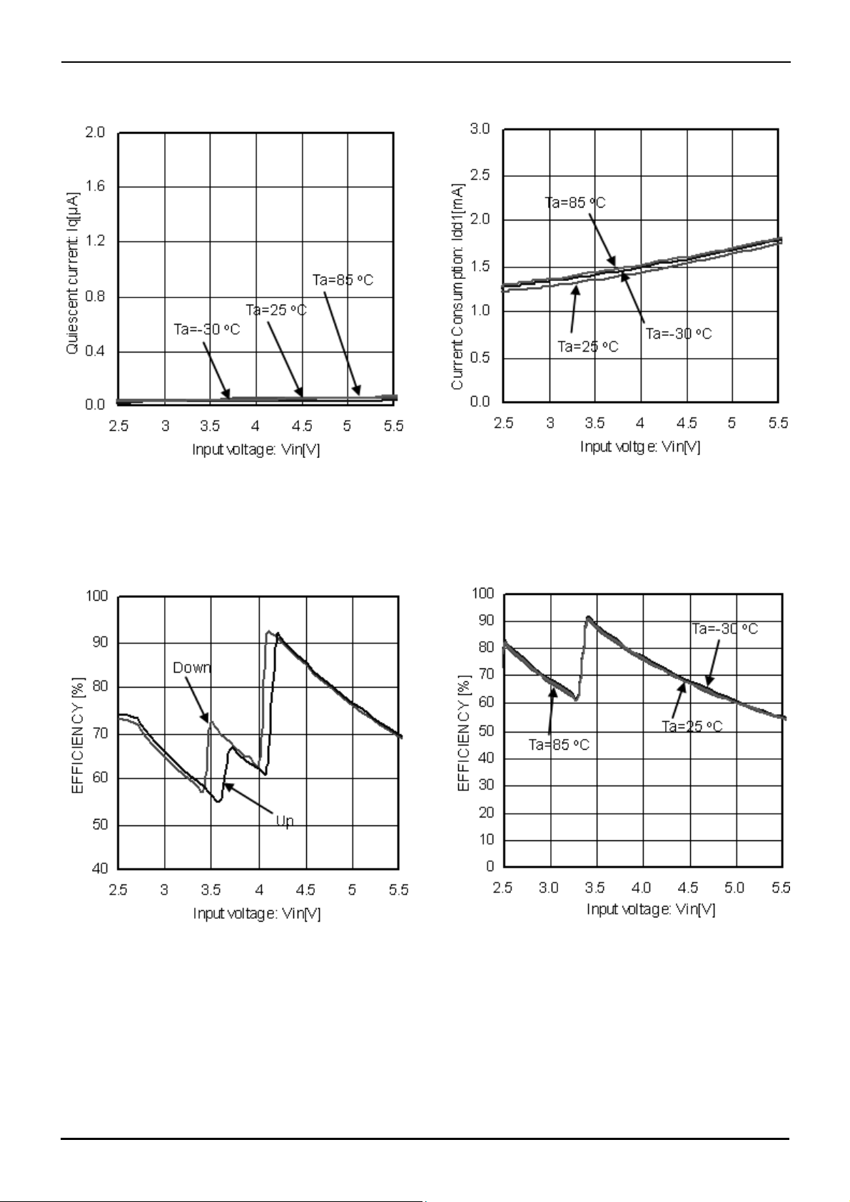
●Typical Performance Curves
Figure 2. Circuit Current
(Standby)
Figure 4. Efficiency
(20mA × 4Lights)
Datasheet
Figure 3. Circuit Current
(Operation in × 1.0Mode)
Figure 5. Efficiency
(5mA × 4Lights)
www.rohm.com
© 2012 ROHM Co., Ltd. All rights reserved.
TSZ22111・15・001
5/14
TSZ02201-0G3G0C200030-1-2
05.Nov.2012 Rev.001
BD1601MUV
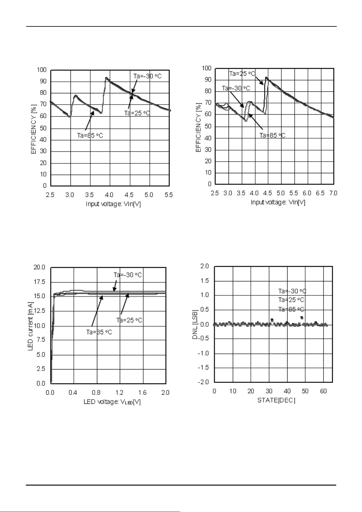
●Typical Performance Curves - continued
Figure 8. LED Current Characteristics
Figure 6. Efficiency
(15mA × 4 Lights)
(LED current 15.5mA)
Datasheet
Figure 7. Efficiency
(30mA × 4Lights)
Figure 9. LED Current Characteristics
(Differential Linearity error)
www.rohm.com
© 2012 ROHM Co., Ltd. All rights reserved.
TSZ22111・15・001
6/14
TSZ02201-0G3G0C200030-1-2
05.Nov.2012 Rev.001

BD1601MUV
●Typical Performance Curves - continued
Figure 10. LED Current Characteristics
(Integral Linearity Error)
Figure 12. LED Current – Input voltage
(LED current 15.5mA)
Datasheet
Figure 11. LED current matching
www.rohm.com
© 2012 ROHM Co., Ltd. All rights reserved.
TSZ22111・15・001
7/14
TSZ02201-0G3G0C200030-1-2
05.Nov.2012 Rev.001

BD1601MUV
●Function Description
(1) LED driver
▪ UPIC interface
BD1601MUV is a single line digital interface control (Uni-port Interface Control=UPIC) that can control the power
ON/OFF and LED current value through the EN pin only. The LED current increments by about 0.5mA depending on
the number of leading edges. When the number of leading edge is added at the maximu m output current of 30mA (64
leading edges), the current is almost equal to 0.5mA at startup time. To maintain any output current, the EN pin must
be kept at “H” level. To power off, the EN pin must be kept at “L” level for more than 640µsec.
EN
Datasheet
T
HI
T
LO
T
OFF
(Internal)
State
I
LED
C1 C2 C3 C4
Soft Start
1.4mA 1.4mA
C3
1.9mA
C5
2.3mA
C63 C64
29.5mA
30mA
C1 C2
0.9mA
0.5mA
OFFOFF
Figure 13. Brightness Control Method
T
HI
T
LO
T
OFF
EN
Figure 14. UPIC Interface
▪ LED current level
The LED current state can be changed by the EN control signal. When the current level is Cn, the basic LED current
(ILED) can be obtained from the following expression (where, n indicates a state number).
I
= 30 / 64 ×n [mA]
LED
State Output current
[mA]
State Output current
[mA]
State Output current
[mA]
State Output current
C1 0.5 C14 8.0 C33 15.5 C49 23.0
C2 0.9 C18 8.4 C34 15.9 C50 23.4
C3 1.4 C19 8.9 C35 16.4 C51 23.9
C4 1.9 C20 9.4 C36 16.9 C52 24.4
C5 2.3 C21 9.8 C37 17.3 C53 24.8
C6 2.8 C22 10.3 C38 17.8 C54 25.3
C7 3.3 C23 10.8 C39 18.3 C55 25.8
C8 3.8 C24 11.3 C40 18.8 C56 26.3
C9 4.2 C25 11.7 C41 19.2 C57 26.7
C10 4.7 C26 12.2 C42 19.7 C58 27.2
C11 5.2 C27 12.7 C43 20.2 C59 27.7
C12 5.6 C28 13.1 C44 20.6 C60 28.1
C13 6.1 C29 13.6 C45 21.1 C61 28.6
C14 6.6 C30 14.1 C46 21.6 C62 29.1
C15 7.0 C31 14.5 C47 22.0 C63 29.5
C16 7.5 C32 15.0 C48 22.5 C64 30.0
[mA]
www.rohm.com
© 2012 ROHM Co., Ltd. All rights reserved.
TSZ22111・15・001
8/14
TSZ02201-0G3G0C200030-1-2
05.Nov.2012 Rev.001

BD1601MUV
(2) Charge pump
a) Description of operations
Pin voltage comparison takes place at VOUT control section, and then VOUT generation takes place so that the LED
cathode voltage with the highest Vf is set to 0.2V. A boost rate is changed automatically to a proper one at the Charge
Pump Mode Control section so that operation can take place at possible low boost rate. When the current taken from
VBAT exceeds 600mA, the overcurrent limiter is activated and this IC is reset. In addition, if the output voltage falls
below 1.5V, this IC is reset for short-circuit at output.
b) Soft start function
BD1601MUV have a soft start function that prevents the rush current.
EN/LED*
VOUT
I
LED
Datasheet
T
OFF
Soft Start Ordinal mode
Figure 15. Soft Start
c) Automatic boost rate change
The boost rate automatically switches to the best mode.
* (×1 mode -> ×1.5 mode) or (×1.5 mode -> ×2 mode)
If a battery voltage drop occursBD1601MUV cannot maintain the LED constant current, and then mode transition begins.
* (×1.5 mode -> ×1 mode) or (×2 mode -> ×1.5 mode)
If a battery voltage rise occurs, VOUT and VBAT detection are activated, and then mode transition begins.
(3) UVLO (Ultra low Voltage Lock Out)
If the input voltage falls below 2.2V, BD1601MUV is shut down to prevent malfunction due to ultra-low voltage.
(4) OVP (Over Voltage Protection)
This circuit protects this IC agai nst damage wh en the C /P outpu t vo lt ag e (VOUT) ri se s extremely fo r some ex terna l facto rs.
(5) Thermal shutdown (TSD)
To protect this IC against thermal damage or heat-driven uncontrolled operations, this circuit turns off the output if the
chip temperature rises over 175℃. In addition, it turns on the output if the temperature returns to the normal temperature.
(6) Power sequence
VBAT
www.rohm.com
© 2012 ROHM Co., Ltd. All rights reserved.
TSZ22111・15・001
EN
Figure 16. Power sequence
9/14
*VBAT voltage ≧ EN voltage
TSZ02201-0G3G0C200030-1-2
05.Nov.2012 Rev.001

BD1601MUV
●Application Circuit Example
White LED Application(VOUT not used)
Battery
C1N
Datasheet
C2N
C1P
C2P
Cin
=1μF
Pulse
Generator
VBAT
EN
Charge Pump
Mode Control
Enable/
Brightness
Control
6
×1, ×1.5, ×2
Charge pump
Over Voltage
Protect
OSC
TSD
Current
DAC
VOUT
Cout
=1μF
VDD
Vout Control
LED1
LED2
LED3
LED4
Vf
GND
Figure 17. Block Diagram and Circuit Example
●Selection of Components Externally Connected
Capacitor (Use a ceramics capacitor with good frequency and temperature characteristics.)
Symbol Recommended value Recommended parts Type
Cout,Cin,C1,C2 1μF GRM188B11A105KA61B(MURATA) Ceramics capacitor
Connect an input bypass capacitor Cin between VBAT and GND pin and an output capacitor Cout between VOUT and GND
pin in proximity. Place both C1P-C1N and C2P-C2N capacitors in proximity to the chip. Furthermore, select a ceramics
capacitor with a sufficient rating for voltage to be applied.
When the parts not listed above are used, the equivalent parts must be used.
www.rohm.com
© 2012 ROHM Co., Ltd. All rights reserved.
TSZ22111・15・001
10/14
TSZ02201-0G3G0C200030-1-2
05.Nov.2012 Rev.001

BD1601MUV
Datasheet
●Recommended PCB Layout
In PCB design, wire the power suppl y line in a way th at the PCB im pedance goes low and provide a bypass capacitor if
needed. Heat radiation of back side PAD is used for improving the efficiency of IC heat radiation. Solder PAD to GND pin.
Moreover, connect ground plane of board using via as shown in the patterns of below page.
The efficiency of heat radiation improves according to the area of ground plane.
To substrat e
GND
GND
C2
Cout
GND
C2
EN
GND
Cin
To substrat e
VCC
Figure 18. Application Layout Image (Top View) Figure 19. BD1601MUV Front (Top View)
Cout
VOUT
VBAT
C1
VOUT
C1
CIN
VBAT
www.rohm.com
© 2012 ROHM Co., Ltd. All rights reserved.
TSZ22111・15・001
11/14
TSZ02201-0G3G0C200030-1-2
05.Nov.2012 Rev.001

BD1601MUV
●Operational Notes
(1) Absolute Maximum Ratings
An excess in the absolute maximum ratings, such as supply voltage, temperatur e range of operating conditions, etc.,
can break down devices, thus making impossible to identify breakin g mode such as a short circuit or an open circuit. If
any special mode exceeding the absolute maximum rat ings is assumed, consid eration should be giv en to take physical
safety measures including the use of fuses, etc.
(2) Operating conditions
These conditions represent a range within which characteristics can be provided approximately as expected. The
electrical characteristics are guaranteed under the conditions of each parameter.
(3) Reverse connection of power supply connector
The reverse connection of power supply connector can break down ICs. Take protective measures against the breakdown due
to the reverse connection, such as mounting an external diode between the power supply and the IC’s pow er supply terminal.
(4) Power supply line
Design PCB pattern to provide low impedance for the wiring between the power supply and the GND lines. Furthermore,
for all power supply terminals to ICs, mount a capacitor between the power supply and t he GND terminal. At the same
time, in order to use an electrolytic capacitor, thoroughly check to be sure the characteristics of the capacitor to be used
present no problem including the occurrence of capacity dropout at a low temperature, thus determining the constant.
(5) GND voltage
Make setting of the potential of the GND terminal so that it will be maintained at the minimum in any operating state.
Furthermore, check to be sure no terminals are at a potential lower than the GND volt age including an actual electric transient.
(6) Short circuit between terminals and erroneous mounting
In order to mount ICs on a set PCB, pay thorough attention to the direction and offset of the ICs. Erroneous mounti ng
can break down the ICs. Furthermore, if a short circuit occurs due to f oreign matters entering between terminals or
between the terminal and the power supply or the GND terminal, the ICs can break down.
(7) Operation in strong electromagnetic field
Be noted that using ICs in the strong electromagnetic field can malfunction them.
(8) Inspection with set PCB
On the inspection with the set PCB, if a capacitor is connected t o a low-im pedance IC ter minal, th e IC can suffer stress.
Therefore, be sure to discharge from the set PCB b y each process. Furthermore, in order to mount or dismount the set
PCB to/from the jig for the inspection process, be sure to turn OFF the power supply and then mount the set PCB to the
jig. After the completion of the inspection, be sure to turn OFF the power supply and then dism ount it from the jig. In
addition, for protection against static electricit y, establish a ground for the assembly process and pay thorough attention
to the transportation and the storage of the set PCB.
(9) Input terminals
In terms of the construction of IC, parasitic elements are inevitably formed i n relation to potential. The operation of the
parasitic element can cause interference with circuit operation, t hus resulting in a malfunction and then breakdown of
the input terminal. Therefore, pay thorough attention not to hand le the input terminals, such as to apply to the input
terminals a voltage lower than the GND respectively, so that any parasitic element will operate. Furthermore, do not
apply a voltage to the input terminals when no power supply voltage is applied to t he IC. In addition, even if the power
supply voltage is applied, apply to the input terminals a voltage lower than the power supply voltage or within the
guaranteed value of electrical characteristics.
(10) Ground wiring pattern
If small-signal GND and large-current GND are provided, It will be recommended to separate the large-current GND
pattern from the small-signal GND pattern and establish a single ground at the reference point of the set PCB so that
resistance to the wiring pattern and voltage fluctuations due to a large c urrent will cause no fluctuations in voltages of
the small-signal GND. Pay attention not to cause fluctuatio ns in the GND wiring pattern of external parts as well.
(11) External capacitor
In order to use a ceramic capacitor as the external capacitor, determine the constant with consideration given to a
degradation in the nominal capacitance due to DC bias and changes in the capacitance due to t emperature, etc.
(12) Thermal shutdown circuit (TSD)
When junction temperatures become 175
OFF. The thermal shutdo wn circuit, which is aimed at isolating the LSI from thermal runa way as much as possible, is
not aimed at the protection or guarantee of the LSI. Therefore, do not cont inuously use the LSI with this circuit operati ng
or use the LSI assuming its operation.
(13) Thermal design
Perform thermal design in which there are adequate margins by taking into account the permissible dissipation (Pd) in
actual states of use.
℃ (typ) or higher, the thermal shutdown circuit operates and turns a switch
Datasheet
Status of this document
The Japanese version of this document is formal specificati on. A customer may use this translation version onl y for a reference
to help reading the formal version.
If there are any differences in translation version of this document formal version takes priority.
www.rohm.com
© 2012 ROHM Co., Ltd. All rights reserved.
TSZ22111・15・001
12/14
TSZ02201-0G3G0C200030-1-2
05.Nov.2012 Rev.001

BD1601MUV
)
●Ordering Information
B D 1 6 0 1 M U V - E 2
Datasheet
Part Number Package
MUV: VQFN016V3030
Packaging and forming specification
E2: Embossed tape and reel
●Marking Diagram
VQFN016V3030 (TOP VIEW
Part Number Marking
BD1
601
LOT Number
1PIN MARK
●Physical Dimension Tape and Reel Information
VQFN016V3030
3.0±0.1
0.4±0.1
1.0MAX
0.08 S
0.75
C0.2
16
13
1.4±0.1
1
12 9
1PIN MARK
0.5
4
5
8
0.25
3.0±0.1
+0.03
+0.05
−0.04
0.02
−0.02
1.4±0.1
S
(0.22)
(Unit : mm)
<Tape and Reel information>
Embossed carrier tapeTape
Quantity
Direction
of feed
3000pcs
E2
The direction is the 1pin of product is at the upper left when you hold
()
reel on the left hand and you pull out the tape on the right hand
Reel
1pin
Order quantity needs to be multiple of the minimum quantity.
∗
Direction of feed
www.rohm.com
© 2012 ROHM Co., Ltd. All rights reserved.
TSZ22111・15・001
13/14
TSZ02201-0G3G0C200030-1-2
05.Nov.2012 Rev.001

BD1601MUV
●Revision History
Date Revision Changes
05.Nov.2012 001 New Release
Datasheet
www.rohm.com
© 2012 ROHM Co., Ltd. All rights reserved.
TSZ22111・15・001
14/14
TSZ02201-0G3G0C200030-1-2
05.Nov.2012 Rev.001

Datasheet
Datasheet
Notice
●General Precaution
1) Before you use our Products, you are requested to carefully read this document and fully understand its contents.
ROHM shall not be in any way responsible or liable for failure, malfunction or accident arising from the use of a ny
ROHM’s Products against warning, caution or note contained in this document.
2) All information contained in this document is current as of the issuing date and subject to change without any prior
notice. Before purchasing or using ROHM’s Products, please confirm the latest information with a ROHM sales
representative.
●Precaution on using ROHM Products
1) Our Products are designed and manufactured for application in ordinary electronic equipments (such as AV equipment ,
OA equipment, telecommunication equipment, home electronic appliances, amusement equipment, etc.). If you
intend to use our Products in devices requiring extremely high reliability (such as medical equipment, transport
equipment, traffic equipment, aircraft/spacecraft, nuclear power controllers, fuel controllers, car equipment including car
accessories, safety devices, etc.) and whose malfunction or failure may cause loss of human life, bodily injury or
serious damage to property (“Specific Applications”), please consult with the ROHM sales representative in advance.
Unless otherwise agreed in writing by ROHM in advance, ROHM shall not be in any way respons ible or liable for any
damages, expenses or losses incurred by you or third parties arising from the use of any ROHM’s Products for Specific
Applications.
2) ROHM designs and manufactures its Products subject to strict quality control system. However, semiconductor
products can fail or malfunction at a certain rate. Please be sure to implement, at your own responsibilities, adequate
safety measures including but not limited to fail-safe design against the physical injury, damage to any propert y, which
a failure or malfunction of our Products may cause. The following are examples of safety measures:
[a] Installation of protection circuits or other protective devices to improve system safety
[b] Installation of redundant circuits to reduce the impact of single or multiple circuit failure
3) Our Products are designed and manufactured for use under standard conditions and not under any special or
extraordinary environments or conditions, as exemplified below. Accordingly, ROHM shall not be in any way
responsible or liable for any damages, expenses or losses arising from the use of any ROHM’s Products under any
special or extraordinary environments or conditions. If you intend to use our Products under any special or
extraordinary environments or conditions (as exemplified below), your independent verification and confirmation of
product performance, reliability, etc, prior to use, must be necessary:
[a] Use of our Products in any types of liquid, including water, oils, chemicals, and organic solvents
[b] Use of our Products outdoors or in places where the Products are exposed to direct sunlight or dust
[c] Use of our Products in places where the Products are exposed to sea wind or corrosive gases, including Cl
2S, NH3, SO2, and NO2
H
[d] Use of our Products in places where the Products are exposed to static electricity or electromagnetic waves
[e] Use of our Products in proximity to heat-producing components, plastic cords, or other flammable items
[f] Sealing or coating our Products with resin or other coating materials
[g] Use of our Products without cleaning residue of flux (even if you use no-clean type fluxes, cleaning residue of
flux is recommended); or Washing our Products by using water or water-solub le cleaning agents for cleaning
residue after soldering
[h] Use of the Products in places subject to dew condensation
4) The Products are not subject to radiation-proof design.
5) Please verify and confirm characteristics of the final or mounted products in using the Products.
6) In particular, if a transient load (a large amount of load applied in a short per iod of time, such as pulse) is applied,
confirmation of performance characteristics after on-board mounting is strongly recomm ended. Avoid applying power
exceeding normal rated power; exceeding the power ratin g under steady-state loading condition may negatively affect
product performance and reliability.
7) De-rate Power Dissipation (Pd) depending on Ambient temperature (Ta). When us ed in sealed area, confirm the actual
ambient temperature.
8) Confirm that operation temperature is within the specified range described in the product specification.
9) ROHM shall not be in any way responsible or liable for failure in duced under deviant condition from what is defined in
this document.
2,
Notice - Rev.003
© 2012 ROHM Co., Ltd. All rights reserved.

Datasheet
●Precaution for Mounting / Circuit board design
1) When a highly active halogenous (chlorine, bromine, etc.) flux is used, the residue of flux may negatively affect product
performance and reliability.
2) In principle, the reflow soldering method mu st be used; if flow soldering method is preferred, please consult with the
ROHM representative in advance.
For details, please refer to ROHM Mounting specification
●Precautions Regarding Application Examples and External Circuits
1) If change is made to the constant of an external circuit, please allow a sufficient margin considering variations of the
characteristics of the Products and external components, including transient characteristics, as well as static
characteristics.
2) You agree that application no tes, reference designs, and associated data and information contained in this docum ent
are presented only as guidance for Products use. Therefore, in case you use such information, you are solely
responsible for it and you must exercise your own independent verification and judgmen t in the use of such information
contained in this document. ROHM shall not be in any way responsible or liable for any damages, expenses or losses
incurred by you or third parties arising from the use of such information.
●Precaution for Electrostatic
This Product is electrostatic sensitive product, which may be damaged due to electrostatic discharge. Please take proper
caution in your manufacturing process and storage so that voltage exceeding the Products maximum rating will not be
applied to Products. Please take special care under dr y condition (e.g. Gro unding of human bod y / equipment / solder iron,
isolation from charged objects, setting of Ionizer, friction prevention and temperature / humidity control).
●Precaution for Storage / Transportation
1) Product performance and soldered connections may deteriorate if the Products are stored in the places where:
[a] the Products are exposed to sea winds or corrosive gases, including Cl2, H2S, NH3, SO2, and NO2
[b] the temperature or humidity exceeds those recommended by ROHM
[c] the Products are exposed to direct sunshine or condensation
[d] the Products are exposed to high Electrostatic
2) Even under ROHM recommended storage condition, solderability of products out of recommended storage time period
may be degraded. It is strongly recommended to confirm solderabilit y before using Products of which storage time is
exceeding the recommended storage time period.
3) Store / transport cartons in the correct direction, which is indicated on a c arton with a symbol. Otherwise bent leads
may occur due to excessive stress applied when dropping of a carton.
4) Use Products within the specified time after ope ning a humidity barrier bag. Baking is required before using Products of
which storage time is exceeding the recommended storage time period.
●Precaution for Product Label
QR code printed on ROHM Products label is for ROHM’s internal use only.
●Precaution for Disposition
When disposing Products please dispose them properly using an authorized industry waste company.
●Precaution for Foreign Exchange and F oreign Trade act
Since our Products might fall under controlled goods prescribed by the applicable foreign exchange and foreign trade act,
please consult with ROHM representative in case of export.
●Precaution Regarding Intellectual Prop erty Rights
1) All information and data including but not limited to application example contained in this document is for reference
only. ROHM does not warrant that foregoing information or data will not infringe an y intellectual property rights or any
other rights of any third party regarding such information or data. ROHM shall not be in any way responsible or liable
for infringement of any intellectual property rights or other damages arising from use of such information or data.:
No lice
2)
nse, expressly or implied, is granted hereby under any intellectual property rights or other rights of ROHM or any
third parties with respect to the information contained in this document.
Datasheet
Notice - Rev.003
© 2012 ROHM Co., Ltd. All rights reserved.

Datasheet
●Other Precaution
1) The information contained in this document is provided on an “as is” basis and ROHM does not warrant that all
information contained in this document is accurate and/or error-free. ROHM shall not be in any way responsible or
liable for any damages, expenses or losses incurred by you or third parties resulting from inaccuracy or errors of or
concerning such information.
2) This document may not be reprinted or reproduced, in whole or in part, without prior written consent of ROHM.
3) The Products may not be disassembled, converted, modified, reproduced or otherwise changed without prior written
consent of ROHM.
4) In no event shall you use in any way whatsoever the Pr oducts and the related technical information contained in the
Products or this document for any military purposes, including but not limited to, the development of mass-destruction
weapons.
5) The proper names of companies or products described in this document are trademarks or registered trademarks of
ROHM, its affiliated companies or third parties.
Datasheet
Notice - Rev.003
© 2012 ROHM Co., Ltd. All rights reserved.
 Loading...