

Page 1
查询BA033FP供应商
BAOOT / BAOOFP series
Regulator ICs
Low saturation voltage type 3-pin
regulator
BAOOT / BAOOFP series
The BAΟΟT and BAΟΟFP series are fixed positive output low drop-out type, 3-pin voltage regulators with positive output.
These regulators are used to provide a stabilized output voltage from a fluctuating DC input voltage.
There are 10 fixed output voltages, as follows:3V, 3.3V, 5V, 6V*, 7V, 8V, 9V, 10V, 12V and 15V. The maximum current
capacity is 1A for each of the above voltages. (Items marked with an asterisk are under development.)
!!!!
Application
Constant voltage power supply
!!!!Features
1) Built-in overvoltage protection circuit, overcurrent
protection circuit and thermal shutdown circuit.
2) TO220FP and TO252-3 packages are available to
cover a wide range of applications.
!!!!Product codes
3.0 BA03T / FP 8.0 BA08T / FP
3.3 BA033T / FP 9.0 BA09T / FP
5.0 BA05T / FP 10.0 BA10T / FP
6.0 BA06T / FP 12.0 BA12T / FP
7.0 BA07T / FP 15.0 BA15T / FP
∗ : Under development.
!!!!
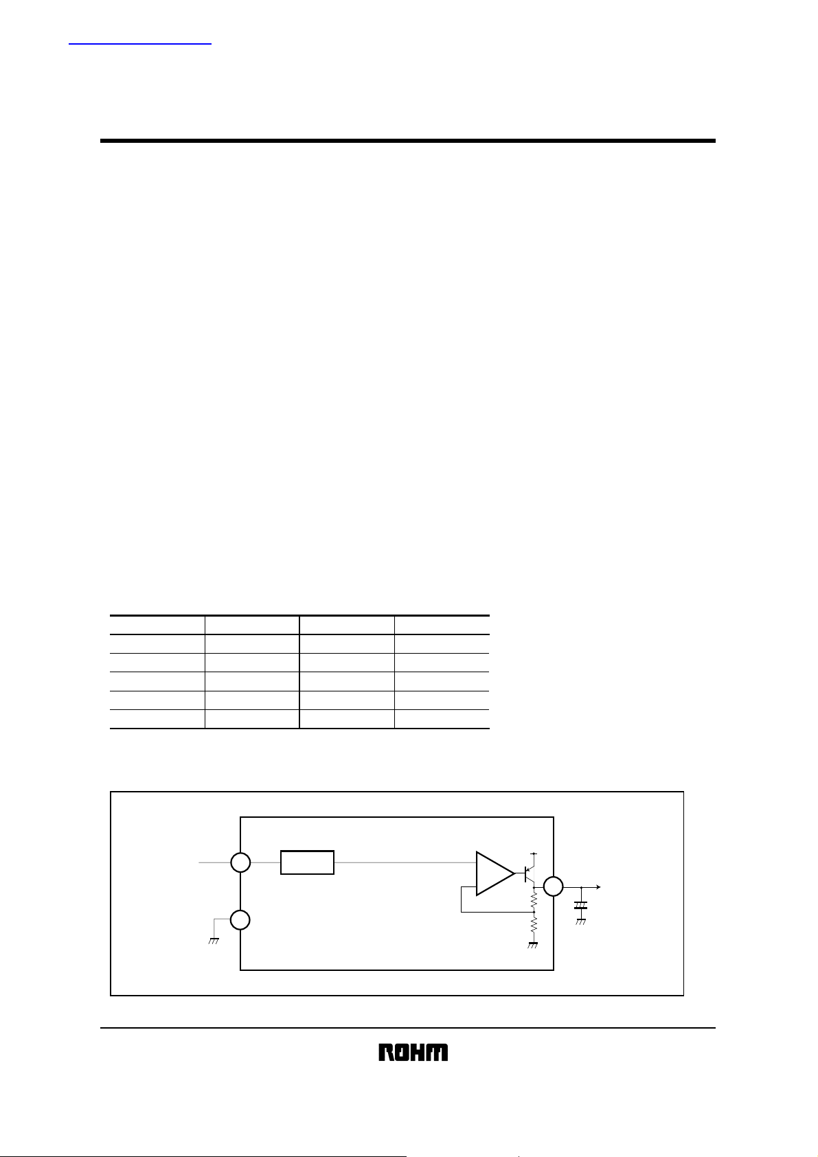
Block diagram
Product No. Product No.
∗∗
CC
V
1
GND
2
Output voltage (V)Output voltage (V)
REFERENCE
VOLTAGE
3) Compatible with the BA178ΟΟ series.
4) Richly diverse lineup.
5) Low minimum I / O voltage differential.
−
+
OUT
3
+
Page 2
Regulator ICs
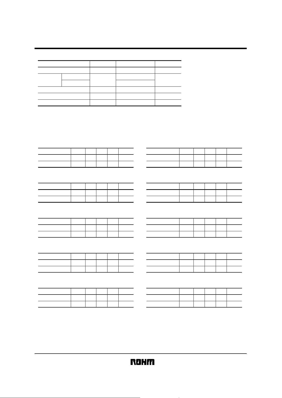
!!!!Absolute maximum ratings (Ta=25°C)
Parameter Symbol Limits Unit
Power supply voltage V
Power
dissipation
TO220FP
TO252 - 3 1000
Operating temperature Topr °C
Storage temperature Tstg °C
Peak applied voltage Vsurge 50
∗1 Reduced by 16mW for each increase in Ta
∗2 Reduced by 8mW for each increase in Ta
∗3 Voltage application time : 200 msec. or less
!!!!
Recommended operating conditions
BA03T / FP
Parameter Symbol Min. Typ. Max. Unit
Input voltage V
Output current Io - - 1 A
IN
CC
Pd
of 1°C over 25°C
of 1°C over 25°C
4 - 25 V
35 V
∗1
2000
∗2
-40~+85
-55~+150
∗3
BA08T / FP
Input voltage V
Output current
Parameter Symbol Min. Typ. Max. Unit
BAOOT / BAOOFP series
mW
V
IN
9 - 25 V
Io - - 1 A
BA033T / FP
Parameter Symbol Min. Typ. Max. Unit
Input voltage V
IN
4.3 - 25 V
Output current Io - - 1 A
BA05T / FP
Parameter Symbol Min. Typ. Max. Unit
Input voltage V
IN
6 - 25 V
Output current Io - - 1 A
BA06T / FP (under development)
Parameter Symbol Min. Typ. Max. Unit
Input voltage V
IN
7 - 25 V
Output current Io - - 1 A
BA07T / FP
Parameter Symbol Min. Typ. Max. Unit
Input voltage V
Output current Io - - 1 A
IN
8 - 25 V
BA09T / FP
Parameter Symbol Min. Typ. Max. Unit
Input voltage V
IN
10-25 V
Output current Io - - 1 A
BA10T / FP
Parameter Symbol Min. Typ. Max. Unit
Input voltage V
IN
11-25 V
Output current Io - - 1 A
BA12T / FP
Parameter Symbol Min. Typ. Max. Unit
Input voltage V
IN
13-25 V
Output current Io - - 1 A
BA15T / FP
Parameter Symbol Min. Typ. Max. Unit
Input voltage V
Output current Io - - 1 A
IN
16-25 V
Page 3
Regulator ICs
!!!!Electrical characteristics
BA03T / FP (unless otherwise noted, Ta=25°C, V
Parameter Symbol Min. Typ. Max. Unit Conditions
Output voltage
Input stability
Ripple rejection ratio
Load regulation
Temperature coefficient of output voltage
Dropout voltage
Bias current
Peak output current
Output short-circuit current
V
O1
Reg.I - 20 100 mV V
R.R. 45 55 - dB Fig.2
Reg.L - 50 150 mV Fig.1
Tcvo
d
V
I
b
O-P
I
Ios
BA033T / FP (unless otherwise noted, Ta=25°C, VCC=8V, IO=500mA)
Parameter
Output voltage
Input stability
Ripple rejection ratio
Load regulation
Temperature coefficient of output voltage
Dropout voltage
Bias current
Peak output current
Output short-circuit current
Symbol Min. Typ. Max. Unit Conditions
V
O1
Reg.I - 20 100 mV V
R.R. 45 55 - dB Fig.2
Reg.L - 50 150 mV Fig.1
Tcvo
d
V
I
b
O-P
I
Ios
=8V, IO=500mA)
CC
2.85 3.0 3.15 V Fig.1
- ±0.02 - Fig.1
- 0.3 0.5 V
- 2.5 5.0 mA
1.0 1.5 - A Tj = 25°C Fig.1
- 0.4 - A
3.13 3.3 3.47 V Fig.1
- ±0.02 - Fig.1
- 0.3 0.5 V
- 2.5 5.0 mA
1.0 1.5 - A Tj = 25°C Fig.1
- 0.4 - A
BAOOT / BAOOFP series
−
IN
= 4→25V Fig.1
eIN = 1V
rms
, f = 120Hz, Io = 100mA
Io = 5mA→1A
Io = 5mA, Tj = 0~125°C
% / °C
Vcc = 0.95V
Io = 0mA
Vcc = 25V
IN
= 4.3→25V Fig.1
eIN = 1V
Io = 5mA→1A
Io = 5mA, Tj = 0~125°C
% / °C
Vcc = 0.95V
Io = 0mA
Vcc = 25V
O
−
rms
, f = 120Hz, Io = 100mA
O
Measurement
circuit
Fig.3
Fig.4
Fig.5
Measurement
circuit
Fig.3
Fig.4
Fig.5
BA05T / FP (unless otherwise noted, Ta=25°C, VCC=10V, IO=500mA)
Parameter
Output voltage
Input stability
Ripple rejection ratio
Load regulation
Temperature coefficient of output voltage
Dropout voltage
Bias current
Peak output current
Output short-circuit current
Symbol Min. Typ. Max. Unit Conditions
V
Reg.I - 20 100 mV V
R.R. 45 55 - dB Fig.2
Reg.L - 50 150 mV Fig.1
Tcvo
4.75 5.0 5.25 V Fig.1
O1
IN
= 6→25V Fig.1
eIN = 1V
rms
, f = 120Hz, Io = 100mA
Io = 5mA→1A
Io = 5mA, Tj = 0~125°C
% / °C
Vcc = 4.75V
Io = 0mA
Vcc = 25V
V
I
O-P
I
Ios
- ±0.02 - Fig.1
d
- 0.3 0.5 V
b
- 2.5 5.0 mA
1.0 1.5 - A Tj = 25°C Fig.1
- 0.4 - A
BA06T / FP (unless otherwise noted, Ta=25°C, VCC =11V, IO= 500mA) (under development)
Parameter
Output voltage
Input stability
Ripple rejection ratio
Load regulation
Temperature coefficient of output voltage
Dropout voltage
Bias current
Peak output current
Output short-circuit current
Symbol Min. Typ. Max. Unit Conditions
V
Reg.I - 20 100 mV V
R.R. 45 55 - dB Fig.2
Reg.L - 50 150 mV Fig.1
Tcvo
V
O-P
I
Ios
5.7 6.0 6.3 V Fig.1
O1
IN
= 7→25V Fig.1
eIN = 1V
rms
, f = 120Hz, Io = 100mA
Io = 5mA→1A
Io = 5mA, Tj = 0125°C
- ±0.02 - Fig.1
d
- 0.3 0.5 V
I
b
- 2.5 5.0 mA
% / °C
Vcc = 0.95V
Io = 0mA
1.0 1.5 - A Tj = 25°C Fig.1
- 0.4 - A
Vcc = 25V
Measurement
circuit
−
Fig.3
Fig.4
Fig.5
Measurement
circuit
−
Fig.3
Fig.4
Fig.5
Page 4

Regulator ICs
BA07T / FP (unless otherwise noted, Ta=25°C, VCC=12V, IO=500mA)
Parameter Symbol Min. Typ. Max. Unit Conditions
Output voltage
Input stability
Ripple rejection ratio
Load regulation
Temperature coefficient of output voltage
V
Reg.I - 20 100 mV V
R.R. 45 55 - dB Fig.2
Reg.L - 50 150 mV Fig.1
Tcvo
Dropout voltage
Bias current
Peak output current
Output short-circuit current
BA08T / FP (unless otherwise noted, Ta=25°C, VCC=13V, IO=500mA)
Parameter Symbol Min. Typ. Max. Unit Conditions
Output voltage
Input stability
Ripple rejection ratio
Load regulation
Temperature coefficient of output voltage
Dropout voltage
Bias current
Peak output current
Output short-circuit current
Reg.I - 20 100 mV V
R.R. 45 55 - dB Fig.2
Reg.L - 50 150 mV Fig.1
Tcvo
6.65 7.0 7.35 V Fig.1
O1
- ±0.02 - Fig.1
d
V
O-P
I
Ios
V
I
- 0.3 0.5 V
b
- 2.5 5.0 mA
1.0 1.5 - A Tj = 25°C Fig.1
- 0.4 - A
7.6 8.0 8.4 V Fig.1
O1
- ±0.02 - Fig.1
d
- 0.3 0.5 V
- 2.5 5.0 mA
1.0 1.5 - A Tj = 25°C Fig.1
- 0.4 - A
I
Ios
V
I
b
O-P
BAOOT / BAOOFP series
−
IN
= 8→25V Fig.1
eIN = 1V
rms
, f = 120Hz, Io = 100mA
Io = 5mA→1A
Io = 5mA, Tj = 0~125°C
% / °C
Vcc = 0.95V
Io = 0mA
Vcc = 25V
IN
= 9→25V Fig.1
eIN = 1V
Io = 5mA→1A
Io = 5mA, Tj = 0~125°C
% / °C
Vcc = 0.95V
Io = 0mA
Vcc = 25V
O
−
rms,
f = 120Hz, Io = 100mA
O
Measurement
circuit
Fig.3
Fig.4
Fig.5
Measurement
Circuit
Fig.3
Fig.4
Fig.5
BA09T / FP (unless otherwise noted, Ta=25°C, VCC=14V, IO=500mA) (under development)
Parameter Symbol Min. Typ. Max. Unit Conditions
Output voltage
Input stability
Ripple rejection ratio
Load regulation
Temperature coefficient of output voltage
Dropout voltage
Bias current
Peak output current
Output short-circuit current
V
Reg.I - 20 100 mV V
R.R. 45 55 - dB Fig.2
Reg.L - 50 150 mV Fig.1
Tcvo
8.45 9.0 9.45 V Fig.1
O1
IN
= 10→25V Fig.1
eIN = 1V
rms,
f = 120Hz, Io = 100mA
Io = 5mA→1A
V
O-P
I
Ios
- ±0.02 - Fig.1
d
- 0.3 0.5 V
b
I
- 2.5 5.0 mA
1.0 1.5 - A Tj = 25°C Fig.1
- 0.4 - A
Io = 5mA, Tj = 0~125°C
% / °C
Vcc = 0.95V
Io = 0mA
Vcc = 25V
O
BA10T / FP (unless otherwise noted, Ta=25°C, VCC=15V, IO=500mA)
Parameter Symbol Min. Typ. Max. Unit Conditions
Output voltage
Input stability
Ripple rejection ratio
Load regulation
Temperature coefficient of output voltage
Dropout voltage
Bias current
Peak output current
Output short-circuit current
V
Reg.I - 20 100 mV V
R.R. 45 55 - dB Fig.2
Reg.L - 50 150 mV Fig.1
Tcvo
V
O-P
I
Ios
9.5 10 10.5 V Fig.1
O1
IN
= 11→25V Fig.1
eIN = 1V
rms
, f = 120Hz, Io = 100mA
Io = 5mA→1A
Io = 5mA, Tj = 0~125°C
- ±0.02 - Fig.1
d
- 0.3 0.5 V
I
b
- 2.5 5.0 mA
% / °C
Vcc = 0.95V
Io = 0mA
1.0 1.5 - A Tj = 25°C Fig.1
- 0.4 - A
Vcc = 25V
Measurement
circuit
−
Fig.3
Fig.4
Fig.5
Measurement
circuit
−
O
Fig.3
Fig.4
Fig.5
Page 5

Regulator ICs
BA12T / FP (unless otherwise noted, Ta=25°C, VCC=17V, IO=500mA)
Parameter Symbol Min. Typ. Max. Unit Conditions
Output voltage
Input stability
Ripple rejection ratio
Load regulation
Temperature coefficient of output voltage
Dropout voltage
Bias current
Peak output current
Output short-circuit current
BA15T / FP (unless otherwise noted, Ta=25°C, VCC=20V, IO=500mA)
Parameter Symbol Min. Typ. Max. Unit Conditions
Output voltage
Input stability
Ripple rejection ratio
Load regulation
Temperature coefficient of output voltage
Dropout voltage
Bias current
Peak output current
Output short-circuit current
V
11.4 12 12.6 V Fig.1
O1
Reg.I - 20 100 mV V
R.R. 45 55 - dB Fig.2
Reg.L - 50 150 mV Fig.1
Tcvo
V
I
b
O-P
I
Ios
V
- ±0.02 - Fig.1
d
- 0.3 0.5 V
- 2.5 5.0 mA
1.0 1.5 - A Tj = 25°C Fig.1
- 0.4 - A
14.25 15 15.75 V Fig.1
O1
Reg.I - 20 100 mV V
R.R. 45 55 - dB Fig.2
Reg.L - 90 200 mV Fig.1
Tcvo
V
I
b
O-P
I
Ios
- ±0.02 - Fig.1
d
- 0.3 0.5 V
- 2.5 5.0 mA
1.0 1.5 - A Tj = 25°C Fig.1
- 0.4 - A
BAOOT / BAOOFP series
−
IN
= 13→25V Fig.1
eIN = 1V
rms
, f = 120Hz, Io = 100mA
Io = 5mA→1A
Io = 5mA, Tj = 0~125°C
% / °C
Vcc = 0.95V
Io = 0mA
Vcc = 25V
IN
eIN = 1V
Io = 5mA→1A
Io = 5mA, Tj = 0~125°C
% / °C
Vcc = 0.95V
Io = 0mA
Vcc = 30V
O
−
= 6→25V Fig.1
rms
, f = 120Hz, Io = 100mA
O
Measurement
circuit
Fig.3
Fig.4
Fig.5
Measurement
circuit
Fig.3
Fig.4
Fig.5
Page 6

Regulator ICs
!!!!Measurement circuits
GND
OUT
22µF
IO
CC
V
VCC
0.33µF
Fig. 1 Measurement circuit for output voltage,
input stability, load regulation,
temperature coefficient of output
voltage
V
BAOOT / BAOOFP series
e
in
V
10Ω5W
100µF
V
CC
0.33µF
eIN = 1Vrms
f = 120Hz
CC
V
Ripple rejection ratio R.R. = 20 log
Fig. 2 Measurement circuit for ripple rejection ratio
GND
OUT
22µF
e
OUT
I
O
=
V
e
IN
)
(
e
OUT
100mA
V
V
CC
= 0.95V
O
0.33µF
CC
V
GND
OUT
22µF
I
O
= 500mA
Fig. 3 Measurement circuit for minimum I/O voltage differential
GND
OUT
22µF
A
I
OS
CC
0.33µF
V
CC
V
Fig. 5 Measurement circuit for
output short-circuit current
GND
OUT
22µF
CC
0.33µF
V
CC
V
A
Fig. 4 Measurement circuit for bias current
Page 7

BAOOT / BAOOFP series
Regulator ICs
!!!!Operation notes
(1) Operating power supply voltage
When operating within the normal voltage range and within the ambient operating temperature range, most circuit
functions are guaranteed.
The rated values cannot be guaranteed for the electrical characteristics, but there are no sudden changes of the
characteristics within these ranges.
(2) Power dissipation
Heat attenuation characteristics are noted on a separate page and can be used as a guide in judging power
dissipation.
If these ICs are used in such a way that the allowable power dissipation level is exceeded, an increase in the chip
temperature could cause a reduction in the current capability or could otherwise adversely affect the performance of
the IC. Make sure a sufficient margin is allowed so that the allowable power dissipation value is not exceeded.
(3) Output oscillation prevention and bypass capacitor
Be sure to connect a capacitor between the output pin and GND to prevent oscillation. Since fluctuations in the valve
of the capacitor due to temperature changes may cause oscillations, a tantalum electrolytic capacitor with a small
internal series resistance (ESR) is recommended.
A 22µF capacitor is recommended; however, be aware that if an extremely large capacitance is used (1000µ F or
greater), then oscillations may occur at low frequencies. Therefore, be sure to perform the appropriate verifications
before selecting the capacitor.
Also, we recommend connecting a 0.33µF bypass capacitor as close as possible between the input pin and GND.
(4) Overcurrent protection circuit
An overcurrent protection circuit is built into the outputs, to prevent destruction of the IC in the even the load is shorted.
This protection circuit limits the current in the shape of a ’7’. This circuit is designed with a high margin, so that that
current is restricted and latching is prevented, even if a high-capacitance capacitator causes a large amount of current
to temporary flow through the IC.
However, these protection circuits are only good for pre-venting damage from sudden accidents and should not be
used for continuous protection (for instance, clamping at an output of 1V
operates). Note that the capacitor has negative temperature characteristics, and the design should take this into
consideration.
(5) Thermal overload circuit
A built-in thermal overload circuit prevents damage from overheating. When the thermal circuit is activated, the
outputs are turned OFF. When the temperature drops back to a constant level, the circuit is restored.
(6) Internal circuits could be damaged if there are modes in which the electric potential of the application’s input (V
GND are the opposite of the electric potential normally used by each of the outputs. Use of a diode or other such
bypass path is recommended.
(7) Although the manufacture of this product includes rigorous quality assurance procedures, the product may be
damaged if absolute maximum ratings for voltage or operating temperature are exceeded. If damage has occurred,
special modes (such as short circuit mode or open circuit mode) cannot be specified. If it is possible that such special
modes may be needed, please consider using a fuse or some other mechanical safety mea-sure.
(8) When used within a strong magnetic field, be aware that the possibility of malfunction exists.
or greater; below 1V
F
, the short mode circuit
F
CC
) and
Page 8

Regulator ICs
!!!!Electrical characteristic curves
25
(1) 22.0
20
15
(2) 11.0
10
(3) 6.5
5
POWER DISSIPATION : Pd (W)
(4) 2.0
0 25 50 75 100 125 150
(Note) When Al thermal plate is used: Tightening torque: 6 (kg-cm) Apply silicon grease
Fig.6 Ta - power dissipation
characteristics (TO220FP)
(1) Infinite heat sink, θ j-c = 5.7 (°C/W)
(2) 100 × 100 × 2 (mm
(3) 50 × 50 × 2 (mm
(4) No heat sink θ j-a = 62.5 (
3
), with Al heat sink
3
), with Al heat sink
°C
/W)
AMBIENT TEMPERATURE : Ta (°C)
12.5
(1) 10.0
10
(1) Infinite heat sink θ j-c=12.5 (°C/W)
(2) IC alone θ j-c=125.0 (°C/W)
7.5
5
2.5
POWER DISSIPATION : Pd (W)
(2) 1.0
0
0 25 50 75 100 125 150
AMBIENT TEMPERATURE : Ta ( °C )
Fig. 7 Ta - power dissipation
characteristics
(TO 252-3)
BAOOT / BAOOFP series
6
5
(V)
OUT
4
3
2
OUTPUT VOLTAGE : V
1
0
25 50 75 100 125 150 175 200
JUNCTION TEMPERATURE : Tj (°C)
Fig. 8 Thermal cutoff circuit
VCC = 10V I
BA05T
characteristics
OUT
= 0
(V)
OUT
10
V
CC
BA05T
= 10V
8
6
(V)
OUT
6
5
4
3
4
2
OUTPUT VOLTAGE : V
0
0 1.0 2.0
OUTPUT CURRENT : I
OUT
Fig. 9 Current limit characteristics
(A)
2
OUTPUT VOLTAGE : V
1
0
01020304050
INPUT VOLTAGE : V
Fig. 10 Over voltage protection
characteristics
!!!!
External dimensions
BA BA
T series
1.8±0.2
−0.2
+0.4
17.0
12.0±0.2
8.0±0.2
5.0±0.2
13.5Min.
2.54±0.5 2.54±0.5 2.6±0.5
+0.3
10.0
−0.1
+0.3
7.0
−0.1
(1)(2)(3)
(Units : mm)
φ3.1±0.1
1.3
0.8
0.55
+0.1
−0.05
4.5
+0.3
−0.1
2.8
(1) V
(2) GND
(3) OUT
+0.2
−0.1
CC
TO220FP
BA05T
CC
(V)
FP series
6.5±0.2
+
0.2
5.0
−
0.1
(2)
7.0±0.3
5.5±0.2
0.8
0.65 0.65
2.3±0.2 2.3±0.2 0.5±0.1
(1) (3)
2.3±0.2
0.5±0.1
(1) V
(2) GND
(3) OUT
9.5±0.5
1.5
2.5
CC
TO252-3
 Loading...