

BA9756FS
Multimedia ICs
High-voltage control circuit for CRT
displays
BA9756FS
The BA9756FS is LSIs that control CRT anode voltage in multi-scan monitors and similar devices, using
a chopper-type voltage control circuit. The internal sawtooth wave generator circuit uses automatic gain control
(AGC) to enable coverage of a wide range from 30kHz to over 150kHz. The BA9756FS is equipped with an internal
high-precision voltage source featuring an output voltage precision of ± 0.7%.
Applications
!
CRT displays, HDTVs, others
Features
!
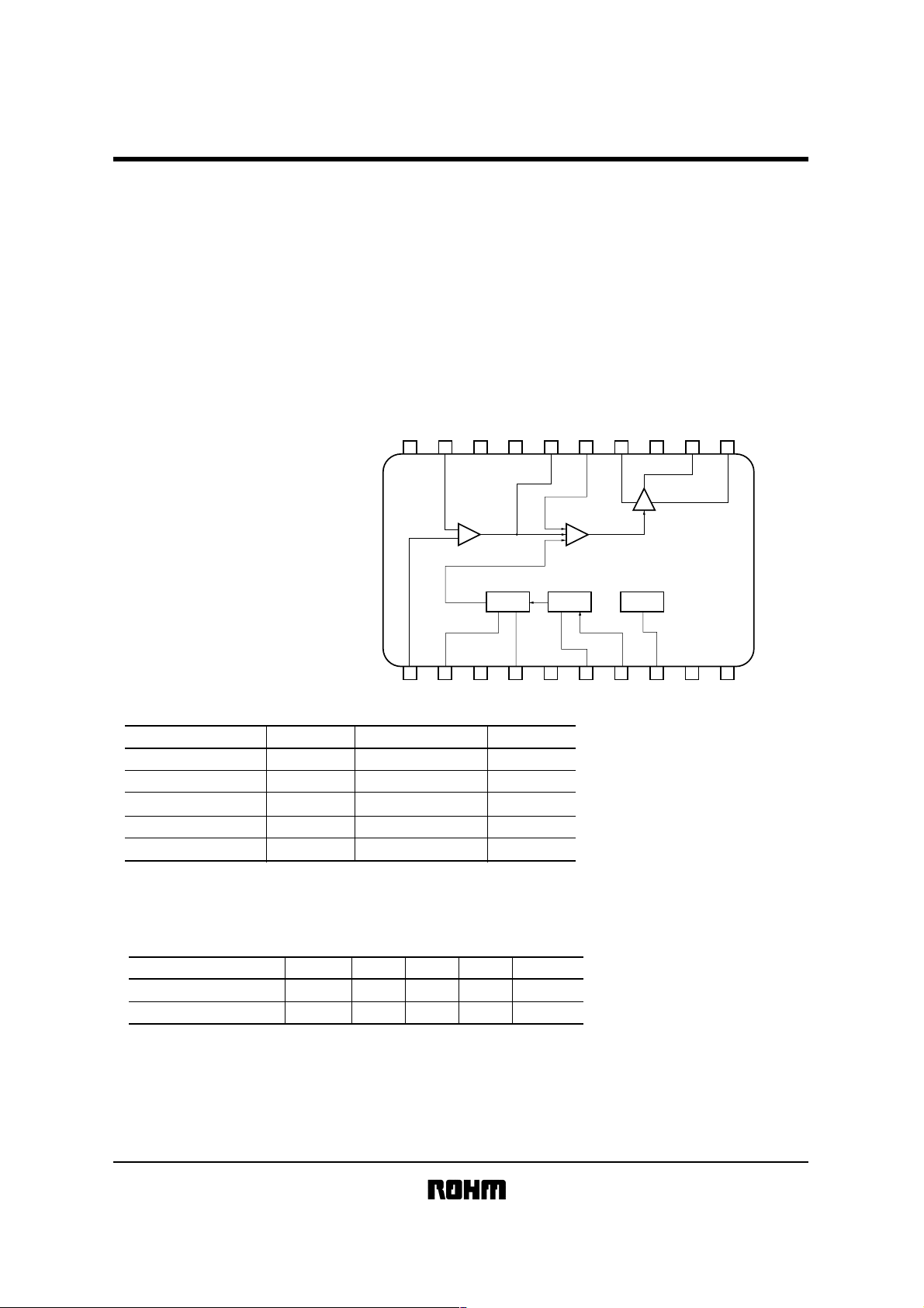
Block diagram
!
20119218317416515614713812911
CC
1V
V
1) Internal chopper-type voltage
control circuit.
2) Internal buffer circuit enables direct
drive of Power MOSFET for output
drive.
3) Internal high-precision voltage
source offers output voltage
precision of ± 0.7%.
Absolute maximum ratings
!
Parameter Symbol Limits Unit
Power supply voltage 1
Power supply voltage 2
Power dissipation
Operating temperature
Storage temperature
When mounted on a 70mm × 70mm × 1.6mm glass epoxy board.
*
1
Reduced by 7.5mW for each increase in Ta of 1˚C over 25˚C.
(Ta=25°C)
V
CC
1
V
CC
2
Pd
Topr
Tstg
18
20
1
*
750
- 25~+80
- 55~+125
CC
2
–
+
SAW GEN.
M / M
+
+
–
9.0V
REF
Buffer
GND
10
V
V
mW
˚C
˚C
Recommended operating conditions
!
Parameter Symbol UnitMax.Typ.Min.
CC
Power supply voltage 1
Power supply voltage 2
V
V
CC
1
2
(Ta=25°C)
11
11
-
-
17
17
V
V

Multimedia ICs
Pin descriptions
!
Pin No. Pin name Function
1
2
3
ERRIN
(error amplifier + input)
AGC
(constant for AGC)
N.C.
SAWOUT
4
(constant for
sawtooth wave)
5
6
N.C.
MMCR
(delay constant for
monostable multivibrator)
7
8
9
10
11
12
13
14
HDIN
(Hd pulse input)
VREF9
(Ref 9V output)
N.C.
GND
(Signal GND)
GND
(Power GND)
PWMOUT
(PWM output)
N.C.
V
CC
2
(Power V
DTC IN
15
(dead time
control input)
16
17
ERROUT
(error amplifier output)
N.C.
18 N.C. See
19
20
1 N.C. pin processing
*
In order to boost the thermal effect of the IC, we recommend connecting this to the GND or to an adjacent pin.
2
*
ERRREF
(error amplifier input)
CC
1
V
CC
(signal V
11 12 14
This is the recovery voltage input pin.
Capacitance should be determined taking into consideration the linearity at the minimum
oscillation frequency, and the response time when the frequency changes.
1
*
.
See
This is the output pin for optimized sawtooth waves, based on the maximum oscillation
frequency.
fMax120kHz C = 1000pF fMax100kHz C = 1200pF
fMax 80kHz C = 1500pF fMax 60kHz C = 2000pF
1
*
.
See
A charging resistance of 4.7kΩ or higher should be used.
The threshold level is 4.5V.
The threshold level is approximately 2.1V.
An output deviation of ± 0.7% is assured through trimming.
1
*
.
See
This may be shared with the power GND, but make sure sufficiently stable grounding
is provided.
This may be shared with the signal GND, but make sure sufficiently stable grounding
is provided.
CC
If a voltage of less than GND or higher than V
is applied because of external back
electromotive force, a protective diode should be inserted (
If the protector circuit and thermal shutdown circuit are tripped, output is fixed at high (V
level.
1
*
See
.
A decoupling capacitor should be positioned in the vicinity of this pin.
CC
)
The voltage input to this pin enables restriction of the PWM output duty.
The duty control is between 0V and 9V, and approximately 0% to 100% is enabled. At 0V,
however, restrictions apply.
The minimum pulse width for the PWM is 0.85µs (Typ. at 90kHz).
This is the output pin for the error amplifier.
1
*
See
.
1
*
.
This is the input pin for the reference voltage.
A decoupling capacitor should be positioned in the vicinity of this pin.
)
V
CC
2
BA9756FS
2
*
).
CC
)
TO FET gate
+

Multimedia ICs
Input / output circuits
!
1
ERRIN
BA9756FS
V
CC
V
CC
V
CC
2
AGC
Fig.1
V
CC
7
6
MMCR
HDIN
V
Fig.2
CC
4
SAW OUT
Fig.3 Fig.4

Multimedia ICs
CC
V
BA9756FS
V
CC
2
14
8
15
DTC
VREG9
11
PGND
Fig.5
V
CC
V
CC
Fig.6
CC
1
V
20
19
ERRREF
12
PWMOUT
10
GND
16
ERROUT
Fig.7 Fig.8 Fig.9

Multimedia ICs
Electrical characteristics
!
BA9756FS
(unless otherwise noted, Ta=25°C, Vcc=15V)
Parameter
<Hd input pin>
Input high level voltage
Input low level voltage
Input high level current
Input low level current
<Monostable multivibrator>
Delay time
<SAW GEN>
Output high level
Output low level
Output level f characteristic
<Reference voltage supply>
Output voltage
Max. output current
Output voltage thermal
characteristics
Thermal shutdown
Symbol Min. Typ. Max. Unit Conditions Test Circuit
V
IH
V
IL
I
IH
I
IL
T
dl
3.0
-
-
-
1.80
-
-
360
0
2.15
V
CC
1.5
530
-1
2.50
V
V
IN
= 15V
V
µA
µA
R = 10kΩ,C = 220pF
µs
-
-
-
Fig.10
Fig.10
Fig.10
Fig.10
Fig.10
H
L
f
V
I
rmax9
T
T
SAW
REF9
REF9
dow
OS
OS
8.0
0
150
8.937
9.0
0.15
200
9.0
10
-
± 0.1
100
10.0
0.35
-
9.063
-
-
± 0.3
-
-
V
V
-1dB drop from 30kHz
kHz
V
mA
Guaranteed design parameter
%
at Ta = 25→0°C, 25→75°C
Guaranteed design parameter
deg
-
-
Fig.10
Fig.10
-
-
—
Fig.10
Fig.10
Fig.10
Fig.10

Multimedia ICs
Measurement circuits
!
BA9756FS
A
20
CC
V
1
6V 1µ
Vs15
2
1
SW15
19
18
17
16
15
14
SW7
7
A
1
V
9.0V
ref
220µ
23
CC
SAW GEN.
2
3
4
+
SW4
1
Vs6
1500p
2
M / M
5
6
2
1
SW6
10k
220p
Fig.10
SG7
+
SW8
1
SW12
V
13
Buffer
8
12
Is12
2
12
11
GND
9
10
V
Is8
Vs19
100k
100k
5k
V
19
2
V
1
1
V
50
16
Fig.11
SW16
1
2
A
CC
6.8k
5.6k
SG1
15µ
100k
+
+
19
16
1
10µ
50
Fig.12
12
SWb
SWa
50
2
1
SWc
SW1
Vs1
1
2

Multimedia ICs
Measurement conditions
!
Parameter
Circuit current
<Error amplifier>
Input bias current
Input offset voltage
Output low level voltage
Output high level voltage
Open voltage gain
Max. output current
<PWM amplifier>
Output high level voltage
Output low level voltage
Rise time
Fall time
Min. pulse width
<HD input pin>
Input high level voltage
Input low level voltage
Input high level current
Input low level current
<Monostable multivibrator>
Delay time
<SAW GEN>
Output high level
Output low level
Output level f
characteristic
(unless otherwise noted, Ta=25°C, Vcc=15V)
1
1
1
1
1
1
1
1
1
1
1
1
1
1
1
1
1
1
3
1
3
1
3
1
3
1
3
1
2
1
1
1
3
2
3
1
3
1
3
1
Switch position
1
1
1
1
1
1
1
1
1
1
1
1
1
1
2
1
2
1
1
1
1
1
1
1
1
1
1
1
1
1
1
1
1
1
1
1
1
1
1
1
Symbol
I
CC
IB
V
IO
V
OL
V
OH
AV
I
OM
V
OH
V
OL
Tr
Td
TMin
V
IH
V
IL
I
IH
I
IL
T
dl
H
OS
L
OS
fsaw
SW1 SW3 SW4 SW5 SW6 SW9 SW11
1
-
1
1
1
1
1
1
1
1
1
1
1
2
2
1
1
1
-
1
1
1
1
-
1
-
1
1
-
1
-
SW12 SWa SWb
1
-
1
1
1
1
1
1
1
1
1
-
1
2
2
-
2
-
1
-
1
-
1
-
1
-
1
-
1
-
1
-
1
-
1
-
1
-
-
1
BA9756FS
SWc
-
-
1
2
2
2
-
2
-
-
-
-
-
-
-
-
-
-
-
-
-
-
1
1
2
2
1
1
1
1
-
-
1
1
-
-
-
-
-
-
-
-
-
-
-
-
-
-
-
-
-
-
-
-
-
-
-
-
-
-
Conditions
-
–5
IN
Vs1 = 6V, IB = - V
Vs1
=
6V, VIO =
×10
(V12 – 6)
×
10
–2
Vs1 = 5V, Vs13 = 6V
Vs1 = 7V, Vs13 = 6V
SG1: f
=
1kHz,VIN =
Vs1 = 7V, Vs13 = 6V
10mV
P-P
*
1
Vs3 = 6V,Vs11 = 5V, Is9 = - 100mA
Vs3 = 6V,Vs11 = 7V, Is9 = ± 100mA
*
SG5: f = 90kHz
SG5
:
f = 90kHz
SG5
:
f = 90kHz
:
f = 90kHz
SG5
SG5
:
f = 90kHz
2
*
2
*
2
*
2
*
2
-
-
*
SG5: f
=
90kHz, Vs4
SG5: f = 90kHz
SG5
:
f = 90kHz
:
f = 30kHz
SG5
=
9V
2
*
2
*
2
*
3
<Reference voltage supply>
-
-
Output voltage
Max. output current
Output voltage thermal
characteristic
V
I
T
Thermal shutdown
1 The pin 12 output amplitude should be set to VO. AV = 20log (VO / VIN) [dB]
*
2 For the method by which the output waveform is determined, refer to Fig. 14.
*
3 An input frequency should be measured that produces a level of -1dB for a high output level (HOS) for the sawtooth waveform at an input frequency of
*
30kHz.
4 The temperature is measured at the point where the temperature is raised to above Ta = 75˚C and the output level of pin 9 is high.
*
REF9
rmax9
REF9
T
dow
-
-
-
-
1
1
-
-
1
1
2
1
1
1
-
-
1
1
1
1
1
1
-
-
1
1
1
1
1
1
-
1
1
1
1
-
-
-
-
Is = – 10mA
-
-
Ta = 0˚C→ 75 ˚C
-
-
Ta = 75˚C
*
4

Multimedia ICs
Application example
!
BA9756FS
Hd in
10kΩ
+
220µF 220pF
10
GND N.C.
REF
9.0V
Buffer
N.C. N.C. N.C. V
11912813714615516417318219120
15V
+
+ B
M / M
–
+
+
1500pF 1µF
N.C. N.C.
HRC
SAW GEN.
+
+
–
+
FBT
CC
15V
+
Anode Voltage
Hd pulse
Note: N.C. pin processing
In order to boost the thermal effect of the IC, we recommend connecting this to the GND or to an adjacent pin.
Fig.13

Multimedia ICs
Input / output waveforms
SG5
(Hd IN)
(SAW OUT)
3.0V
1.5V
H
OS
L
100%
90%
BA9756FS
OS
External dimensions
!
BA9756FS
20
7.8 ± 0.3
5.4 ± 0.2
1
1.8 ± 0.1
0.11
(PWM OUT)
8.7 ± 0.2
(Units: mm)
11
10
0.36 ± 0.10.8
SSOP-A20
0.3Min.
0.15 ± 0.1
0.15
TMin.TdlTd
Fig.14
50%
10%
0%
Tr
 Loading...