

Page 1
Serial-in / Parallel-out Driver Series
Serial / Parallel
5-input Driver
BA829
No.09051EAT02
●Description
Serial-in-parallel-out driver is a constant-current output driver with a built-in shift register and a latch circuit to turn on a
maximum of 8 LED by a 5-line interface linked to a microcontroller. Output current value of constant-current can be set up to
a maximum of 300mA.
●Features
1) This product can drive a maximum of 300mA.
2) When the strobe terminal is controlled by the drive timing pulse, current during a period without driving can be reduced.
3) When the data output terminal is used as the next input data, cascade connection becomes possible.
4) Digital ground and power ground are separated.
5) Latch is built in between the shift register and the driver output.
6) Stand-by function is incorporated. (10μA Typ. upon standby)
●Applications
For AV equipment such as, component stereo sets, videos and TV sets, PCs, and control microcontroller mounted equipment.
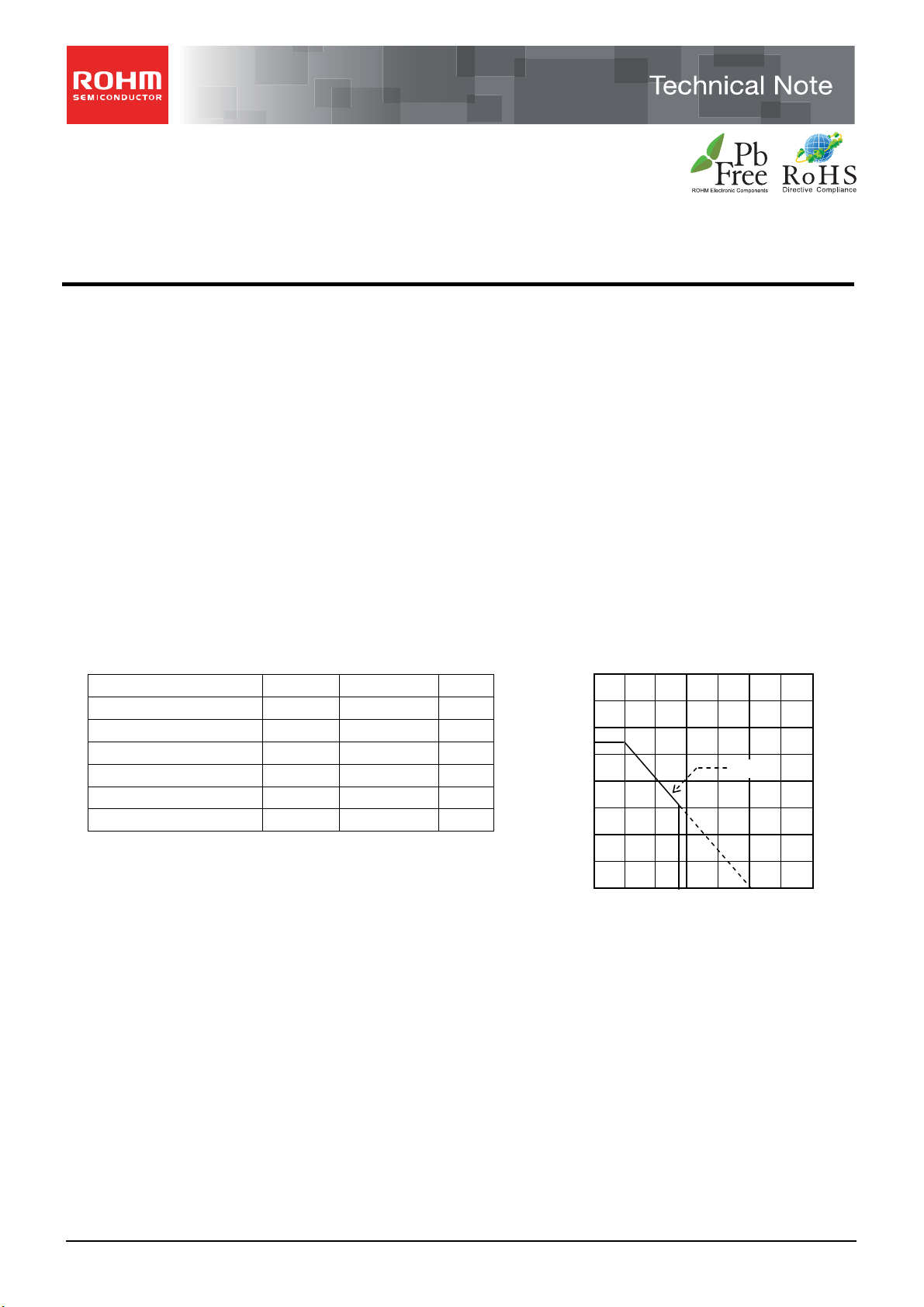
●Absolute maximum ratings ●Thermal derating curve
Parameter Symbol Limit Unit
1600
1400
Power supply voltage VDD -0.3 to +7.0 V
Power dissipation Pd 1100* mW
Input voltage ISINK -0.3 to VCC V
Output voltage VO 15 V
Operating temperature Topr -25 to +70 ℃
Storage temperature Tstg -55 to +125 ℃
*1 Reduced by 11 mW/C over 25C.
1200
1000
800
600
400
Power dissipation Pd 〔mW〕
200
0
70℃
50 75 25 100 125 150 175
Ambient temperature Ta 〔℃〕
BA829
www.rohm.com
© 2009 ROHM Co., Ltd. All rights reserved.
1/7
2009.06 - Rev.A
Page 2

BA829
Technical Note
●Recommended operating conditions (Topr=-25℃ to +70℃)
Parameter
Symbol Min. Typ. Max. Unit Condition
Power supply VCC 4.5 5.0 5.5 V Clock frequency TCLK - - 500 kHz Power setup time tPset 500 - - ns Fig.4
Clock pulse width tWC 1 - - ns Fig.4
Data setup time tDset 300 - - ns Fig.4
Data hold time tDhold 400 - - ns Fig.4
Latch pulse timing 1 tLT1 600 - - ns Fig.4
Latch pulse timing 2 tLT2 250 - - ns Fig.4
Latch pulse width tWL 800 - - ns Fig.4
Strobe pulse timing 1 tST1 300 - - ns Fig.4
Strobe pulse width tws 3 - - μs Fig.4
Voltage between L-GND and P-GND VG - - 0.2 V -
* Electric potential is a difference of L-GND and P-GND. Short-circuit near the power source whenever possible.
However, between L-GND Pin and P-GND Pin, product should be used in a range not exceeding 0.2V.
●Electrical characteristics (Unless otherwise specified, Ta=25℃,VCC=5.0V)
Parameter Symbol Min. Typ. Max. Unit Condition Test Circuit
Supply current 1 Icc1 - 10 20 μA PSW“L” Fig.1
Supply current 2 Icc2 - 110 158 mA PSW“H”, STB“H” Fig.1
Supply current 3 Icc3 - 14 20 mA PSW“H”, STB“L” Fig.1
Output ON voltage VOON - 0.4 0.6 V ICCN=300 mA Fig.1
Output leakage current IOOFF - 10 50 μA V0=13.5V Fig.1
Data transference time fCLK 500 - - kHz - Fig.1
Input high-level voltage VIH 2.6 - - V - Fig.2
Input low-level voltage VIL - - 0.8 V - Fig.2
1=3.4V,CLK,LATCH
Input high-level current IIH1 - 0.1 10 μA
Input low-level current IIL1 - -0.01 -0.1 mA
V
,DATA,STB
1=0.4V,CLK,LATCH
V
,DATA,STB
Fig.1
Fig.1
Out put high-level voltage VDDH 2.8 3.0 - V IDOH=-400μA Fig.1
Output low-level voltage VDDL - 0.3 0.4 V IDOL=⊿1.6mA Fig.1
Data output transmission delay tDLH - 0.6 1.0 μs RLD=10kΩ Fig.4
Data output transmission delay tDHL - 0.6 2.0 μs RLD=10kΩ Fig.4
R
Print output transmission delay tOLH - - 10 μs
Print output transmission delay tOHL - - 10 μs
L=560kΩ560,
V
0=13.5V
L=560kΩ560,
R
0=13.5V
V
Fig.4
Fig.4
Input high-level current IIH2 - 0.04 0.1 mA V1=3.4V,PSW Fig.1
Input low-level current IIL2 - 0.1 10 μA V1=0.4V,PSW Fig.1
www.rohm.com
© 2009 ROHM Co., Ltd. All rights reserved.
2/7
2009.06 - Rev.A
Page 3

BA829
●Block diagram
Pulse Gen.
Technical Note
×8
DOFF
V
LD
STB
PSW
PAW
L
R
PGND
Fig.1
Fig.2
A
08
PGND
LGND Vcc
LGND V
V
A
V
OON
V
01
A
I
CC1~3
V
CC
CC
V
CC
O
W
V
DCH
V
V
DCL
CLK
R
Do
CLK
DATA
LATCH
DATA
LATCH
STB
A
I
IIH IIIL
VI
www.rohm.com
© 2009 ROHM Co., Ltd. All rights reserved.
3/7
2009.06 - Rev.A
Page 4

BA829
Technical Note
●Block diagram
03
13
12
11 0410
05
06
07
08
9
8
7
6
01
02
POWER
PGND
14
5
GND
STB
LATCH
CLK
DATA
17
18
16
LATCH
SHIFT REG
1
V
4
CC
LOGIC
15
GND
3
D
OUT
POWER ON
2
PSW
Fig.3
●Pin descriptions
PIN No. Terminal I/O Function
1 CLK I Clock input
2 PSW I Power switch
3 DOUT O Cascade output
4 VCC - Power supply
5 PGND - GND
6 O8 O
7 O7 O
8 O6 O
9 O5 O
10 O4 O
Parallel data output
11 O3 O
12 O2 O
13 O1 O
14 PGND - GND
15 LGND - GND
16 DATA I Serial data input
17 STB I Strobe input , “L” active
18 LATCH I Latch input
●Description of operation
BA829 is configured internally as shown in the logic circuit diagram. Terminals of clock (CLK), data (DATA), latch (LATCH),
strobe (STB), and power switch (PSW) are available as input.
Data input is synchronized with the clock, read serially during the rise time and latched at the rise time edge of the shifted
shift register. Latched data appears on the output terminal of O1-O8 by the strobe input. Pulse width is the same as that of
the strobe input. Data output terminal DOUT, is a terminal used for cascade connection of the IC, where the output of the
final stage of the shift register has appeared, and is connected to the next data input terminal DATA. In this case, when the
clock and the strobe are used in conjunction, output terminal can be increased by 8 bits at a time.
To affect the standby mode, set the power switch to “L”.
www.rohm.com
© 2009 ROHM Co., Ltd. All rights reserved.
4/7
2009.06 - Rev.A
Page 5

BA829
●Timing chart
PSW
CLK
DATA
Pset
t
twc twc
t
~ ~
1 2 8 9 10
~ ~
Dset tDhold
~ ~
tDLH
tDHL
Technical Note
D
OUT
LATCH
STB
OB
●Interfaces
VCC
(a) INPUT (CLK , DATA , LATCH , STB)
IL
Fig.4
(b) INPUT (PSW)
~
~
tLT1 tLT2
~
~
tWL tWL
~
~
~
~
V
CC
tST1
tWS
tDHL tDLH
I
L
~
~
(c) OUTPUT (D
OUT
V
CC
)
www.rohm.com
© 2009 ROHM Co., Ltd. All rights reserved.
5/7
2009.06 - Rev.A
Page 6

P
iti
P
iti
BA829
Technical Note
●Operation Notes
1. Absolute maximum ratings
An excess in the absolute maximum ratings, such as supply voltage, temperature range of operating conditions, etc., can break
down the devices, thus making impossible to identify breaking mode, such as a short circuit or an open circuit. If any over rated
values will expect to exceed the absolute maximum ratings, consider adding circuit protection devices, such as fuses.
2. Connecting the power supply connector backward
Connecting of the power supply in reverse polarity can damage IC. Take precautions when connecting the power supply
lines. An external direction diode can be added.
3. Power supply lines
Design PCB layout pattern to provide low impedance GND and supply lines. To obtain a low noise ground and supply line,
separate the ground section and supply lines of the digital and analog blocks. Furthermore, for all power supply terminals
to ICs, connect a capacitor between the power supply and the GND terminal. When applying electrolytic capacitors in the
circuit, note that capacitance characteristic values are reduced at low temperatures.
4. GND voltage
The potential of GND pin must be minimum potential in all operating conditions.
5. Inter-pin shorts and mounting errors
Use caution when positioning the IC for mounting on printed circuit boards. The IC may be damaged if there is any
connection error or if pins are shorted together.
6. Actions in strong electromagnetic field
Use caution when using the IC in the presence of a strong electromagnetic field as doing so may cause the IC to malfunction.
7. Testing on application boards
When testing the IC on an application board, connecting a capacitor to a pin with low impedance subjects the IC to stress.
Always discharge capacitors after each process or step. Always turn the IC's power supply off before connecting it to or
removing it from a jig or fixture during the inspection process. Ground the IC during assembly steps as an antistatic
measure. Use similar precaution when transporting or storing the IC.
8. Regarding input pin of the IC
This monolithic IC contains P+ isolation and P substrate layers between adjacent elements in order to keep them isolated.
P-N junctions are formed at the intersection of these P layers with the N layers of other elements, creating a parasitic diode
or transistor. For example, the relation between each potential is as follows:
When GND > Pin A and GND > Pin B, the P-N junction operates as a parasitic diode.
When GND > Pin B, the P-N junction operates as a parasitic transistor.
Parasitic diodes can occur inevitable in the structure of the IC. The operation of parasitic diodes can result in mutual
interference among circuits, operational faults, or physical damage. Accordingly, methods by which parasitic diodes
operate, such as applying a voltage that is lower than the GND (P substrate) voltage to an input pin, should not be used.
Pin A
N
P+ P
Parasitic element
P
GND
Resistor Transistor (NPN)
B
C
E
N
P
P substrate
GND
+
N N
P substrate
Pin A
aras
element
Pin B
N
c
Parasitic element
P+
Fig.5 Example of IC structure
P+
N
GND
Pin B
B C
E
Other adjacent elements
9. Ground Wiring Pattern
When using both small signal and large current GND patterns, it is recommended to isolate the two ground patterns,
placing a single ground point at the ground potential of application so that the pattern wiring resistance and voltage
variations caused by large currents do not cause variations in the small signal ground voltage. Be careful not to change the
GND wiring pattern of any external components, either.
GND
aras
element
c
www.rohm.com
© 2009 ROHM Co., Ltd. All rights reserved.
6/7
2009.06 - Rev.A
Page 7

BA829
●Ordering part number
B D 8 2 9
Technical Note
Part No. Part No.
DIP18
0.51Min.
3.95±0.3
3.29±0.2
22.9±0.3
18
19
2.54
Package
None:DIP18
Packaging and forming specification
None: Tube
<Tape and Reel information>
10
0.5±0.1
6.5±0.3
7.62
0°−15°
Quantity
Direction of feed
0.3±0.1
(Unit : mm)
TubeContainer
1000pcs
Direction of products is fixed in a container tube
Order quantity needs to be multiple of the minimum quantity.
∗
www.rohm.com
© 2009 ROHM Co., Ltd. All rights reserved.
7/7
2009.06 - Rev.A
Page 8

Notes
No copying or reproduction of this document, in part or in whole, is permitted without the
consent of ROHM Co.,Ltd.
The content specied herein is subject to change for improvement without notice.
The content specied herein is for the purpose of introducing ROHM's products (hereinafter
"Products"). If you wish to use any such Product, please be sure to refer to the specications,
which can be obtained from ROHM upon request.
Examples of application circuits, circuit constants and any other information contained herein
illustrate the standard usage and operations of the Products. The peripheral conditions must
be taken into account when designing circuits for mass production.
Great care was taken in ensuring the accuracy of the information specied in this document.
However, should you incur any damage arising from any inaccuracy or misprint of such
information, ROHM shall bear no responsibility for such damage.
The technical information specied herein is intended only to show the typical functions of and
examples of application circuits for the Products. ROHM does not grant you, explicitly or
implicitly, any license to use or exercise intellectual property or other rights held by ROHM and
other par ties. ROHM shall bear no responsibility whatsoever for any dispute arising from the
use of such technical information.
Notice
The Products specied in this document are intended to be used with general-use electronic
equipment or devices (such as audio visual equipment, ofce-automation equipment, communication devices, electronic appliances and amusement devices).
The Products specied in this document are not designed to be radiation tolerant.
While ROHM always makes ef forts to enhance the quality and reliability of its Products, a
Product may fail or malfunction for a variety of reasons.
Please be sure to implement in your equipment using the Products safety measures to guard
against the possibility of physical injury, re or any other damage caused in the event of the
failure of any Product, such as derating, redundancy, re control and fail-safe designs. ROHM
shall bear no responsibility whatsoever for your use of any Product outside of the prescribed
scope or not in accordance with the instruction manual.
The Products are not designed or manufactured to be used with any equipment, device or
system which requires an extremely high level of reliability the failure or malfunction of which
may result in a direct threat to human life or create a risk of human injury (such as a medical
instrument, transportation equipment, aerospace machinery, nuclear-reactor controller,
fuel-controller or other safety device). ROHM shall bear no responsibility in any way for use of
any of the Products for the above special purposes. If a Product is intended to be used for any
such special purpose, please contact a ROHM sales representative before purchasing.
If you intend to export or ship overseas any Product or technology specied herein that may
be controlled under the Foreign Exchange and the Foreign Trade Law, you will be required to
obtain a license or permit under the Law.
www.rohm.com
© 2009 ROHM Co., Ltd. All rights reserved.
Thank you for your accessing to ROHM product informations.
More detail product informations and catalogs are available, please contact us.
ROHM Customer Support System
http://www.rohm.com/contact/
R0039
A
 Loading...