

1
Video ICs
VCR standard audio signal processor
BA7797F
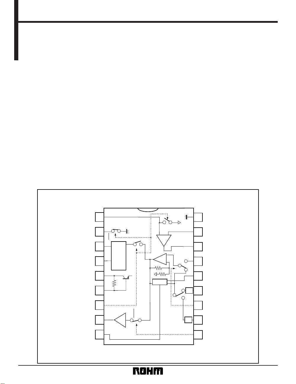
The BA7797F is standard audio signal processor designed for use in VCRs and tape decks. The circuit is comprised
of a playback preamplifier, a line amplifier, a recording amplifier, an ALC circuit and high-voltage head switch.
The IC has a built-in coil equivalent circuit for recording equalization, which eliminates the need for an external component.
•
Applications
Video cassette recorders and tape decks
•
Features
1) Two input switching systems built-in (LINE and TUNER).
2) Built-in coil equivalent circuit for recording equalization.
3) High-performance low-noise playback amplifier.
4) ALC level can be adjusted by connection of an
external resistor.
5) Compatible with single-mode EQ making it ideally
suited to widely-used decks.
•
Block diagram
LINE
ALC
PB
REC
REC
0dB
EQ
REC AMP
BUFF
MUTE
1
2
3
4
5
6
7
8
9
10
11
12
13
14
15
16
17
18
GND
+ 28dB
V
CC
PB IN
REC HEAD SW
REC OUT
REC L
RIPPLE FILTER
REC / EE CTRL
LINE OUT
ALC LEVEL ADJ
PB NFB
PB OUT
PB LINE IN
ALC FILTER
TUNER IN
PB / TU / LINE CTRL
LINE IN
MUTE CTRL
ATT
– 8dB
ATT
– 8dB
2
Video ICs BA7797F
•
Absolute maximum ratings (Ta = 25°C)
Parameter Symbol Limits Unit
V
CC 13 V
550
∗
mW
Topr °C
Tstg °C
Pd
– 10 ~ + 65
– 55 ~ + 125
Power supply voltage
Power dissipation
Operating temperature
Storage temperature
∗
When mounted on a 50mm × 50mm × 1.6mm glass epoxy board. Reduced by 5.5mW for
each increase in Ta of 1°C over 25°C.
•
Recommended operating conditions (Ta = 25°C)
Parameter
Symbol
Min. Typ. Max. Unit
V
CC
7.5 — 12.5 V
Power supply voltage
•
Pin descriptions (VCC = 10V)
1 PB IN 2.0V
REC: 120kΩ
REC: 11Ω
2 REC HEAD SW 0.0V
REC: OPEN
3 REC OUT 4.7V EF (P-P)
4 REC L 4.7V B (NPN)
5
V
CC
10.0V —
6 RIPPLE FILTER 10.0V 10kΩ (V
CC)
7 REC / EE CTRL —
8 LINE OUT 4.7V EF (P-P)
9 ALC LEVEL ADJ 4.1V
10 MUTE CTRL —
11 LINE IN 4.7V 120kΩ
12 PB / TU / LINE CTRL —
13 TUNER IN 4.7V 120kΩ
14 ALC FILTER
PB: 0.0V
15 PB LINE IN 4.7V 120kΩ
16 PB OUT 2.0V EF (P-P)
17 PB NFB 2.0V B (NPN)
18 GND 0.0V —
Pin No. Pin name Function Pin voltage I / O circuit
REC: 17Ω (ON)
EF (NPN) ~ 100Ω
PB: Not fixed
See input / output circuit
See Fig. 4
See input / output circuit
See input / output circuit
Playback amplifier input / playback head switch
High-withstanding voltage recording head switch
Recording amplifier output
Recording EQ switch
V
CC
Ripple filter
REC / EE control
Line amplifier output
ALC level adjustment
Mute control
Line input
PB / TU / LINE control
Tuner input
For setting the time constant for the ALC filter
(attack and recovery times)
Line input for playback
Playback amplifier output
Playback amplifier feedback
GND
∗
EF: emitter follower, P-P: push pull, B: base, and C: collector.
All measurements made using the measurement circuit (Fig.1) with V
CC = 10V and quiescent circuit conditions.
All numerical values are standardized values.

3
Video ICs BA7797F
•
Input / output circuits
H
L
CTRL
56kΩ
REC
AMP
PB
HEAD SW
7
REC / EE
REC / EE CTRL 7
M
56kΩ
MUTE
CTRL
10
MUTE CTRL 10
H
L
56kΩ
CTRL
12
PB / TU / LINE CTRL 12
PB / TU / LINE

4
Video ICs BA7797F
•
Electrical characteristics (unless otherwise noted, Ta = 25°C, VCC = 10V, and f = 1kHz)
Parameter Symbol Min. Typ. Max. Unit Conditions
I
qEE 6.4 8.5 11.3 mA
I
qPB 6.4 8.5 11.3 mA
I
qREC 5.2 6.9 9.2 mA
G
VCLP 27.0 28.0 29.0 dB
G
VCLT 19.0 20.0 21.0 dB
THD
LT — 0.1 0.3 %
V
OMLT 5.9 8.4 — dBV
V
NOLT —
– 81.5
– 75 dBV
V
OA – 9.0 – 8.0 – 7.0 dBV
THD
A — 0.1 0.5 %
MT —
– 82.0
– 72 dB
G
VCR 19.0 20.0 21.0 dB
THD
R — 0.13 0.4 %
V
OMR 5.7 8.2 — dBV
G
VOR 60 71 — dB
G
VOP 61 68 — dB
V
NINP — – 122.5 – 114 dBV
G
VCP 35.0 36.0 37.0 dB
R
PH —1120Ω
R
RH —1725Ω
BV
RHDC —010µAE2 = ± 55V
BV
RHAC 80 100 — V
P-P
Measurement
circuit
Fig.1
Fig.1
Fig.1
Fig.1
Fig.1
Fig.1
Fig.1
Fig.1
Fig.1
Fig.1
Fig.1
Fig.1
Fig.1
Fig.1
Fig.1
Fig.1
Fig.1
Fig.1
Fig.1
Fig.1
Fig.1
V
O = – 8dBV
V
O = – 8dBV
V
O = – 8dBV, RL = 4.7kΩ
∗
THD = 1%, RL = 4.7kΩ
∗
VO = 0dBV, DIN AUDIO
LINE IN, TUNER IN→REC OUT
VO = – 8dBV
V
IN = – 25dBV, RL = 4.7kΩ
∗
VO = – 8dBV, RL = 4.7kΩ
∗
THD = 1%, RL = 4.7kΩ
∗
Rg = 680Ω, DIN AUDIO
PB IN→PB OUT
f = 70kHz, V
2 ⬉ ± 1.5V
Rg = 4.7kΩ, DIN AUDIO
V
IN = – 25dBV, 9pin: OPEN
Fig.2
∗
Measured at BW = 400Hz to 30kHz.
Quiescent current EE
Quiescent current PB
Quiescent current REC
〈Line amplifier〉
Voltage gain (PB input)
Voltage gain (LINE1, LINE2, TU inputs)
Distortion
Maximum output level
Output residual noise
ALC level
ALC distortion
Mute attenuation ratio
〈Recording amplifier〉
Voltage gain
Distortion
Maximum output level
Openloop gain
Playback preamplifier
Openloop gain
Input conversion noise
Voltage gain (stand alone)
〈Head switch〉
PB head switch impedance
REC head switch impedance
REC head switch DC withstanding voltage
REC head switch AC withstanding voltage
No signal
No signal
No signal

5
Video ICs BA7797F
•
Measurement circuits
1
2
3
4
5
6
7
8
9
18
17
16
15
14
13
12
11
10
4.7µ
4.7k
1.5k
12k
6000p
22µ
CTRL
4.7k
4.7k
0.1µ
47k
4.7k
0.1µ
47k
2.2M
22µ
4.7k
0.1µ
47k
TUNER IN
22µ
330
0.01µ
4.7k
12k
330k
4.7µ
4.7µ
REC AMP
EQ
0dB
ALC
LINE
3.3µ
68k
680
PB IN
REC HEAD SW
REC OUT
VCC
33µ
REC / EE
LINE OUT
BUFF
MUTE
PB
REC
ON: Gvo PB
PB OUT
PB LINE IN
ON: ALC OFF
PB / TU / LINE CTRL
LINE IN
MUTE CTRL
REC
ATT
– 8dB
ATT
– 8dB
+ 28dB
1800p
Units: R [Ω]
C [F]
Fig.1
+
+
+
+
+
+
+
+
REC head switch AC withstanding voltage measurement circuit
Fig. 2
1
REC
V
V
2
3
0.1µ
0.1µ
BVRHAC
V2
e2
100k
100k 1k
SW
2
REC OUT
PB IN
~

6
Video ICs BA7797F
Control pins
(1) REC / EE control, PB / TU / LINE control
Function
L L LINE OFF ON LINE OFF
L M TUNER OFF ON TUNER OFF
L H PB OFF ON PB OFF
H L ON OFF LINE ON
H M ON OFF TUNER ON
H H inhibit————
REC / EE PB / TU / LINE PB HSW REC HSW LINE SW REC AMP
LINE REC
TU REC
Mode
If REC / EE CTRL is set to "M", the REC pause state is possible (REC head switch: open, REC amplifier: off).
•
Control mode table
MUTE
H MUTE OPEN
L MUTE CLOSE
LINE SW
Mode
Control pins Function
(2) Mute control
•
Application example
12k
330k
330
REC + B
LINE
ALC
PB
REC
REC
0dB
BIAS
OSC
EQ
REC AMP
0.1µ
RL
CTRL
BUFF
MUTE
8.2k
1
2
3
4
5
6
7
8
9
10
11
12
13
14
15
16
17
18
3.3µ
22µ0.01µ
REC / EE
+ 28dB
VCC
ATT
– 8dB
ATT
– 8dB
EQ CTRL
TUNER IN
PB / TU / LINE CTRL
LINE IN
MUTE CTRL
ALC LEVEL ADJ
LINE OUT
EQ CTRL
22µ
33µ
0.1µ 0.1µ
Units: R [Ω]
C [F]
Fig.3
+
+
+
+
+
+
+

7
Video ICs BA7797F
•
Operation notes
(1) ALC level
Set the ALC level in the range – 8dBV to 0dBV by connecting a resistor between pin 9 and GND.
The formula for approximating the value of this resistor
is as follows:
When pin 9 is open, V
OA is preset to – 8dBV (for VCC =
10V).
Note that the supply voltage V
CC has an effect.
(2) Mute signal
Apply the mute signal shown below at power on and off.
If the muting time is short, a “pop” sound will be audible, particularly when the power is switched on.
9
ALC LEVEL
R
4k
32k
V
BIAS
ALC DET
ADJ
Fig.4
(H)
(H)
V
CC
MUTE CTRL
LINE OUT
Fig.5
2 sec. Min.
Also, be certain to apply the mute signal when switching between PB / LINE / TU. In the case of LINE / TU
switching, it is possible to suppress switching noise by
applying a time constant to the signal, in which case it
is not necessary to apply the mute signal.
(3) Recording control
Do not switch the PB and REC modes on together.
This will cause faulty operation.
(4) Line output
The line output can drive a load resistance of up to 2kΩ.
Depending on the type of load, it can cause local oscillation (eg. large capacitive loads that draw large current), so caution is required. In particular, when there is
a possibility that the line output will be connected to a
shielded cable, or line cable, connect a resistor of about
1kΩ in series with the output so that the capacitive load
is not directly coupled to the IC output terminal.
2
VCC – 0.7
• V
BIAS
VOA = •
2
•
1
4k
4k + 32k × R / (32k + R)
2
1
•
4k
4k + 32k × R / (32k + R)
=
2
VCC – 0.7
• V
BIAS
VBIAS =
32k × R / (32k + R)
4k + 32k × R / (32k + R)
9pin Voltage =

8
Video ICs BA7797F
•
Electrical characteristic curves
10 100 1k 10k 100k 1M
20
40
50
60
30
VCC = 10V
V
IN = – 60dBV
0.01µ
22µ
330k 12k
1617
+
+
–
PB
330
GAIN: GV (dB)
FREQUENCY: f (Hz)
10M
Fig. 6 Gain vs. frequency (PB amplifier)
MAXIMUM OUTPUT LEVEL: Vom (dBV)
LOAD RESISTANCE: RL (Ω)
100 200 500 1k 2k 5k 10k
0
2
4
6
8
10
10µ
+
LINE
VOUT
RL
VCC = 10V
THD = 1%
ALC OFF
(BW = 0.4 ~ 30kHz)
Fig. 7 Line amplifier load drive
characteristics
OUTPUT LEVEL: VOUT (dBV)
INPUT LEVEL: VIN (dBV)
–40
–20
–10
00
10
–30
–30 –20 –10 00
VCC = 10V
VCC = 8.58V
f = 1kHz
Input: LINE IN
Output: LINE OUT
Fig. 8 ALC input / output characteristics
GAIN GVR: (dB)
FREQUENCY: f (Hz)
100
10
20
30
40
50
1k 10k 100k
V
CC = 10V
REC
&EQ
12k
+
1.5k
1800p 6000p
4
3
OUT
10µ
4.7k
Input: LINE IN
Output: REC OUT
Fig. 9 Gain vs. frequency (REC amplifier)
•
External dimensions (Units: mm)
SOP18
0.4 ± 0.11.27
0.3Min.
0.11
1.8 ± 0.1
5.4 ± 0.2
7.8 ± 0.3
0.15 ± 0.1
18
1
11.2 ± 0.2
10
9
0.15
 Loading...