ROHM BA7630S, BA7630F Datasheet

1
Multimedia ICs
Video switch for CANAL-Plus decoder
BA7630S / BA7630F
The BA7630S and BA7630F are decoder switching ICs for the scrambled broadcasts in France. The ICs include a 3input multiplexer, 2-input multiplexers with 6dB amplifiers, and a 9-bit serial-to-parallel converter.
These ICs greatly simplify decoder switching, and can be connected to a control microprocessor using just two lines.
•
Applications
Video cassette recorders
•
Features
1) All the switching functions required for SECAM
CANAL plus decoder integrated onto one chip.
2) Built-in 9-bit serial-to-parallel converter for decoder
and TV control reduces number of microprocessor
wiring connections required.
3) Inputs have a sync-tip clamp.
4) The switch section can be used independently.
5) Low power consumption off a 5V supply.
•
Absolute maximum ratings (Ta = 25°C)
Parameter Symbol Limits Unit
V
CC
9
∗
1
V
BA7630S 500
∗
2
mW
BA7630F 600
∗
3
Topr – 25 ~ + 70 °C
Tstg – 55 ~ + 125 °C
Pd
Power supply voltage
Power dissipation
Operating temperature
Storage temperature
∗
1 13V for switches 1 to 9.
∗
2 Reduced by 5.0mW for each increase in Ta of 1°C over 25°C.
∗
3 Reduced by 6.0mW for each increase in Ta of 1°C over 25°C.
•
Recommended operating conditions (Ta = 25°C)
Parameter Symbol Min. Typ. Max. Unit
V
CC 4.5 5.0 5.5 VPower supply voltage

2
Multimedia ICs BA7630S / BA7630F
•
Pin descriptions
Pin No. Pin No.
1 IN 4 OUT 2
2 GND
3 IN 1
4 (5) RESET IN SW 5 OUT
5 (6) IN 2 SW 6 OUT
GND SW 7 OUT
IN 3 SW 8 OUT
SW 1 IN / OUT CLOCK IN
SW 2 IN / OUT DATA IN
SW 3 IN / OUT SW 9 OUT
OUT 3 OUT 1
6 (7)
7 (8)
8 (9)
9 (10)
10 (13)
11 (14)
V
CC
SW 4 IN / OUT
12 (15)
13 (16)
14 (17)
15 (20)
16 (21)
17 (22)
18 (23)
19 (24)
20 (26)
21 (27)
22 (28)
Pin name Pin name
Pin numbers in parentheses are for the BA7630F.
•
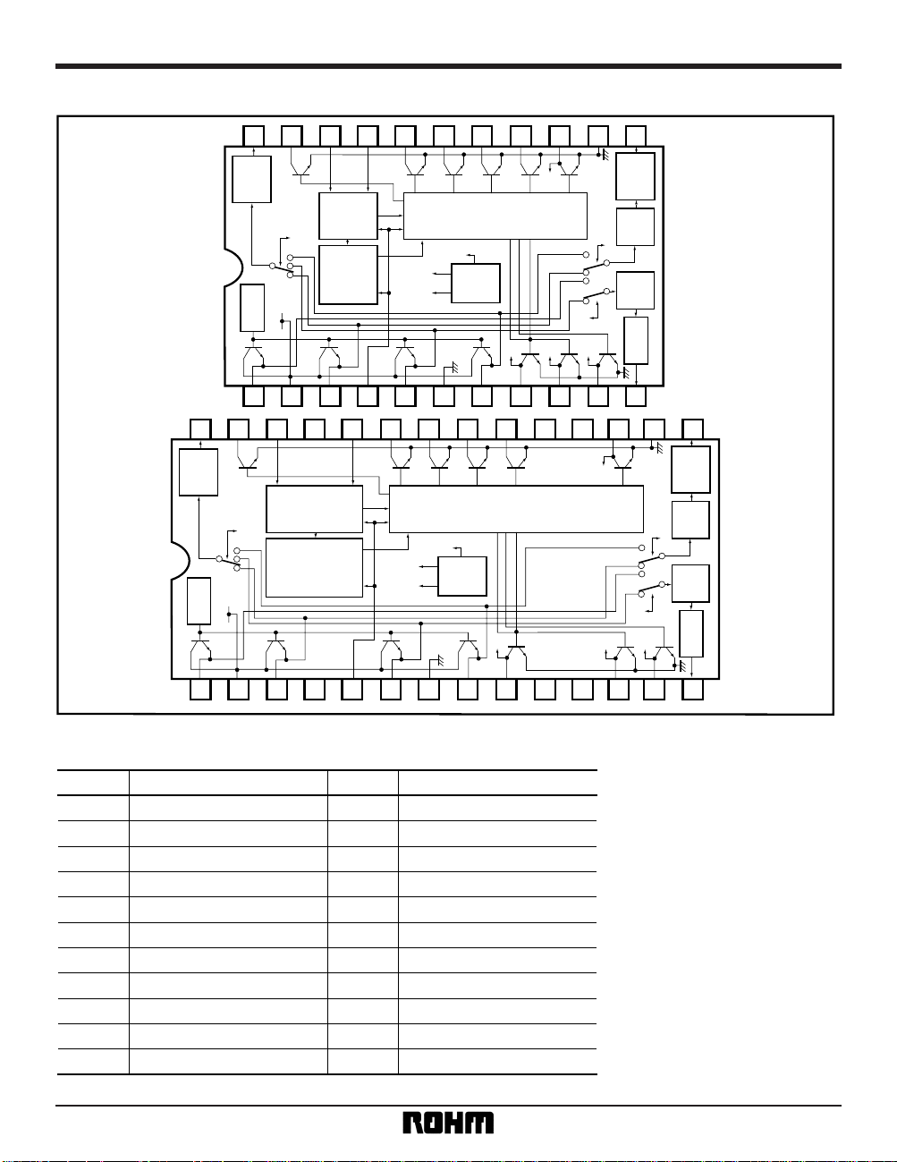
Block diagram
1 2 3 4 5 6 7 8 9 10 11
22 21 20 19 18 17 16 15 14 13 12
BUFF
BIAS
BIAS
BUFF
LOGIC
6dB
AMP
6dB
AMP
CONTROL
LOGIC
LATCHES
SHIFT
REGISTER
SW4
SW3
SW12
SW2
SW1
SW12
SW4
SW3SW2SW1
1 2 3 4 5 6 7 8 9 10 11 12 13 14
17 16 15
28 27 26 25 24 23 22 21 20 19 18
BUFF
BIAS
BUFF
BUFF
LOGIC
6dB
AMP
6dB
AMP
CONTROL
LOGIC
LATCHES
SHIFT
REGISTER
SW4
SW3
SW12
SW2
SW1
SW12
SW4
SW3
SW2
SW1
BA7630S
BA7630F

3
Multimedia ICs BA7630S / BA7630F
•
Electrical characteristics (unless otherwise noted Ta = 25°C and VCC = 5.0V)
Parameter
Symbol Min. Typ. Max. Unit Conditions
Measurement
Circuit
I
CC
——28 40 mA Fig.1
V
om
2.5 2.8 —
V
P-P
f = 1kHz, THD = 0.5%
Fig.1
G
V1
– 0.5 0 0.5 dB f = 1MHz, VIN = 1.0VP-P
GV2
5.5 6.0 6.5 dB f = 1MHz, VIN = 1.0VP-P
Gf
– 4.0 – 1.5 + 1.0 dB
10MHz / 1MHz
V
IN = 1.0VP-P
CTM
—– 60 – 45 dB
f = 4.43MHz
V
IN = 1.0P-P
VTH1 ~ 4
1.0 2.0 3.0 V
V
IH
3.0 —— —
—
V
Fig.3
V
IL
——1.0 V
I
IH
IIL
—
—
—210µA
Fig.2
– 80 – 100 – 150 —µA
I
QH1 ~ 4
150 230 350 µAVCC = 12V
I
QH5 ~ 9
— 050µAVCC = 12V
V
QL
— 0.1 0.5 V ICC = 2mA
Fig.1
f
Max.
250 500 ——kHz
t
su
——0.1 1.0 µs
Supply current
〈Analog〉
Maximum output level
Voltage gain 1
Voltage gain 2
Frequency characteristic
Interchannel crosstalk
〈Digital〉
"H" input voltage
"L" input voltage
"H" input current
"L" input current
"H" output leakage current 1
"H" output leakage current 2
"L" output voltage
Maximum clock frequency
Setup time
SW
1 ~ SW4 switch level

4
Multimedia ICs BA7630S / BA7630F
•
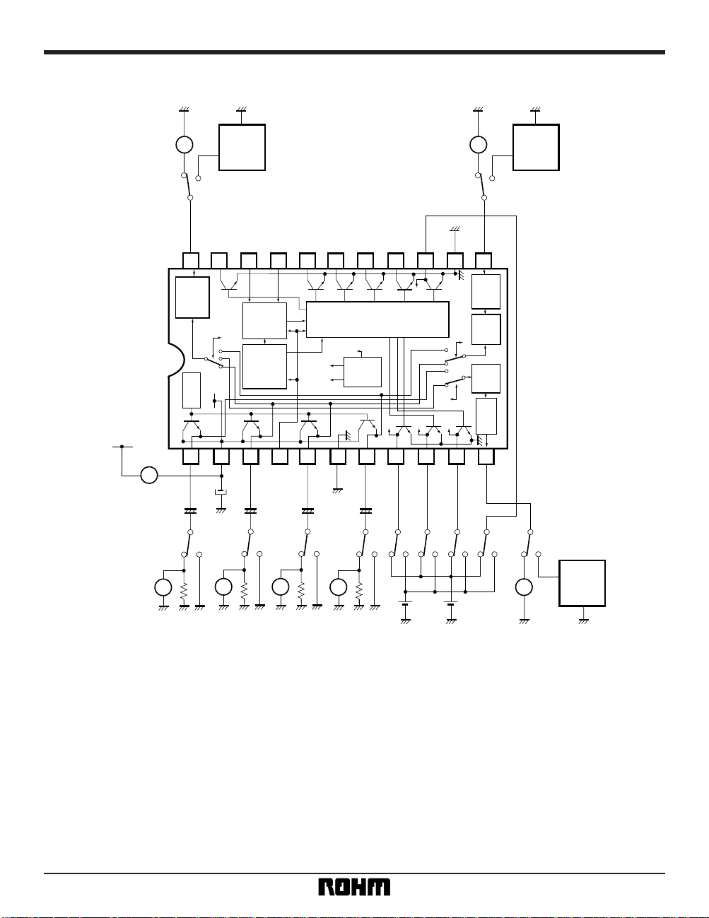
Measurement circuits
BA7630S
22 21
20 1819 17 16 15 14 13
12
1 2
3 54 6 7 8 9 10
11
BUFF
BIAS
BUFF
BUFF
LOGIC
6dB
AMP
6dB
AMP
CONTROL
LOGIC
SHIFT
REGISTER
SW4
SW3
SW12
SW2
SW1
SW12
SW4
SW3SW2SW1
SWD SWE SWF
3V 1V
SW
G SWH SWI
LATCHES
V
21
1111
22222
~
1
50Ω
50Ω
50Ω
50Ω
~
SWC
2
1
~
SWB
2
1
~
SWA
OSC
1µ
47µ
V
CC5.0V
1µ 1µ 1µ
2
1
~
A
SWJ
V
2
1
~
SWK
V
2
1
~
Fig.1
Distortion
meter
Distortion
meter
Distortion
meter
+ + + +
 Loading...