

1
Video ICs
Electronic viewfinder driver
BA7149F
The BA7149F is an electronic viewfinder driver for video cameras. It separates the synchronous signal from the input
video signal, and outputs the vertical deflection drive output and horizontal deflection signals. HD and VD output signals with guaranteed phase difference are also provided for on-screen displays (OSD). The differences between the
BA7149F and the BA7148F are the horizontal blanking, horizontal AFC output, HD output phase and pulse width.
•
Applications
Video cameras
•
Features
1) Operates off a 5V power supply.
2) Built-in vertical deflection circuit.
3) Built-in wide-bandwidth amplifier.
4) Built-in HD and VD output terminals.
5) Few attached components required.
6) SOP 16pin package.
7) Compatible with 10µ sec flyback pulses.
•
Absolute maximum ratings (Ta = 25°C)
Parameter
Symbol Limits Unit
8.0 V
500
∗
mW
°C
°C
V
CC Max.
– 20 ~ + 75
– 55 ~ + 125
Pd
Topr
Tstg
Applied voltage
Power dissipation
Operating temperature
Storage temperature
∗
Reduced by 5mW for each increase in Ta of 1°C over 25°C.
•
Recommended operating conditions (Ta = 25°C)
Parameter
Symbol Min. Typ. Max. Unit
V
CC
4.5 5.0 5.5 V
Power supply voltage
2
Video ICs BA7149F
•
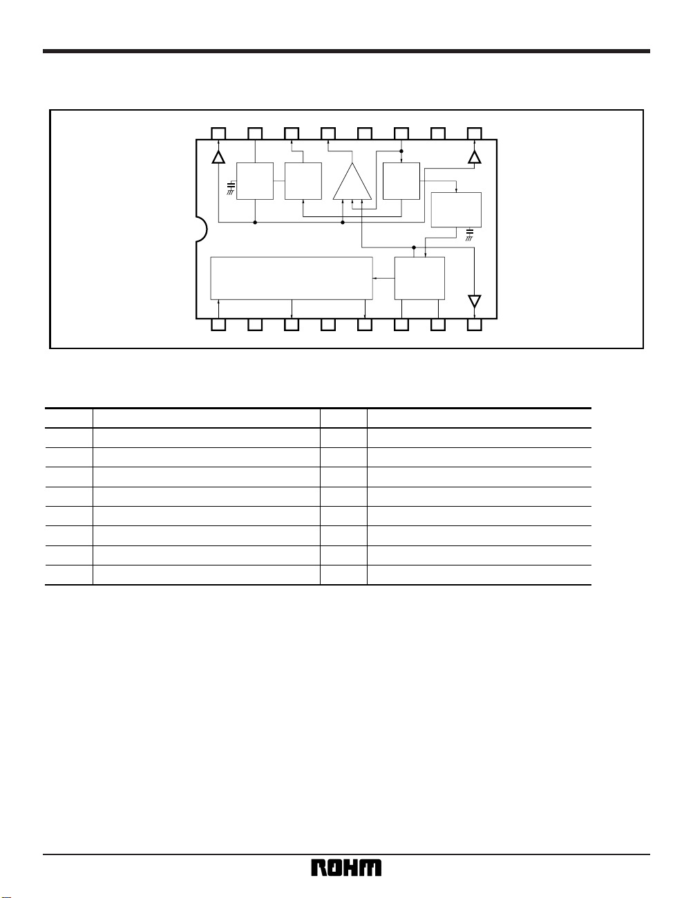
Pin descriptions
FunctionFunction
19
210
311
412
513
614
715
816
Pin No. Pin No.
Vertical control input
Power supply 1
Vertical deflection drive (POS)
GND 1
Vertical deflection drive (NEG)
Vertical oscillator external resistor
Vertical oscillator external capacitor
VD output
HD output
GND 2
Video input
Power supply 2
Video output
Phase comparator output
Horizontal oscillator external resistor
Horizontal AFC output
•
Block diagram
16 15 14 13 12 11 10 9
12345678
H.OSC
PHASE
COMP
6dB
AMP
V.SEPA
V.OSCV.DRIVE
V.BLK
H.BLK
SYNC
SEPA
3
Video ICs BA7149F
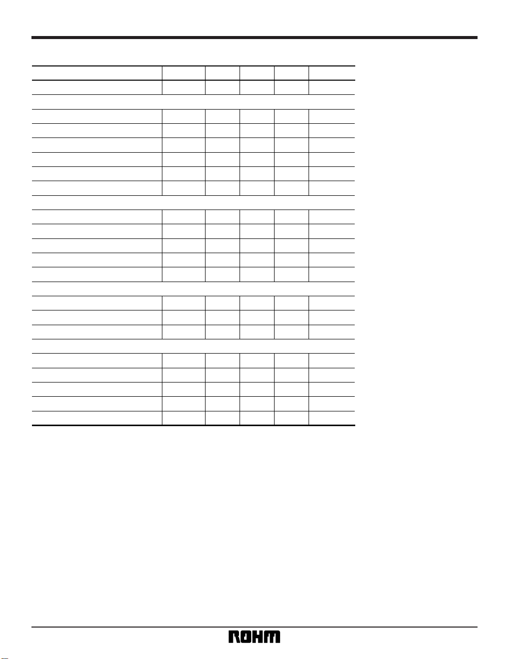
•
Electrical characteristics (unless otherwise noted, Ta = 25°C and Vcc = 5.0V)
Parameter
Symbol Min. Typ. Max. Unit
I
CC
31.0 42.0 55.0 mA
G
V
5.3 6.0 6.7 dB
D
RV
3.20 3.50 —
f
C
– 2.0 0.0 + 2.0 dB
— 45 120
T
H · BL
9.6 10.7 11.4 µs
T
V · BL
870 970 1070 µs
f
H · O
13.9 15.7 17.5
∆f
CAP
± 2.1 ± 3.0 —
T
HP
10.2 11.1 12.0 µs
T
HPH
– 1.9 – 1.2 – 0.5 µs
V
HPL
0.5 1.1 1.7 V
f
V · O
51.3 54.8 58.2 Hz
2.10 2.70 —
2.10 2.70 —
T
HVD
17.3 21.3 25.3 µs
T
HD
8.7 9.9 11.1 µs
T
VD
860 960 1060 µs
V
HV · L
— 0.1 0.3 V
V
HV · H
4.7 4.9 — V
V
P-P
mV
P-P
V
P-P
V
P-P
kHz
kHz
V
syn · Min.
V
VP · Max.
V
VN · Max.
䊊Not designed for radiation resistance.
Operating current dissipation
Voltage gain
D range
Frequency characteristic
Minimum sync separation voltage
Horizontal blanking width
Vertical blanking width
Free-running frequency
Capture range
AFC output pulse width
AFC lock-in phase
Pulse voltage low
Free-running frequency
Pin 3 maximum output amplitude
Pin 5 maximum output amplitude
Phase difference
H
D pulse width
V pulse width
Pulse voltage low
Pulse voltage high
〈VIDEO AMP〉
〈
HD · VD〉
〈
Horizontal〉
〈
Vertical〉

4
Video ICs BA7149F
1pin
V
12pin
1pin
1.9k
10k
500
500
+
2.33V
Fig.1
•
Input / output circuits
2pin
3pin
5pin
4pin
300
300
2, 3, 4, 5pin
Fig.2
6pin
12pin
2k
2k
12k
6pin
1.5V
V
+
Fig.3
8pin
2pin
8pin
10k
20k
20k
Fig.5
9pin
2pin
9pin
25k
10k
20k
Fig.6
7pin
12pin
7pin
12pin
20k 20k
5k 5k 5k
8µA
Fig.4
11pin
11pin
12pin
1k
1.25k
100
100
50
+
1.87V
36µA
V
Fig.8
14pin
12pin
3k
14pin
3k 3k 3k
3k
3k 3k 3k
Fig.9
13pin
12pin
13pin
100
3k
100
1mA
Fig.7

5
Video ICs BA7149F
16pin
2pin
16pin
500
20k
12pin
20k
Fig.11
15pin
12pin
10k
15pin
2k2k
2.8V
10k
10k
12k
V
+
Fig.10
•
Circuit operation
Input signals
63.556µ
H Pulse only
0.29V at 11pin
adj.at 11pin
4.7µ
262.5H
16.683m
V Pulse only
H Pulse only
Pulse IH
Pulse IS
Pulse IV
IH
Fig.12
The video signal input to pin 11 is detected by the charging and discharging of an external capacitor. Sync separation is done in the SYNC SEPA block. The H. SYNC
signal is sent to the H. OSC, and the V. SYNC signal is
sync-separated in the vertical sync pulse interval and supplied to the V. OSC block.
The H. OSC block consists of a PLL that oscillates in sync
with the sync-separated H. SYNC signal, and outputs the
HD pulse and horizontal deflection pulse.
In the V. OSC block, a direct-control method is used with
the sync signal. To synchronize the vertical oscillator cir-
cuit, the inherent oscillation period of the oscillation circuit
is made slightly larger than the vertical sync signal period,
so that the sync signal always enters slightly early.
The oscillator output alone is not enough to ensure stable
operation for the vertical deflection output circuit, so it is
amplified by the V. DRIVE block.
The horizontal and vertical blanking signals generated in
the H. OSC and V. OSC blocks are used to erase the horizontal retrace line from the video signal input to pin 11.
The signal is inverted and amplified by a 6dB inverting
amplifier and output as a negative-polarity video signal.

6
Video ICs BA7149F
•
Application example
FBT
+
16
1
15 14 13 12 11 10 9
8765432
H.OSC
PHASE
COMP
6dB
AMP
SYNC
SEPA
V.SEPA
V.OSCV.DRIVE
V.BLK
H.BLK
+
100k
390k
VIDEO OUT
VIDEO IN
470
+
470
+
0.22
µ
10k
HD
VD
15k
VR1
100
+
3.9
15k
VCC
1µ
1µ
100µ
0.1µ
5mH + 36Ω
0.022µ
47µ
47µ
0.022µ
510k
VCC
1500pF
V
CC
∗
1 The resistors connected to pins 6 and 15 should have a tolerance of ± 2%, and a temperature
coefficient of ± 100ppm or lower.
∗
2 The capacitor connected to pin7 should have a tolerance of ± 5%, and a temperature coefficient of
± 250ppm or lower.
Fig.13

7
Video ICs BA7149F
•
Operation notes
(1) H.OSC free-run frequency and capture range
The free-run frequency is determined by the 115kΩ
resistor connected between pin 15 and GND. The capture range is varied by the resistors and capacitor connected to pins 14 and 15.
The free-run frequency and capture range for this IC
are guaranteed for these circuit constant values, and
we recommend that you use them. The resistor 115kΩ
connected between pin15 and GND should have a tolerance of ± 2%, and a temperature coefficient of ±
100ppm or lower.
(2) V.OSC free-run frequency
The V.OSC free-run frequency is determined by the
15kΩ resistor connected between pin 6 and GND, and
the 0.1µF capacitor connected between pin 7 and
GND.
The free-run frequency and capture range for this IC
are guaranteed for these circuit constant values, and
we recommend that you use them. The resistor 15kΩ
connected between pin 6 and GND should have a tolerance of ± 2%, and a temperature coefficient of ±
100ppm or lower, and the capacitor connected
between pin 7 and GND should have a tolerance of ±
5%, and a temperature coefficient of ± 250ppm or
lower.
(3) Use with PAL systems
In PAL systems, change the value of the resistor connected between pin 6 and GND to 18kΩ.
(4) PCB pattern
The large-signal systems and small-signal systems in
the IC have been kept separate, and the external wring
must also be done in such a way to prevent interference from occurring. In particular, to prevent the FBT
return current from interfering with the V. OSC circuit
on pins 6 and 7, do not directly connect the pin 4 GND
and pin 6 and 7 GND.
1
16
2
3
4
5
6
7
8
9
10
11
12
13
14
15
G
FBT
V
CC
∗
Do not connect pin 4 GND
to pin 6 and 7 GND.
Fig.14
•
External dimensions (Units: mm)
SOP16
0.4 ± 0.11.27
0.15
0.15 ± 0.1
0.3Min.
4.4 ± 0.2
6.2 ± 0.3
0.11
1.5 ± 0.1
1
16
10.0 ± 0.2
8
9
 Loading...