


1
Multimedia ICs
SYNC separator IC with AFC
BA7071F
The BA7071F contains a video synchronization separation circuit, a vertical video synchronization separation circuit,
a horizontal oscillation circuit, and a phase comparator. It separates and outputs the horizontal and vertical synchronization signals (HD and VD), and the composite synchronization signal (Sync-out) from input video or composite
synchronization signals. The phase difference between HD and VD is guaranteed for both the rising and falling
edges of VD.
•
Applications
TVs, VCRs and camcorders
•
Features
1) Built in AFC circuit.
2) HD and VD phase difference guaranteed.
3) Wide supply voltage range (3V to 7V).
4) Horizontal free-run frequency does not require adjustment.
5) Low external parts count.
6) SOP 8-pin package.
•
Recommended operating conditions (Ta = 25°C)
Parameter Symbol Limits Unit
8.0 V
350
∗
mW
Topr °C
°C
V
CC
Tstg
Pd
– 20 ~ + 75
– 55 ~ + 125
Power supply voltage
Power dissipation
Operating temperature
Storage temperature
∗
Reduced by 3.5mW for each increase in Ta of 1°C over 25°C.
Parameter Symbol Min. Typ. Max. Unit
2.85 — 7.5 VV
CCPower supply voltage
•
Absolute maximum ratings (Ta = 25°C)
2
Multimedia ICs BA7071F
•
Pin descriptions
Pin No.
1V
IN
2 HD - OUT
3 GND
4 PD - OUT
5 HOSC - R
6V
CC
7 VD - OUT
8 Sync - OUT
Video input
HD output
GND
Phase comparator output
Horizontal oscillator resistor
Power supply (V
CC)
VD output
Synchronization signal output
FunctionPin name
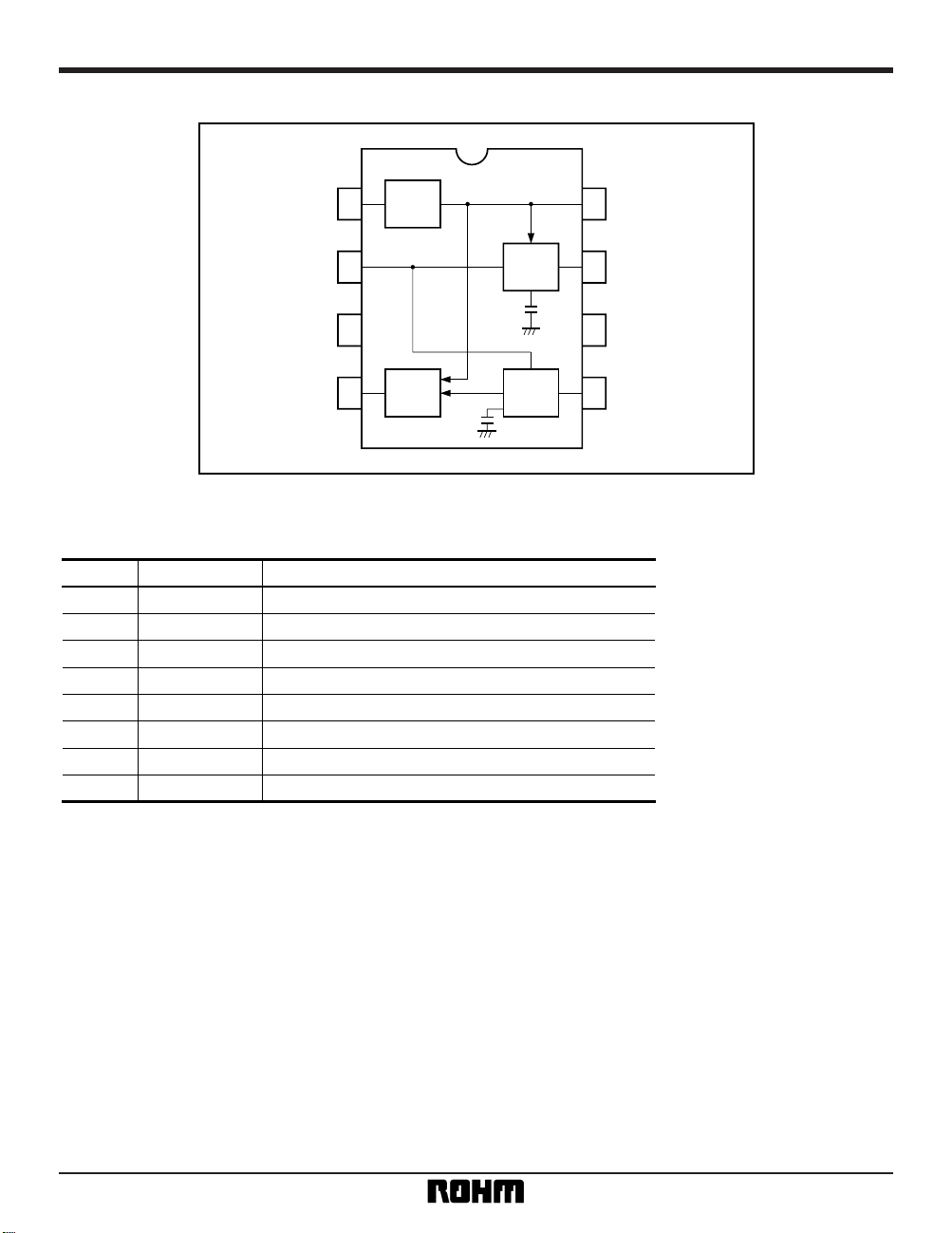
•
Block diagram
1
2
3
45
6
7
8
Vsepa
VCO
VIN
HD - OUT
GND
PD - OUT
Sync - OUT
VD - OUT
V
CC
HOSC - R
SYNC
SEPA
PD
COMP

3
Multimedia ICs BA7071F
5pin
1pin
2pin
4pin
VCC
VCC
VCC
VIN HOSC - R HD - OUT
VCC
VD - OUT PD - OUT Sync - OUT
8pin
V
CCVCC
7pin
•
Input / output circuits
•
Electrical characteristics (unless otherwise noted Ta = 25°C and VCC = 5.0V)
pin 2 pin – 1
pin 7 pin – 2 (FLD1)
pin 7 pin – 2 (FLD1)
pin 2
pin 7
pin 1 pin – 7
Parameter Symbol Min. Typ. Max. Unit Conditions
3.0 5.8 8.6 mA
0.08 0.15
V
p
-L ——0.1 0.3
Vsyn-min
Vp-H
f
H.O
T
HPH
T
HVD1
T
HVD2
T
HD
T
VD
T
INVD
I
Q
∆f
CAP
4.7
13.5
2.3
0.6
19.0
19.0
9.0
249
41.0
5.0
15.7
2.7
1.6
24.0
24.0
10.0
254
48.0
—
17.9
——
2.6
29.0
29.0
11.0
259
55.0
V
V
kHz
kHz
µs
µs
µs
µs
µs
µs
V
P-P
pins 2, 7
pins 2, 7
pin 8 open
pin 1 terminated with 75Ω
resistor
No input signal
Quiescent current
Minimum SYNC separation level
Pulse voltage low
Pulse voltage high
Capture range
Lock-in phase
HD, VD phase deviation 1
HD, VD phase deviation 2
HD pulse width
VD pulse width
V
IN
, VD phase difference
(Horizontal)
free-running frequency

4
Multimedia ICs BA7071F
1
2
3
45
6
7
8
Vsepa
VCO
+
0.47µF 0.022µF
+
+
0.47µ
1µF
C1
C3
R2
220kΩ
100kΩR1
C4 C5
R4
PD
COMP
SYNC
SEPA
2200pF
VIDEO IN
HD OUT
SYNC OUT
V
CC
VD OUT
VCC = 5V, 18kΩ
VCC = 3V, 10kΩ
R3
VCC
20kΩ
VCC
+
0.47µ
•
Measurement circuit (application example)
(1) Connect a 100kΩ resistor between pin 5 and ground.
Leave pins 2, 4 and 7 open.
(2) SYNC OUT (pin 8) has positive output.
(3) The SYNC OUT (pin 8) output rise delay times in relation to the VIDEO IN (pin 1)
input signal Sync fall are as follws:
830 ns (reference value) ,when V
CC = 5V
880 ns (reference value) ,when V
CC = 3V
(4) The SYNC OUT (pin 8) output fall delay times in relation to the VIDEO IN (pin 1)
input signal Sync rise are as follws:
150 ns (reference value) ,when V
CC = 5V
220 ns (reference value) ,when V
CC = 3V
1
2
3
45
6
7
8
Vsepa
VCO
+
0.47µF 0.022µF
+
1µF
C1
100kΩR1
C4 C5
R4
PD
COMP
SYNC
SEPA
VIDEO IN
SYNC OUT
V
CC
VCC
20kΩ
Fig. 1
When SYNC SEPA output only is used. HD and VD unused.

5
Multimedia ICs BA7071F
•
Circuit operation
(1) Synchronization separation circuit
Detects the charging current to a externally-connected
capacitor, and performs synchronization separation.
(2) Horizontal oscillation circuit
When a video signal is input, it is synchronized with
Hsync by the PLL. The horizontal free-running frequency is determined by external resistor R
1.
(3) Vertical synchronization separation circuit
When a video signal is input, synchronization signal
separation is done over the vertical synchronization
pulse interval.
f
H • O = [kHz]
1.57E6
R
1
(4) VIN, HD, and VD timing charts
1 / 2H
V
D
(OUT)
VIN, VD phase difference
Vertical synchronization pulse interval
NTSC signal
Odd field (IN)
NTSC signal
Even field (IN)
H
D
Odd field (OUT)
H
D
Even field (OUT)
1. The rise and fall positions for VD are basically the same for both odd and even fields.
2. H
D shifts by 1 / 2H during the odd and even field interval.
3. Only the odd field is given for the specification.
HD, VD phase difference 1
Fig. 2
HD, VD phase difference 2
•
Attached components
Resistor R
1 should have a tolerance of ± 2%, and a
temperature coefficient of 100ppm or lower.

6
Multimedia ICs BA7071F
•
Electrical characteristic curves
0
– 25
2
4
6
8
10
0 255075
TEMPERATURE : Ta (°C)
V
CC = 5.0V
QUIESCENT CURRENT : IQ (mA)
Fig. 3 Quiescent current vs.
temperature
0
– 250 255075
0
250
200
150
100
50
TEMPERATURE : Ta (°C)
MINIMUM SYNC - SEPA LEVEL : Vsyn - Min. (VPP)
VCC = 5.0V
Fig. 4 Minimum synchronization
separation level vs.
temperature
– 250 255075
16.2
16.0
15.8
15.6
15.4
15.2
TEMPERATURE : Ta (°C)
HORIZONTAL FREQUENCY : fH.O (kHz)
VCC = 5.0V
Fig. 5 Horizontal free-running
frequency vs.
temperature
– 250 255075
10.4
10.2
10.0
9.8
9.6
TEMPERATURE : Ta (°C)
NTSC
9.4
HD PULSE WIDTH : THD (µs)
VCC = 5.0V
Fig. 6 HD pulse width vs.
temperature
230
– 250 255075
280
270
260
250
240
TEMPERATURE : T (°C)
VD PULSE WIDTH : TVD (µs)
NTSC
V
CC = 5.0V
Fig. 7 VD pulse width vs.
temperature
– 250 255075
00
30
28
26
24
22
20
TEMPERATURE : Ta (°C)
HD · VD PULSE TIMING 1 : THDV1 (µs)
NTSC
V
CC = 5.0V
Fig. 8 HD, VD phase difference 1 vs.
temperature
– 250 255075
00
30
28
26
24
22
20
TEMPERATURE : Ta (°C)
NTSC
HD · VD PULSE TIMING 2 : THDV2 (µs)
VCC = 5.0V
Fig. 9 HD, VD phase difference 2 vs.
temperature

7
Multimedia ICs BA7071F
SOP8
0.4 ± 0.11.27
0.15
0.3Min.
0.15 ± 0.1
0.11
6.2 ± 0.3
4.4 ± 0.2
5.0 ± 0.2
85
41
1.5 ± 0.1
•
External dimensions (Units: mm)
 Loading...