ROHM BA7046F, BA7046 Datasheet

1
Multimedia ICs
SYNC separator IC with AFC
BA7046 / BA7046F
The BA7046 and BA7046F separate the synchronization signals from a video signal and output the horizontal and
vertical synchronization signals (H
D and VD), and the composite synchronization signal (Sync-out).
The H
D and VD pulse phase difference is guaranteed.
•
Applications
TVs and VCRs
•
Features
1) Built-in AFC circuit.
2) H
D and VD phase difference guaranteed.
3) Low power dissipation. (approx. 21mW)
4) Low external parts count.
5) 8-pin DIP / SOP package.
6) Horizontal free-run frequency does not require
adjustment.
•
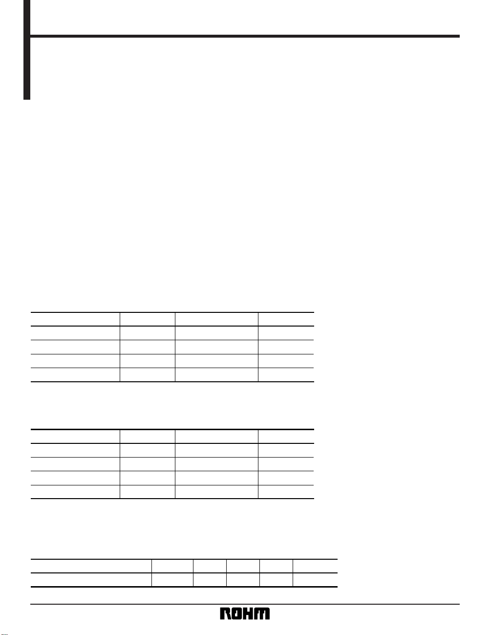
Absolute maximum ratings (Ta = 25°C)
BA7046 (DIP)
BA7046F (SOP)
•
Recommended operating conditions (Ta = 25°C)
Parameter Symbol Unit
V
CC Max. 8.0 V
500
∗
mV
Topr °C
Tstg °C
Pd
Limits
– 20 ~ + 75
– 55 ~ + 125
Power supply voltage
Power dissipation
Operating temperature
Storage temperature
∗
Reduced by 5mW for each increase in Ta of 1°C over 25°C.
Parameter Symbol Unit
8.0 V
350
∗
mW
Topr °C
Tstg °C
Pd
V
CC Max.
Limits
– 20 ~ + 75
– 55 ~ + 125
Power supply voltage
Power dissipation
Operating temperature
Storage temperature
∗
When mounted on a 50mm × 50mm PCB board, reduced by 3.5mW for each increase in Ta of 1°C
over 25°C.
Parameter Symbol Min. Typ. Max. Unit
V
CC 4.5 — 5.5 VOperating power supply voltage

2
Multimedia ICs BA7046 / BA7046F
•
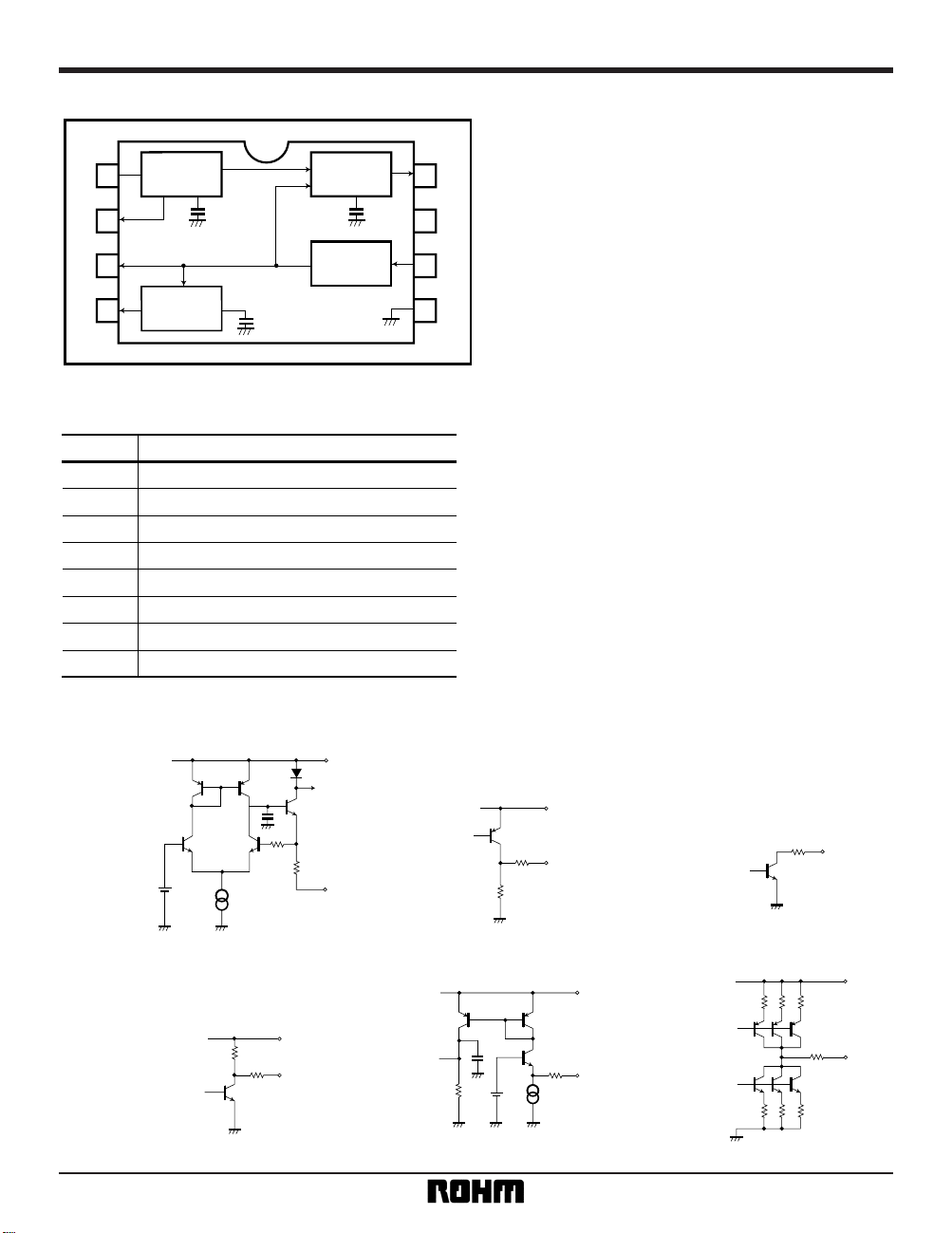
Input / output circuits
VCC
1pin
1k
12k
100µA
Fig. 1
200
VCC
10k
4pin
Fig. 4
VCC
100
6pin
10µA
Fig. 5
8pin
V
CC
3k3k3k
3k3k3k
1k
Fig. 6
5k
VCC
2pin
200
Fig. 2
3pin
200
Fig. 3
•
Block diagrams
•
Pin descriptions
1
2
3
4
8
7
6
5
H. OSC
V. SEPA
PHASE
COMP
SYNC
SEPA
1
2
3
4
5
6
7
8
Pin No.
Horizontal oscillator resistor
H
D output
SYNC output (open collector)
V
D output
GND
Video input
Power supply
Phase comparator output
Function

3
Multimedia ICs BA7046 / BA7046F
•
Electrical characteristics (unless otherwise noted Ta = 25°C and VCC = 5.0V)
Parameter Symbol Min. Typ. Max. Unit Conditions
I
Q
2.0 4.1 6.2 mA
—
0.08 0.15
—
0.1 0.3 V
4.7 4.9
—
V
13.9 15.7 17.5 kHz
±
2.1± 2.9
—
kHz
T
HPH
–
1.0 0
+
1.0µs pin2 pin– 6
T
HVD
17.0 23.5 30.0µs pin4 pin– 2
T
HD
4.6 5.1 5.6µs
pin2
TVD190 230 270µs pin4
V
syn-Min.
V
P-L
V
P-H
f
H-O
V
P-P
∆
f
CAP
pins 2, 4
䊊
Not designed for radiation resistance.
Quiescent current
Minimum synchronization separation level
Pulse voltage, LOW
Pulse voltage, HIGH
(Horizontal) free-running frequency
Capture range
Lock-in phase difference
H
D
, VD phase difference
H
D
pulse width
V
D
pulse width
pin 3 open
pin 6 terminated with 75
Ω
resistor
pins 2, 4
No input signal, I
1
=
open
•
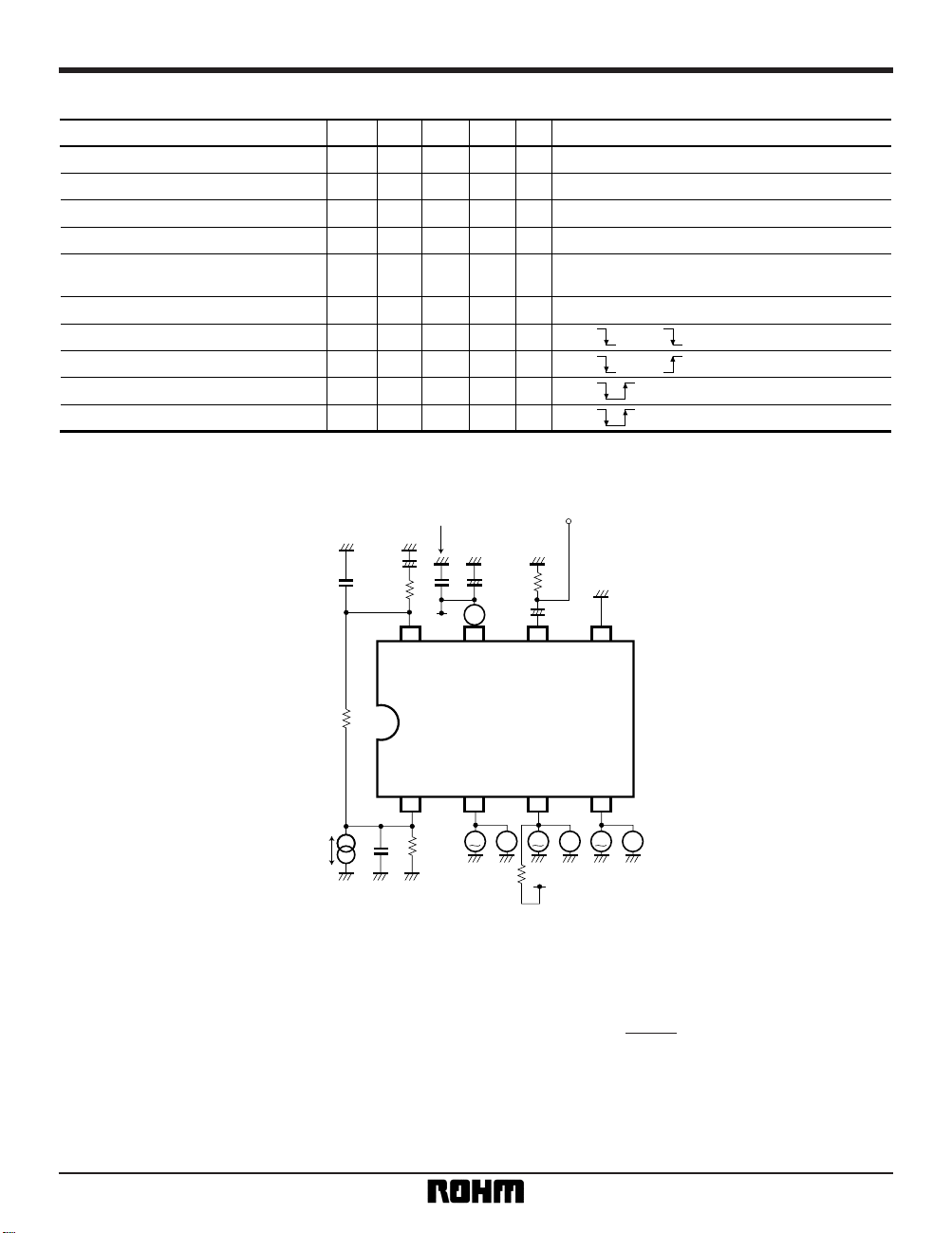
Measurement circuit
8 7 6 5
1 2 3 4
II
100p
130k
V
T
V
T
V
T
1µ
1µ
75
Video In
+
+
+
A
47µ
0.022µ
39k
VCC
2200p
470k
10k V
CC
Fig. 7
•
Circuit operation
(1) Synchronization separation circuit
Detects the charging current to a externally-connected
capacitor, and performs synchronization separation.
(2) Horizontal oscillation circuit
When a video signal is input, it is synchronized with
Hsync by the PLL. The horizontal free-running frequency
is determined by external resistor R1.
(3) Vertical synchronization separation circuit
When a video signal is input, synchronization signal
separation is done over the vertical synchronization
pulse interval.
f
H-O = [kHz]
2.05E6
R
1
 Loading...