

1/3
STRUCTURE Silicon Monolithic Integrated Circuit
PRODUCT SERIES 2-Phase Half-Wave Motor Driver for Fan Motor
TYPE
BD6701F
FEATURES Built - in reverse current protection diode
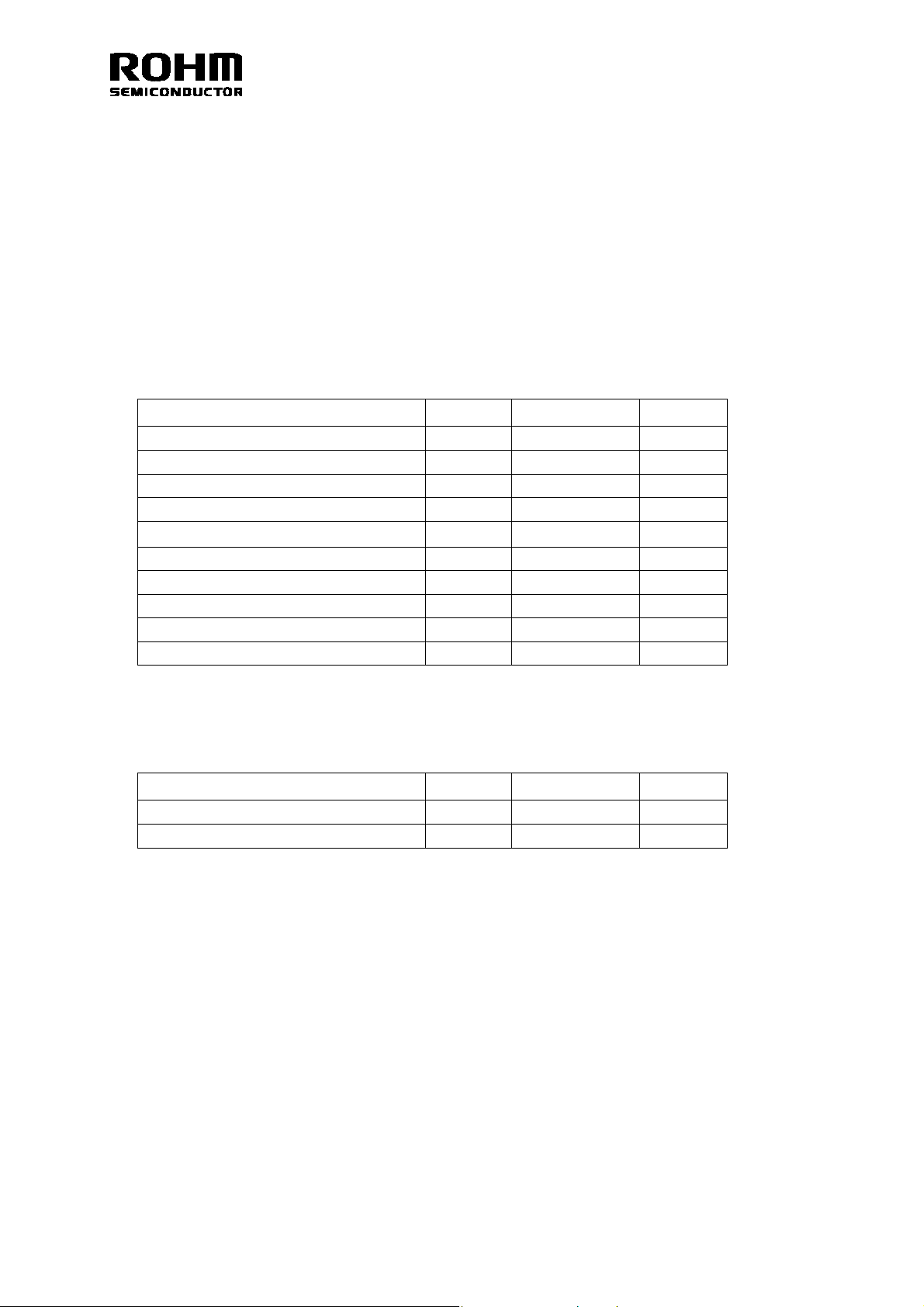
〇ABSOLUTE MAXIMUM RA TINGS
Parameter
Supply voltage
Power dissipation
Operating temperature range
Storage temp erature range
Output current
AL signal output current
AL signal output voltage
FG signal output current
FG signal output voltage
Junction temperature
Symbol Limit Unit
Vcc 36 V
Pd 780* mW
Topr -40~+100 ℃
Tstg -55~+150 ℃
Iomax 800** mA
IAL 10 mA
VAL 36 V
IFG 10 mA
VFG 36 V
Tjmax 150 ℃
* To use at temperature abov e Ta=25℃ reduce 6.24mW/℃.
(On 70.0mm×70.0mm×1.6mm glass epoxy board)
** This value is not to be over Pd.
〇OPERATING CONDITIONS
Parameter
Operating supply voltage range
Hall input voltage range
*This product is not designed for production against radioactive rays.
Symbol
Limit Unit
Vcc 6.0~28.0 V
VH 0~Vcc-3.0 V
REV. C
2/3
1
A
〇ELECTRICAL CHARACTERISTICS (Unless otherwise specified Ta=25℃,Vcc=12V)
Parameter
Circuit current
Hall input offset voltage
Hall input hysteresis
Output L voltage
Output leak current
Output zenner voltage
Lock detection ON time
Lock detection OFF time
AL terminal voltage L
AL terminal leak current
FG terminal voltage L
FG terminal leak current
Symbol
Min. Typ. Max.
Icc 3 6 9 mA
VHofs -10 - 10 mV
Vhys ±5 ±10 ±15 mV
VOL - 0.30 0.50 V Io=200mA
IOL - - 100 μA Vo=45V
VOZ 50 54 58 V Clamp current=10mA
TON 0.30 0.50 0.70 sec
TOFF 3.0 5.0 7.0 sec
VALL - - 0.4 V IAL=5mA
IALL - - 50 μA VAL=36V
VFGL - - 0.4 V IFG=5mA
IFGL - - 50 μA VFG=36V
Limit
Unit Conditions
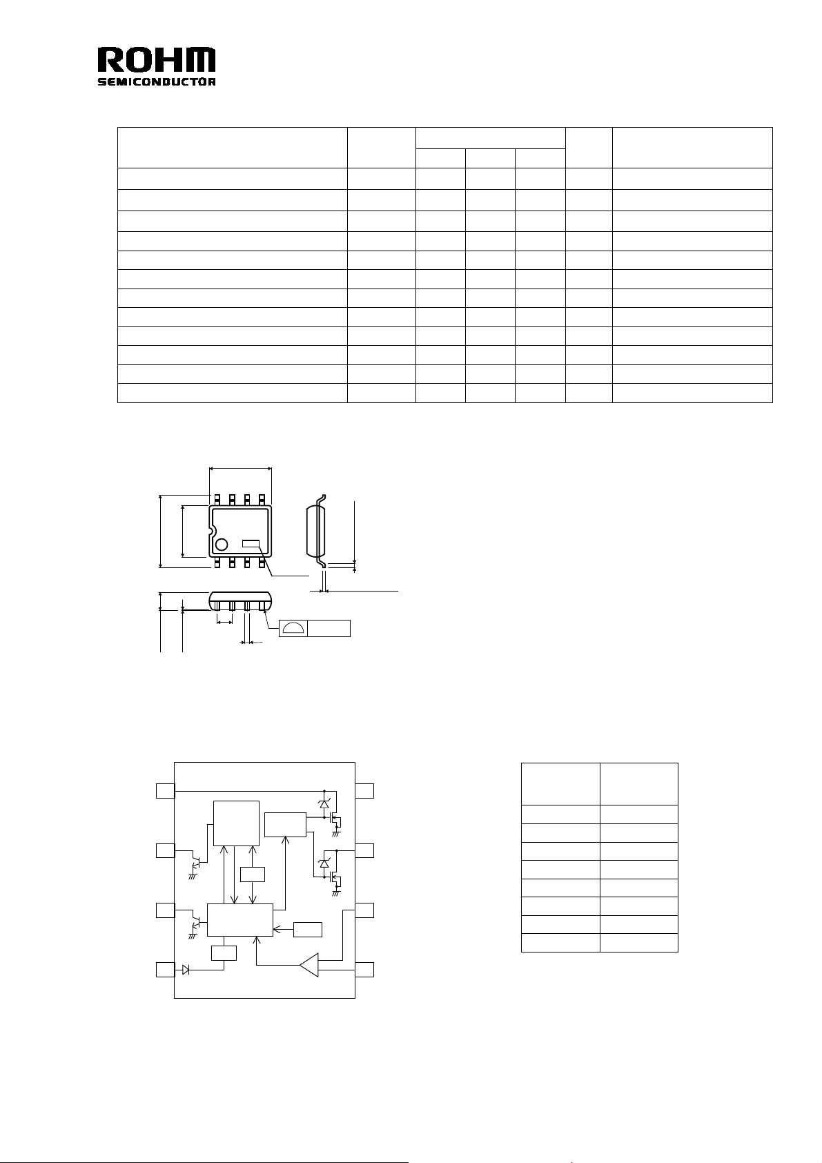
〇P ACKAGE OUTLINES
5.0±0.2
6.2±0.3
85
6701
4.4±0.2
41
0.3Min.
Lot No.
0.15±0.1
1.27
0.11
1.5±0.1
0.4±0.1
0.1
SOP 8(UNIT:mm)
〇BLOCK DIAGRAM 〇Terminal name
OUT2
L
2
FG
3
Vcc
4
Detect
Restart
REG
Lock
Auto
OSC
Control
Pre Drive
HALL
AMP
TSD
-
+
GND
8
OUT1
7
H-
6
H+
5
Pin No.
1 OUT2
2 AL
3 FG
4 Vcc
5 H+
6 H7 OUT1
8 GND
Terminal
name
REV. C

3/3
〇CAUTIONS ON USE
1) Absolute maximum ratings
An excess in the absolute maximum rations, such as supply voltage, temperature range of operating conditions, etc., can break down
the devices, thus making impossible to identify breaking mode, such as a short circuit or an open circuit. If any over rated values will
expect to exceed the absolute maximum ratings, consider adding circuit protection devices, such as fuses.
2) Connecting the power supply connector backward
Connecting of the power supply in reverse polarity can damage IC. Take precautions when connecting the power supply lines. An
external direction diode can be added.
3) Power supply line
Back electromotive force causes regenerated current to power supply line, therefore take a measure such as placing a capacitor
between power supply and GND for routing regenerated current. And fully ensure that the capacitor characteristics have no problem
before determine a capacitor value. (when applying electrolytic capacitors, capacitance characteristic values are reduced at low
temperatures)
4) GND potential
The potential of GND pin must be minimum potential in all operating conditions. Also ensure that all terminals except GND terminal
do not fall below GND voltage including transient characteristics. However, it is possible that the motor output terminal may deflect
below GND because of influence by back electromotive force of motor. Malfunction may possibly occur depending on use condition,
environment, and property of individual motor. Please make fully confirmation that no problem is found on operation of IC.
5) Thermal design
Use a thermal design that allows for a sufficient margin in light of the power dissipation(Pd) in actual operating conditions.
6) Inter-pin shorts and mounting errors
Use caution when positioning the IC for mounting on printed circuit boards. The IC may be damaged if there is any connection error
or if pins are shorted together.
7) Actions in strong electromagnetic field
Use caution when using the IC in the presence of a strong electromagnetic field as doing so may cause the IC to malfunction.
8) ASO
When using the IC, set the output transistor so that it does not exceed absolute maximum rations or ASO.
9) Thermal shut down circuit
The IC incorporates a built-in thermal shutdown circuit (TSD circuit). Operation temperature is 175℃(typ.) and has a hysteresis width
of 25℃(typ.). When IC chip temperature rises and TSD circuit works, the output terminal becomes an open state. TSD circuit is
designed only to shut the IC off to prevent thermal runaway. It is not designed to protect the IC or guarantee its operation. Do not
continue to use the IC after operation this circuit or use the IC in an environment where the operation of this circuit is assumed.
10) Testing on application boards
When testing the IC on an application board, connecting a capacitor to a pin with low impedance subjects the IC to stress. Always
discharge capacitors after each process or step. Always turn the IC’s power supply off before connecting it to or removing it from a jig
or fixture during the inspection process. Ground the IC during assembly steps as an antistatic measure. Use similar precaution when
transporting or storing the IC.
11) GND wiring pattern
When using both small signal and large current GND patterns, it is recommended to isolate the two ground patterns, placing a single
ground point at the ground potential of application so that the pattern wiring resistance and voltage variations caused by large
currents do not cause variations in the small signal ground voltage. Be careful not to change the GND wiring pattern of any external
components, either.
12) Capacitor between output and GND
When a large capacitor is connected between output and GND, if Vcc is shorted with 0V or GND for some cause, it is possible that
the current char
below 100uF.
13) IC terminal input
When Vcc voltage is not applied to IC, do not apply voltage to each input terminal. When voltage above Vcc or below GND is applied
to the input terminal, parasitic element is actuated due to the structure of IC. Operation of parasitic element causes mutual
interference between circuits, resulting in malfunction as well as destruction in the last. Do not use in a manner where parasitic
element is actuated.
ged in the capacitor may flow into the output resulting in destruction. Keep the capacitor between output and GND
REV. C

Notes
No copying or reproduction of this document, in par t or in whole, is permitted without the
consent of ROHM Co.,Ltd.
The content specied herein is subject to change for improvement without notice.
The content specied herein is for the purpose of introducing ROHM's products (hereinafter
"Products"). If you wish to use any such Product, please be sure to refer to the specications,
which can be obtained from ROHM upon request.
Examples of application circuits, circuit constants and any other information contained herein
illustrate the standard usage and operations of the Products. The peripheral conditions must
be taken into account when designing circuits for mass production.
Great care was taken in ensuring the accuracy of the information specied in this document.
However, should you incur any damage arising from any inaccuracy or misprint of such
information, ROHM shall bear no responsibility for such damage.
The technical information specied herein is intended only to show the typical functions of and
examples of application circuits for the Products. ROHM does not grant you, explicitly or
implicitly, any license to use or exercise intellectual property or other rights held by ROHM and
other parties. ROHM shall bear no responsibility whatsoever for any dispute arising from the
use of such technical information.
The Products specied in this document are intended to be used with general-use electronic
equipment or devices (such as audio visual equipment, ofce-automation equipment, communication devices, electronic appliances and amusement devices).
The Products specied in this document are not designed to be radiation tolerant.
While ROHM always makes efforts to enhance the quality and reliability of its Products, a
Product may fail or malfunction for a variety of reasons.
Please be sure to implement in your equipment using the Products safety measures to guard
against the possibility of physical injury, re or any other damage caused in the event of the
failure of any Product, such as derating, redundancy, re control and fail-safe designs. ROHM
shall bear no responsibility whatsoever for your use of any Product outside of the prescribed
scope or not in accordance with the instruction manual.
The Products are not designed or manufactured to be used with any equipment, device or
system which requires an extremely high level of reliability the failure or malfunction of which
may result in a direct threat to human life or create a risk of human injury (such as a medical
instrument, transportation equipment, aerospace machinery, nuclear-reactor controller, fuelcontroller or other safety device). ROHM shall bear no responsibility in any way for use of any
of the Products for the above special purposes. If a Product is intended to be used for any
such special purpose, please contact a ROHM sales representative before purchasing.
If you intend to export or ship overseas any Product or technology specied herein that may
be controlled under the Foreign Exchange and the Foreign Trade Law, you will be required to
obtain a license or permit under the Law.
Notice
www.rohm.com
© 2011 ROHM Co., Ltd. All rights reserved.
Thank you for your accessing to ROHM product informations.
More detail product informations and catalogs are available, please contact us.
ROHM Customer Support System
http://www.rohm.com/contact/
R1120
A
 Loading...