

1
Memory ICs
Reset IC with battery backup function
BA6129AF / BA6162 / BA6162F
The BA6129AF, BA6162, and BA6162F are reset ICs with a battery backup function, designed for equipment using
SRAMs and other similar components. These ICs are configured of a reset signal and CS signal output unit and a
power supply switching unit. If the BA6129AF detects that the power supply has dropped to 3.5V or lower, it outputs
the CS, CSB, and Reset signals to set the SRAM in backup mode. If the voltage drops to 3.3V or lower, the power
supply switches to the battery. With the BA6162 and BA6162F, in the same way, a power supply of 4.2V is detected,
and if the voltage drops to 3.3V or lower, the power supply switches to the battery. These ICs allow SRAMs to be
write protected and allow the system to be reset, in addition to switching between the power supply and the battery.
•
Applications
Equipment using SRAMs (cards, cassettes, facsimile machines, copiers, word processors, personal computers, etc.)
•
Features
1) Equipped with battery backup function.
2) Equipped with both CS signals (CS and CSB) and
Reset signals.
3) Low current dissipation when powered from battery.
4) Low voltage loss when powered from battery.
5) Smooth switching between power supply and battery.
•
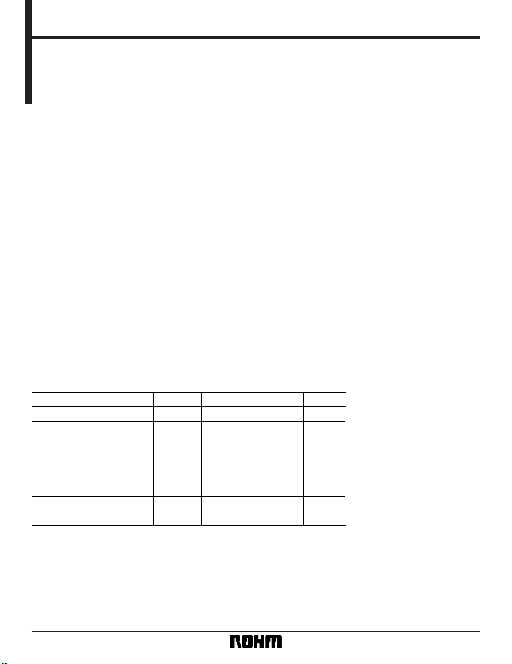
Absolute maximum ratings (Ta = 25°C)
IOUT1 indicates the output current on the VCC side, and IOUT2 the output current on the VBAT side.
Parameter Symbol Limits Unit
Power supply voltage V
CC 7.0 V
Output current 1
I
OUT1
– 80 (BA6129AF)
mA
Output current 2 I
OUT2 – 200 µ
A
Power dissipation
900
∗
1
(BA6162)
550
∗
2
(BA6129AF)
(BA6162F)
mW
Operating temperature – 20 ~ + 75 °C
Storage temperature – 40 ~ + 125 °C
Topr
Pd
Tstg
∗
1 Reduced by 9.0mW for each increase in Ta of 1°C over 25°C.
∗
2 Reduced by 5.5mW for each increase in Ta of 1°C over 25°C.
– 40 (BA6162 / BA6162F)
+
–
+
–
+
–
8765
4321
N.C. Vo CSB
CSResetGND
V
REF
V
BAT
VCC
2
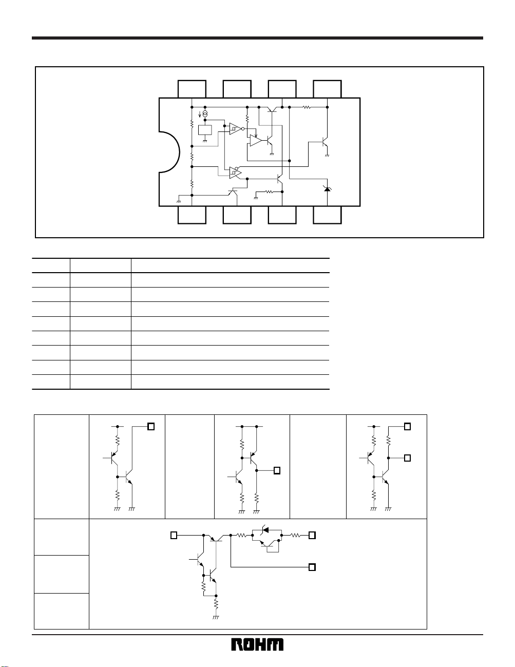
Memory ICs BA6129AF / BA6162 / BA6162F
•
Input / output circuit
Pin 2
Reset
output
Pin 3
CS output
Pin 5
CSB output
Pin 6
Power supply
output
Pin 4
Battery
power supply
Pin 8
Power supply
(V
CC)
Pin 6
Power supply
output
GND
2 6
GND
5
GND
GND
8
4
6
3
VCC VCC VCC
•
Pin descriptions
Pin name Function
1 GND Substrate GND
2 Reset Reset output
3CSCS output
4 Battery power supply
5 CSB CSB output
6V
O Power supply output
7
8 Power supply voltage
V
BAT
VCC
Pin No.
N.C.
—
•
Block diagram

3
Memory ICs BA6129AF / BA6162 / BA6162F
Parameter Symbol Min. Typ. Max. Unit Conditions
I
CC
——
2.0 mA VCC =
5V, V
BAT
=
3V
V
SAT1
—
0.03 0.05 V VCC =
5V, V
BAT
=
3V, IO = –
1mA
V
O1
4.95 4.97
—
VVCC =
5V, V
BAT
=
3V, IO = –
1mA
V
O2
4.70 4.90
—
VVCC =
5V, V
BAT
=
3V, IO = –
15mA
V
O3
4.50 4.86
—
VVCC =
5V, V
BAT
=
3V, IO = –
30mA
V
S
3.35 3.50 3.65 V VCC = H→
L
V
SH
—
100
—
mV VCC = L→
H
V
RESL
——
0.4 V VCC =
3V
I
RESH
——
0.1
µ
A
V
OPL
—
0.8 1.2 V VCC = H→
L, V
RES
⬉
0.4V
V
CSL
——
0.1 V VCC =
3V, V
BAT
=
3V, ICS = + 1µ
A
V
CSH
4.9
——
VVCC =
5V, V
BAT
=
3V, ICS = – 1µ
A
V
CSBL
——
0.1 V VCC =
5V, V
BAT
=
3V, I
CSB
= + 1µ
A
V
CSBH
Vo
–
0.1
——
VVCC =
3V, V
BAT
=
3V, I
CSB
= – 1µ
A
—
—
VS–
0.05
—
+ 0.05 %
/
°C
V
B
3.15 3.30 3.45 V VCC = H→
L, V
BAT
=
3V, RO =
200k
Ω
V
BH
—
100
—
mV VCC = L→
H, V
BAT
=
3V, RO =
200k
Ω
VB–
0.05
—
+ 0.05 %
/
°C
I
CCB
——
0.5
µ
AVCC =
GND, V
BAT
=
3V
V
SAT2
—
0.20 0.30 V VCC =
GND, V
BAT
=
3V, IO = – 1µA
V
O4
2.70 2.80
—
VVCC =
GND, V
BAT
=
3V, IO = – 1µ
A
V
O5
2.60 2.67
—
VVCC =
GND, V
BAT
=
3V, IO = –
100µA
I
OR
——
0.1
µ
AVCC =
5V, V
BAT
=
GND
V
CC
=
5V, VR
RES
=
7V
(Note) IO, ICS, and I
CSB
are
+
when flowing toward the pin and
–
when flowing away from the pin.
䊊
Not designed for radiation resistance.
VO6VCC – 0.5
——
V IO = –
80mA
No-load current
dissipation
I / O voltage differential 1
Vo output voltage 1
Vo output voltage 2
Vo output voltage 3
Detection voltage
Detection hysteresis voltage
Reset output
low level
voltage
Reset leakage current
Reset operating limit voltage
CS output
low level
voltage
CS output
high level
voltage
CSB output
low level
voltage
CSB output
high level
voltage
Detection voltage temperature characteristic
Switching voltage
Switching hysteresis voltage
Switching voltage temperature characteristic
Backup current
dissipation
I / O voltage differential 2
Vo output voltage 4
Vo output voltage 5
Vo output voltage 6
Reverse current
•
Electrical characteristics
BA6129AF (unless otherwise noted, Ta = 25°C, VR
RES = VCC = 5V, RRES = 10kΩ)

4
Memory ICs BA6129AF / BA6162 / BA6162F
Parameter Symbol Min. Typ. Max. Unit Conditions
I
CC
——
2.0 mA V
CC = 5V, VBAT = 3V
V
SAT1
—
0.03 0.05 V V
CC = 5V, VBAT = 3V, IO = – 1mA
V
O1 4.95 4.97
—
VVCC = 5V, VBAT = 3V, IO = – 1mA
V
O2 4.70 4.90
—
VVCC = 5V, VBAT = 3V, IO = – 15mA
V
O3 4.50 4.86
—
VVCC = 5V, VBAT = 3V, IO = – 30mA
V
S 4.00 4.20 4.40 V VCC = H→
L
V
SH
—
100
—
mV V
CC = L→
H
V
RESL
——
0.4 V V
CC = 3.7V
I
RESH
——
0.1 µ
A
V
OPL
—
0.8 1.2 V V
CC = H→
L, V
RES ⬉
0.4V
V
CSL
——
0.1 V V
CC = 3.7V, VBAT = 3V, ICS = + 1µ
A
V
CSH 4.9
——
VVCC = 5V, VBAT = 3V, ICS = – 1µ
A
V
CSBL
——
0.1 V V
CC = 5V, VBAT = 3V, ICSB = + 1µ
A
V
CC = 5V, VRRES = 7V
No-load current dissipation
I / O voltage differential 1
Vo output voltage 1
Vo output voltage 2
Vo output voltage 3
Detection voltage
Detection hysteresis voltage
Reset output low level voltage
Reset leakage current
Reset operating limit voltage
CS output low level voltage
CS output high level voltage
CSB output low level voltage
CSB output high level voltage
Detection voltage temperature characteristic
Switching voltage
Switching hysteresis voltage
Switching voltage temperature characteristic
Backup current dissipation
I / O voltage differential 2
Vo output voltage 4
Vo output voltage 5
Vo output voltage 6
Reverse current
V
CSBH
KVS
VB
VBH
KVB
ICCB
VSAT2
VO4
VO5
IOR
VO6
VCC = 3.7V, VBAT = 3V, ICSB = – 1µ
A
V
CC = H→
L, V
BAT = 3V, RO = 200kΩ
V
CC = L→
H, V
BAT = 3V, RO = 200kΩ
V
CC = GND, VBAT = 3V
V
CC = GND, VBAT = 3V, IO = – 1µ
A
V
CC = GND, VBAT = 3V, IO = – 1µ
A
V
CC = GND, VBAT = 3V, IO = – 100µ
A
V
CC = 5V, VBAT = GND
I
O = – 40mA
Vo – 0.1
– 0.05
3.15
—
– 0.05
—
—
2.70
2.60
—
V
CC – 0.5
—
—
3.30
100
—
—
—
—
0.20
2.80
2.67
—
—
—
+ 0.05
3.45
—
+ 0.05
0.5
0.03
—
—
0.1
—
V
%
/
°C
V
mV
%
/
°C
µ
A
V
V
V
µ
A
V
(Note) IO, ICS, and ICSB are + when flowing toward the pin and – when flowing away from the pin.
䊊 Not designed for radiation resistance.
BA6162 / F (unless otherwise noted, Ta = 25°C, VRRES = VCC = 5V, RRES = 10kΩ)

5
Memory ICs BA6129AF / BA6162 / BA6162F
8765
1
2
3
4
V
OIO RO
A
V
I
CSB VCSB
GND
A
V
V
A
10kΩ
I
CC
VRRES
VCC
RRES
IRES
VRES
VCS
ICS
VBAT
ICCB.IOR
BA6129AF
V
SAT = VCC – VO
(VB)
(V
OPL)(VS)
(V
S.VB.VOPL)
(BA6162 / F)
200kΩ
V
Fig. 1
•
Measurement circuit

6
Memory ICs BA6129AF / BA6162 / BA6162F
•
Circuit operation
These ICs have two distinct functions, a logic output function and a power supply switching function.
The logic output circuit consists of the following:
(1) Reset output (NPN Tr open collector)
(2) CS output (PNP Tr open collector + pull-down resistor)
(3) CSB output (NPN Tr open collector + pull-up resistor)
The power supply switching circuit consists of a PNP
power transistor and an SBD (Schottky barrier diode).
The normal power supply V
CC and the battery backup
power supply (V
BAT) are both connected to the switch-
ing circuit. When the PNP power transistor is turned on
and off, the IC power is switched from the normal
power supply to the battery backup power supply, and
vice versa.
The power supply voltage detection circuit consists of a
standard voltage source V
REF and a hysteresis com-
parator. The power supply V
CC is detected using a split
resistance. When the power supply voltage drops
below the detection voltage (BA6129AF: V
S = 3.5Vtyp.
when V
CC drops and VS + 0.1Vtyp. when VCC rises;
BA6162 / F: V
S = 4.2Vtyp. when VCC drops, and VS +
0.1Vtyp. when V
CC rises), the Reset signal (Low) and
the CS signal (CS-Low, CSB-High) are output by the
logic output function, and the SRAM (or other memory
device) is switched to backup mode.
If the power supply V
CC drops further and goes below
the switching voltage (BA6129AF and BA6162 / F: V
B =
3.3Vtyp. when V
CC drops, VB + 0.1Vtyp. when VCC
rises), the SBD develops a forward bias because the
PNP power transistor is off. The power supply output
V
O switches from the power supply VCC to the battery
power supply (V
BAT).
When the normal power supply V
CC rises, the above
process is reversed.
Fig. 2 Timing chart
V
CC
V
O
RESET
CSB
CS
5V
OV
(
BA6129AF
) (
BA6162 / F
)
[ⱌ GND]
[ⱌ GND]
[ⱌ GND]
V
S [3.5VTyp.] [4.2VTyp.]
V
B
OV
V
RESH
VRESL
VCSH
VCSL
VCSBH
VCSBL
[3.3VTyp.]
[5V—V
SAT1]
[3V—VSAT2]
[ⱌ V
CC]
[ⱌ V
CC]
[ⱌ V
O]
V
O (Vcc)
VO (BAT)

7
Memory ICs BA6129AF / BA6162 / BA6162F
8765
1234
–
+
–
+
–
+
Vcc
5V
SRAM
0.01µF
BATTERY
3V
SRAM
CEB
SRAM
CE
CPU
Reset
10µF
C
1
R1
C2
VDD
Vref
10kΩ
Fig. 3
•
Application example
•
Operation notes
(1) Power supply V
CC
These ICs are designed to operate with at VCC = 5V,
but can also operate at V
CC values of other than 5V.
However, the following conditions must be met:
(equation)
V
S + VSH < VCC < VCCMax.
VCC – VBAT < 5V
(2) Battery voltage V
BAT
These ICs are designed to operate with at VBAT = 3V,
but can also operate at V
BAT values of other than 3V.
However, the following conditions must be met:
(equation)
V
BAT < VB
VCC – VBAT < 5V
where) V
S: detection voltage
V
SH: detection hysteresis voltage
V
B: switching voltage
{{

8
Memory ICs BA6129AF / BA6162 / BA6162F
10
9
8
7
6
5
4
3
2
1
012345678910
VBAT = 3V
R
RES = 10k
Ω
V
RES = VCC
CHIP SELECT VOLTAGE: VCS (
V
)
POWER SUPPLY VOLTAGE: VCC (V)
Fig. 4 CS output voltage vs.
power supply voltage
10
9
8
7
6
5
4
3
2
1
012345678910
VBAT = 3V
R
RES = 10k
Ω
V
RES = VCC
CHIP SELECT BAR VOLTAGE: VCSB (
V
)
POWER SUPPLY VOLTAGE: VCC (V)
Fig. 5 CSB output voltage vs.
power supply voltage
10
9
8
7
6
5
4
3
2
1
012345678910
RRES = 10k
Ω
V
RES = VCC
RESET VOLTAGE: VCSB (
V
)
POWER SUPPLY VOLTAGE: VCC (V)
Fig. 6 Reset output voltage vs.
power supply voltage
10
9
8
7
6
5
4
3
2
1
012345678910
VBAT = 3V
R
O = 200k
Ω
R
RES = 10k
Ω
V
RES = VCC
OUTPUT VOLTAGE: VO (
V
)
POWER SUPPLY VOLTAGE: VCC (V)
Fig. 7 Output voltage vs. power
supply voltage
OUTPUT VOLTAGE: VO (V)
OUTPUT CURRENT: IO (mA)
Fig. 8 Output voltage vs. output
current (!) (when power
supply is detected)
0 20406080100
4.8
4.2
4.4
4.6
5.0
VCC = 5V
V
BAT = 3V
R
RES = 10k
Ω
V
RES = VCC
0 50 100 150 200 250
2.9
2.8
2.7
2.6
V
CC = GND
V
BAT = 3V
V
RES = VCC
RRES = 10k
Ω
OUTPUT VOLTAGE: VO (
V
)
OUTPUT CURRENT: IO (µA)
Fig. 9 Output voltage vs. output
current (@) (when using
battery backup)
VBAT = 3V
R
RES = 10k
Ω
V
RES = VCC
10
9
8
7
6
5
4
3
2
1
012345678910
CHIP SELECT VOLTAGE: VCS (
V
)
POWER SUPPLY VOLTAGE: VCC (V)
Fig. 10 CS output voltage vs.
power supply voltage
VBAT = 3V
R
RES = 10k
Ω
V
RES = VCC
9
8
7
6
5
4
3
2
1
012345678910
CHIP SERECT BAR VOLTAGE: VCSB (
V
)
POWER SUPPLY VOLTAGE: VCC (V)
Fig. 11 CSB output voltage vs.
power supply voltage
10
9
8
7
6
5
4
3
2
1
012345678910
R
RES = 10k
Ω
V
RES = VCC
RESET VOLTAGE: VRES (
V
)
POWER SUPPLY VOLTAGE: VCC (V)
Fig. 12 Reset output voltage vs.
power supply voltage
•
Electrical characteristic curves (BA6129AF)
•
Electrical characteristic curves (BA6162 / F)

9
Memory ICs BA6129AF / BA6162 / BA6162F
BA6129AF, BA6162F BA6162
DIP8
SOP8
0.4 ± 0.11.27
0.15
0.3Min.
0.15 ± 0.1
0.11
6.2 ± 0.3
4.4 ± 0.2
5.0 ± 0.2
85
41
1.5 ± 0.1
0.5
±
0.1
3.2
±
0.2 3.4
±
0.3
85
14
9.3
±
0.3
6.5
±
0.3
0.3
±
0.1
0.51Min.
2.54
0°~15°
7.62
•
External dimensions (Units: mm)
VBAT = 3V
R
O = 200k
Ω
R
RES = 10k
Ω
V
RES = VCC
10
9
8
7
6
5
4
3
2
1
012345678910
OUTPUT VOLTAGE: VO (
V
)
POWER SUPPLY VOLTAGE: VCC (V)
Fig. 13 Output voltage vs. power
supply voltage
0 1020304050
4.9
4.7
4.8
5.0
V
CC = 5V
V
BAT = 3V
R
RES = 10k
Ω
V
RES = VCC
OUTPUT VOLTAGE: VO (
V
)
OUTPUT CURRENT: IO (mA)
Fig. 14 Output voltage vs. output
current (!) (when power
supply is detected)
0 50 100 150 200 250
2.9
2.8
2.7
2.6
V
CC = GND
V
BAT = 3V
R
RES = 10k
Ω
V
RES = VCC
OUTPUT VOLTAGE: VO (
V
)
OUTPUT CURRENT: IO (µA)
Fig. 15 Output voltage vs. output
current (@) (when using
battery backup)
 Loading...