

BA5961FV
Optical disc ICs
Power driver for CD player
BA5961FV
BA5961FV is 1ch BTL driver IC for tilt coil driving used for DVD-ROM / DVD-RAM / CD-ROM / CD-RW.
2 general-purpose operational amplifiers are integrated into the small package, this IC has achieved a reduction of its size,
and external components.
This IC can be used not only for tilt coil, but also for wide variety of applications.
!!!!
Applications
DVD-ROM, DVD-RAM, CD-ROM, CD-RW
!!!!Features
1) 1ch BTL driver.
2) SSOP-B20W power package enables the smallest configuration.
3) Separating VCC into Pre and Power can be make better power efficiency.
4) Built in level shift circuit.
5) Built in thermal-shut-down circuit.
6) Built in three operational amplifiers .(Two general purpose operational amplifiers and one pre operational amplifier.)
!!!!Absolute maximum ratings (Ta=25°C)
Parameter Symbol Limits Unit
Preblock power supply voltage
Powerblock power supply voltage
Power dissipation
Operating temperature
Storage temperature
∗ PCB (70mm×70mm×1.6mm, glass epoxy) mounting.
Reduce power by 9.44mW for each degree above 25°C.
PreV
PowV
Pd
Topr
Tstg
CC
CC
18
18
∗
1.18
−35~+85
−55~+150
V
V
W
°C
°C
!!!!Recommended operating conditions (Set the power supply voltage taking allowable dissipation into considering)
Parameter
Preblock power supply voltage
Powerblock power supply voltage
Symbol Min. Typ. Max. Unit
PreV
PowV
4.3
CC
4.3
CC
13.5
5
PreV
5
CC
V
1/7
Optical disc ICs
!!!!
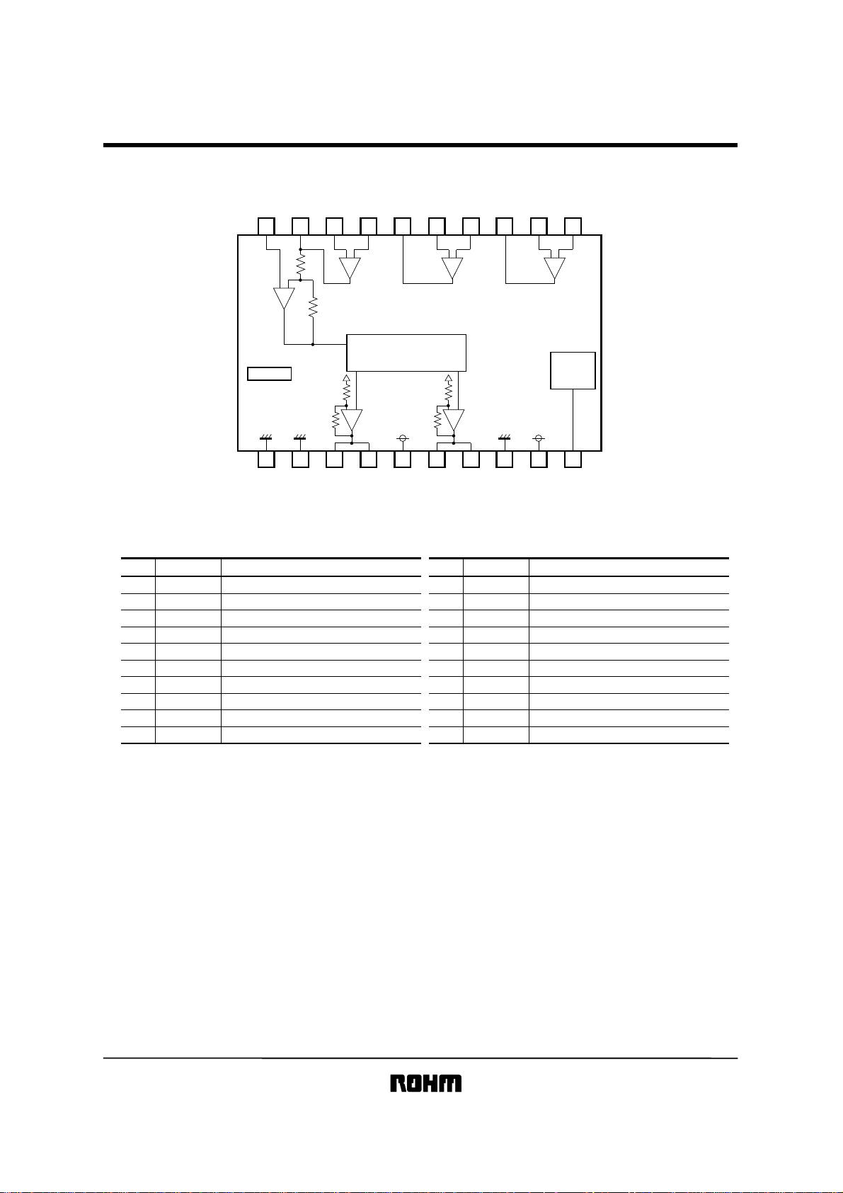
Block diagram
BA5961FV
11
12
13
14
15
16
17
18
19
20
−
+
TSD
Pre
Pow
GND
GND 1
2
1
!!!!Pin descriptions
Pin No. Pin name Functions
10
1
2
3
4
5
6
7
8
9
PreGND
PowGND1
OUT+
OUT+
PowV
OUT−
OUT−
PowGND2
PreV
STBY
Pre ground
Power ground (For positive output)
Driver positive output
Driver positive output
Powerblock power supply
CC
Driver negative output
Driver negative output
Power ground (For negative output)
Pre block power supply
CC
Stand-by control input
Pre
V
CC
9
−
+
STAND-BY
10
−
+
IN
LEVEL SHIFT
+
−
+
Pow
V
CC
5
4
3
−
+
−
−
+
Pow
GND 2
8
7
6
TSD : Thermal shut down
Pin No. Pin name Functions
11
12
13
14
15
16
17
18
19
20
OP3+
OP3−
OP3OUT
OP2+
OP2−
OP2OUT
OP1+
OP1−
IN
BIAS
OP-AMP3 positive input
OP-AMP3 negative input
OP-AMP3 output
OP-AMP2 positive input
OP-AMP2 negative input
OP-AMP2 output
OP-AMP1 positive input
OP-AMP1 negative input
OP-AMP1 output and driver input
Bias input
2/7
Optical disc ICs
!!!!
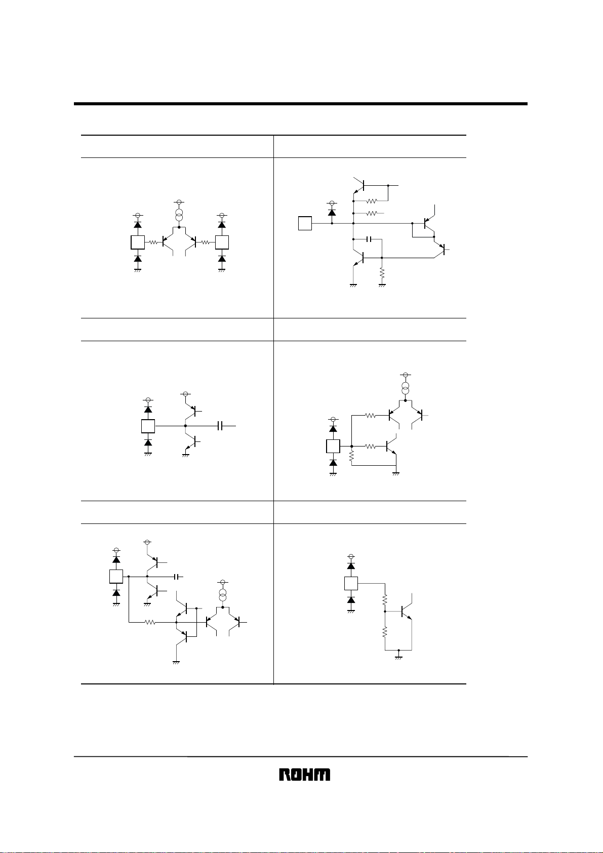
Input output circuits
BA5961FV
positive input
11, 14, 17pin
Pre V
13, 16pin
OP-AMP input
CC
OP-AMP output
Pre V
CC
Pre V
Pre V
Driver output
CC
Pre V
CC
1k1k
negative input
12, 15, 18pin
positive
output
3, 4pin
negative
output
6, 7pin
Pow V
CC
10k
10k
10k
BIAS input
Pre V
CC
CC
Pre V
20pin
24.3k
CC
50k
100k
Pre-OP-AMP output and driver input Stand-by control input
Pre V
19pin
24.3k
CC
Pre V
CC
Pre V
CC
10pin
Pre V
CC
100k
100k
3/7

BA5961FV
Optical disc ICs
!!!!Electrical characteristics (unless otherwise noted, Ta=25°C, PreVCC=PowVCC=5V, VBIAS=1.65V, RL=8Ω)
Parameter
Quiescent current without signal
<Driver block>
Output offset voltage
Maximum output voltage amplitude
Maximum output voltage amplitude (
Separated voltage supply
Closed circuit gain
Srand-by ON voltage
Srand-by OFF voltage
<Operational amplifier>
Offset voltage
Input bias current
Common mode input range
High level output voltage
Low level output voltage
Output drive current(Sink)
Output drive current(Sorce)
Slew rate
This product in not designed for protection against radioactive rays.
Symbol Min. Typ. Max. Unit Conditions
mA
14.0
−60
3.0
3.5
16.0
2.0
−6
0.1
4.1
0.5
0.5
10.0
−
V
mV
60
−
−
3.6
−
4.2
20.0
18.0
0.5
−
−
−
−
6
0
300
30
−
3.8
−
−
4.8
0.9
0.2
−
−
−
−
−
−
1
−
IN
=
BIAS=
V
V
PreV
CC
=12V, PowVCC=5V
dB
IN
=1.35V, 1.95V
V
V
V
mV
nA
V
V
V
IN
=
GND, Invert amp.
V
VIN=V
CC
, Invert amp.
mA
mA
V / µs
100kHz square wave, 2Vpk-pk
1.65V
Q
I
V
OOF
V
OM
)
V
OMS
G
VC
V
STON
V
STOFF
V
OFOP
I
BOP
V
ICM
V
OH
V
OL
I
SI
I
SO
SROP
Measuring
circuit
Fig.1
Fig.1
Fig.1
Fig.1
Fig.1
Fig.1
Fig.1
Fig.1
Fig.1
Fig.1
Fig.1
Fig.1
Fig.1
Fig.1
Fig.1
4/7

Optical disc ICs
!!!!Measuring circuit
VBIAS
OPOUT
BA5961FV
OPIN−
OPIN+
OPOUT
OPIN−
OPOUT
OPIN−
OPIN+
OPIN+
V
1.65V
14151617181920
111213
BA5961FV
7654321 1098
0.1µ
A
1M
10k
IQ
VST
CC
=5V
V
OPOUT
V
VOOP
V
ISO
ISI
3
OPRL
1
2
RL
8
V
VO
OPIN+
OPB
3
1M
VIOF
V
1
2
OPBIAS
OPIN
OPIN−
1
10k
2
0.1µ0.1µ
VBOP
NF
3
1
2
Fig.1
VIN
5/7

Optical disc ICs
1. Switch table
(1) Driver (VBIAS=OPBIAS=1.65V, OPIN→2, NF→2, OPRL→1)
BA5961FV
Symbol
IQ
Voof
VOM
GVC
VSTON
VSTOFF
Switch
RL VIN
OFF
ON
ON
ON
ON
ON
−
1.65V
∗
1
±0.3V
5V
5V
Input
VST
2.0V
2.0V
∗
1
2.0V
2.0V
0.5V
2.0V
VIN=0V and 5V
VIN=1.35V and 1.95V
(2) OP-AMP (VST=2.0V, VBIAS=1.65V, RL→OFF)
Symbol
VOFOP
IBOP
VOHOP
VOLOP
ISI
ISO
SROP
!!!!
Application example
OPB NF
Switch
OPRL OPIN OPBIASVIN
1
1
1
1
3
1
1
2
1
1
2
1
1
1
3
1
1
2
2
1
1
Input
1
−
1.65V
1
−
1.65V
2
0V
2.5V
5V
2
1
1
1
2.5V
−
1.65V
−
1.65V
−
±1V
Measuring point
IQ
VO
VO
VO
VO
VO
VBIAS=2.5V
VBIAS=2.5V
ISI=0.5mA
ISO=0.5mA
100kHz square wave, 2Vp-p input
Measuring point
VIOF
VBOP / 1MΩ
VOOP
VOOP
VIOF
VIOF
VOOP
10k
10k
SIGNAL BIAS
BA5961FV
0.1µ
M
LOAD
Fig.2
SERVO PRE AMP
14151617181920
7654321 1098
STAND-BY
CC
V
111213
0.1µ
6/7

BA5961FV
Optical disc ICs
!!!!Operation notes
1. A thermal-shutdown circuit (over-temperature protection circuit) is built in to prevent the IC from thermal breakdown.
Use the IC under the thermal loss allowed to the package. In case the IC is left running over the allowable loss, the
junction temperature rises, and the thermal-shutdown circuit works at the junction temperature of 175°C (typ.)
(the outputs of the driver is turned off). When the junction temperature drops to 150°C (typ.), the IC start operating
again.
2. When stand-by control terminal (Pin 10) drops below 0.5V, stand-by mode is established. Make sure that under normal
operating conditions, this pin at 2.0V or above.
3. If PreV
returns to its previous state.
4. If the bias pin (Pin 20) drops below 0.7V, the output is muted. Make sure that under normal operating conditions, this
pin is at 1.0V or above.
5. The output is muted in the event of a thermal shut down, mute-on, or a bias and Pre-V
is muted. When muted, the internal bias voltage of the output pin becomes roughly (Pow V
6. Please connect a bypass capacitor (0.1µF) across the supply voltage lines close to the IC pins.
7. When a capacitance load is connected to the OP amplifier output, the amplifier phase margin decreases, which causes
the peak or oscillation. When connecting such load, insert a resistance in series between the output and the
capacitance load and take a full consideration for frequency characteristics to prevent problem during practical use.
8. Do not short-circuit between any output pin and supply pin (supply fault) or ground (ground fault), or between any
output pins (load short-circuit). When mounting the IC on the circuit board, be extremely cautions about the orientation
of the IC. If the orientation is mistaken, the IC may break down, and produce smoke in some cases.
(Pin 9) drops below 3.4V (typ.), the driver is turned off. When the voltage exceeds 3.6V (typ.) the driver
CC
voltage drop. Only the driver
CC
-Vf) / 2).
CC
!!!!Electrical characteristics curve
1.5
1.0
0.5
POWER DISSIPATION : Pd (W)
0
0 25 50 75 100
AMBIENT TEMPERATURE : Ta (°C)
On less than 3%
(percentage occupied by copper foil),
70mm×70mm, t=1.6mm
glass epoxy mounting.
125 150 175
Fig.3 Power dissipation
!!!!External dimensions (Units : mm)
6.5±0.2
20 11
6.1±0.2
8.1±0.3
1
1.7±0.2
0.65
0.11
0.22±0.1
0.3Min.
10
0.15±0.1
0.1
SSOP-B20W
7/7
 Loading...