ROHM BA5417 Datasheet

BA5417
Audio ICs
High-output dual power amplifier
BA5417
The BA5417 is a 6 to 15V-compatible dual power amplifier developed for use radio cassette players. It is equipped with
standby switching functions for excellent total harmonic distortion and other basic characteristics.
Applications
!
Radio cassette / Mini compo players
Features
!
1) High output.
OUT
P
= 2.8W (VCC = 9V, RL 3Ω, THD = 10%)
OUT
P
= 5.0W (VCC = 12V, RL 3Ω, THD = 10%)
2) Excellent audio quality
THD = 0.1% (f = 1kHz, P
NO
V
= 0.3mVrms (Rg = 10kΩ)
RR = 55dB (f
RR
= 100Hz)
O
= 0.5W)
3) Wide supply voltage operating range
CC
(V
= 6.0V to 15.0V).
4) Switching noise (“pop” noise) generated when the
power is switched on and off is small.
5) Ripple mixing when motor starts has been prevented.
6) Built-in thermal shutdown circuit.
7) Built-in standby switch. Output is not influenced by
the standby pin voltage.
8) Soft clipping.
Absolute maximum ratings
!!!!
Parameter Symbol Limits Unit
Power supply voltage V
Power dissipation Pd
Operating temperature Topr −20 ~ +75 °C
Storage temperature Tstg −55 ~ +150 °C
1 Must be within standby values.
∗
2 Ta=75
°C(
∗
Recommended operating conditions
!!!!
when using infinite heatsink)
Parameter Symbol Limits Unit
(Ta = 25°C)
CC
CC
V
(Ta = 25°C)
6.0 ~ 15.0
20
15
1
∗
2
∗
V
W
VPower supply voltage

Audio ICs
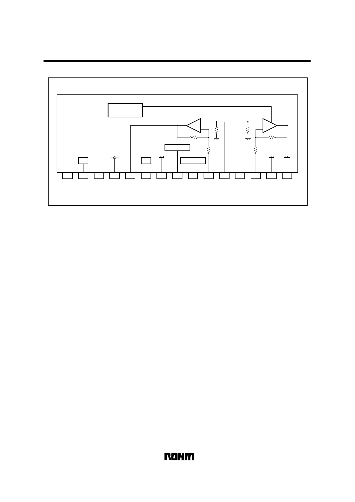
Block diagram
!!!!
T . S . D
BA5417
+
30k
−
30k
+
−
CC
V
B S B S F I L T E R
GND
1 2
(N.C.)
3 4 5 6 7 8 9 10 11 12 13 14 15
CC
OUT2
V
OUT1
BS2
POWER
BS1
POWER-GND
S T . B Y
STBY
30k
FILTER
NF1
30k
45
IN1
IN2
45
GND1
PRE
NF2
PRE-GND1
GND2
PRE
PRE-GND2

Audio ICs
Electrical characteristics
!!!!
_ (unless otherwise noted, Ta=25°C, Vcc=9.0V, R
Parameter Symbol Min. Typ. Max. Unit Coniditions
Quiescent current
Rated output voltage 1
Rated output voltage 2
Closed-loop voltage gain
Output noise voltage
Total harmonic distortion THD − 0.1 1.0 %
Ripple rejection RR 42 55 − dB
Crosstalk CT 48 65 −
Circuit current
(with standby switch off)
Standby pin current when on
Standby pin
control voltage
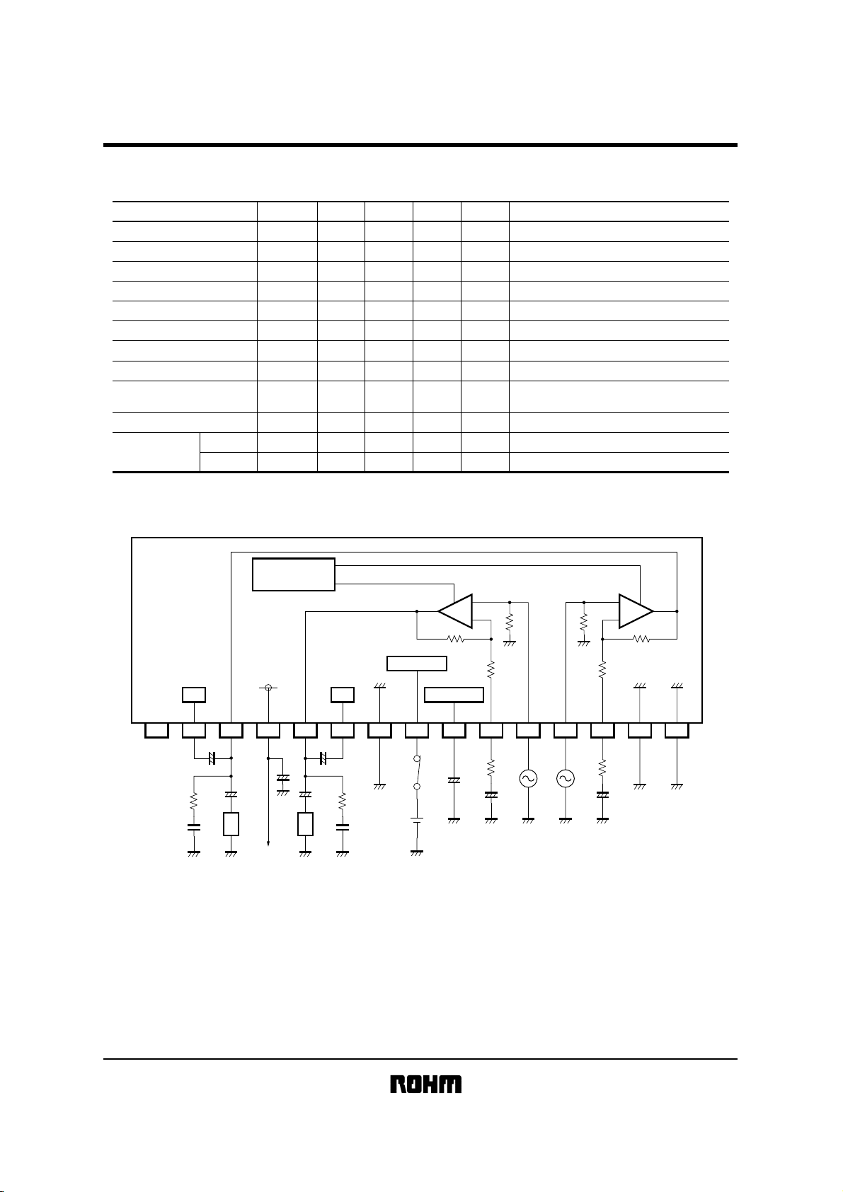
Measurement circuit
!!!!
Activated
Not activated
O
I
P
OUT
1
P
OUT
2
VC
G
NO
V
I
OFF
I
SIN
V
STH
V
STL
L
=3Ω, RF=120Ω, Rg=600Ω, f=1kHZ, OTL mode)
−
22 45 mA
2.2 2.8 − W
4.0 5.0 − W
43
−
45 47 dB
0.3 1.0 mVrms
− 020µA
− 0.15 0.4 mA
3.5
−
−−−1.2 V −
dB
V
IN
=
0Vrms
V
TDH=10%
TDH=10%, V
=
10kΩ, DIN AUDIO
Rg
OUT
=
0.5W
P
f
RR
=
100Hz, V
O
=
0dBm
V
STBY
=
V
CC
V
CC
=
RR
=
BA5417
12V
−
−10dBm
−
−
T . S . D
CC
V
B S B S F I L T E R
R
2.2
C
7
0.15µ
POWER
2
1 2
(N.C.)
R
2.2
0.15µ
3 4 5 6 7 8 9 10 11 12 13 14 15
C
C
2
+
100µ
+
1
C
1
C
3
1000µ
R L
1000µ
+
1000µ
6
+
C
100µ
4
C
5
+
R L
GND
∗
S T . B Y
1
Fig.1
+
30k
−
30k
45
F1
+
R
C
8
120
+
C
9
47µ
47µ 47µ
+
30k
−
30k
45
GND1
PRE
R
F2
120
+
C
10
1 V
STBY
∗
GND2
PRE
=3.5V ~ V
CC
 Loading...