ROHM BA51W12SAT Datasheet

BA51W12SAT
Regulator ICs
Dual output voltage regulator with power
saving
BA51W12SAT
The BA51W12SAT is a general-purpose, low saturation power supply with two outputs : 9V, 1A and 5V, 500mA. The IC is
available in a compact TO220FP-5 package. The outputs can be turned off during the power saving state with the built-in
switch. Also built in the IC is an overcurrent protection circuit, an overvoltage protection circuit, and a thermal shutdown
circuit.
!!!!Applications
Car audio systems, VCRs, facsimiles, air conditioners, and other household and industrial equipment
!!!!Features
1) Minimum I / O voltage differential is 0.5V or less.
2) Built-in protection circuits against overcurrent, over voltage, and overheat.
3) Available in a compact TO220FP-5 package (pins are bendable).
4) Zero power saving current. (Typ.)
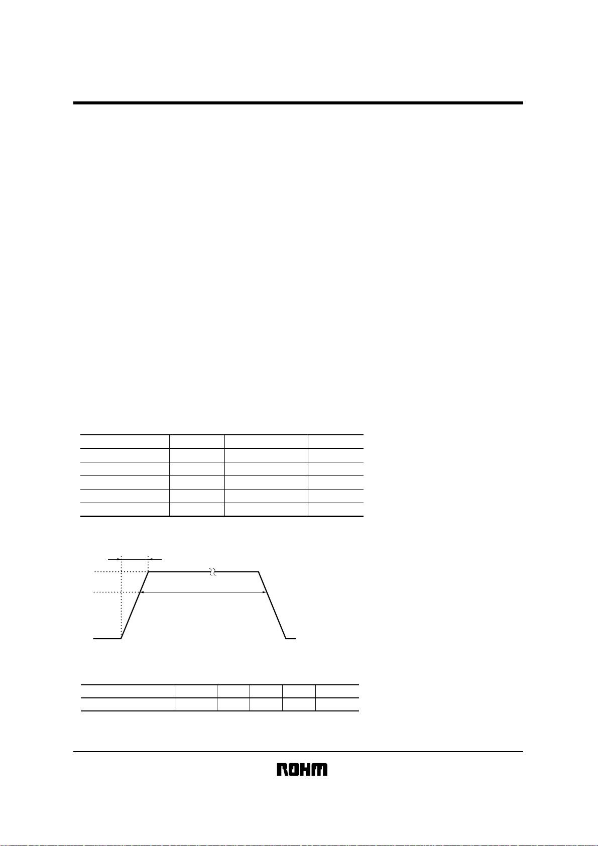
!!!!Absolute maximum ratings (Ta=25°C)
Parameter Symbol Limits Unit
Power supply voltage
Power dissipation
Operating temperature
Storage temperature
Peak applied voltage
∗1
Reduced by 16mW for each increase in Ta of 1°C over 25°C.
∗
2 Applied time is less than 200 ms (tr≥1ms).
tr≥1ms
50V
35V
0V
VCC 35 V
1
∗
Pd
Topr −40~+85 °C
Tstg −55~+150 °C
VCCPeak 50
Max.200ms
2000
2
∗
!!!!Recommended operating conditions (Ta=25°C)
Parameter
Power supply voltage V
Symbol Min. Typ. Max. Unit
CC
10 25 V14
mW
V

Regulator ICs
!!!!
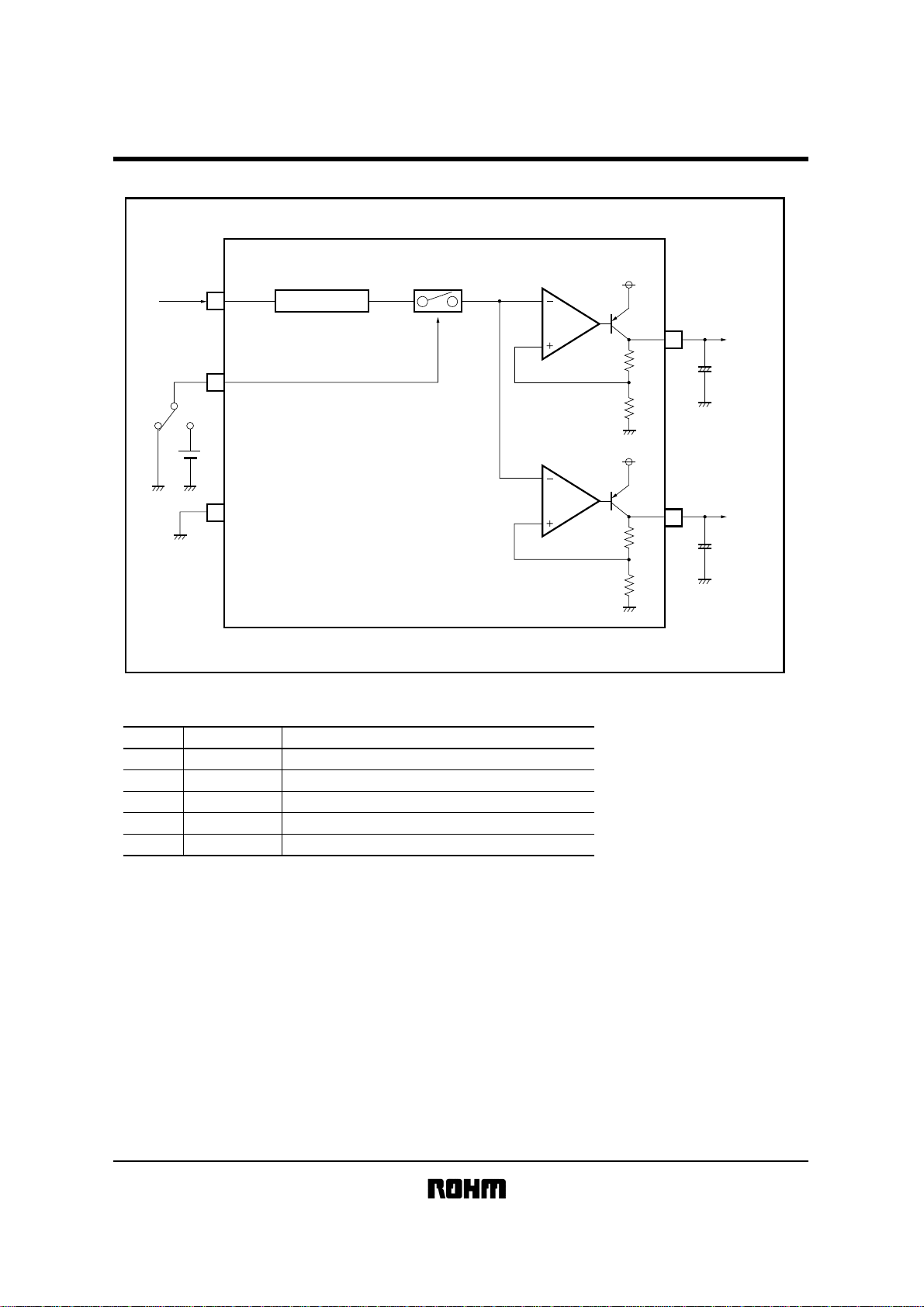
Block diagram
V
CC
2
CTL
5
REFERENCE VOLTAGE
BA51W12SAT
9V
1
OUT1
+
GND
3
!!!!Pin descriptions
Pin No.
1
2
3
4
5
Pin name
OUT1
GND
OUT2
V
CC
CTL
Output1 (9V, 1A)
Power supply
Ground
Output2 (5V, 500mA)
ON / OFF switch
Function
5V
4
OUT2
+

Regulator ICs
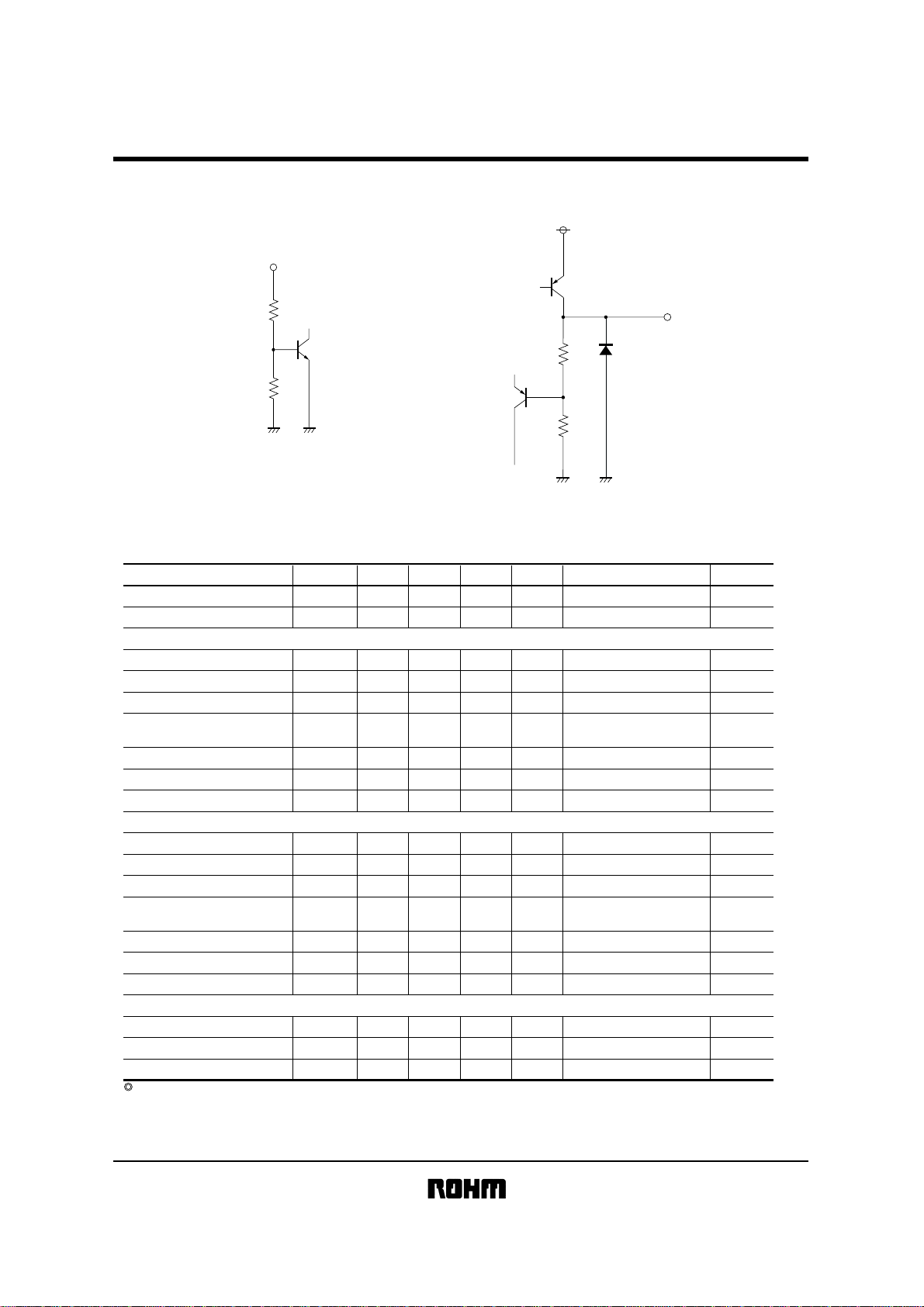
!!!!Input / output circuits
CTL (5pin)
OUT1, 2
CC (2pin)
V
BA51W12SAT
25k
25k
GND (3pin)
12.4k (1pin)
6k (4pin)
2k
GND (3pin)
1, 4pin
!!!!Electrical characteristics (unless otherwise noted, Ta=25°C, VCC=14.0V)
Conditions Test circuit
OFF mode
ON mode
I
O1
=500mA
I
O1
=500mA VCC=8.55V
O1
=500mA, f=120Hz
I
IN
=1V
rms
e
VCC=10→25V, IO=500mA
I
O
=5mA→1A
CC
=25V
V
O2
=350mA
I
I
O2
=350mA VCC=4.75V
O2
=350mA, f=120Hz
I
IN
=1V
rms
e
VCC=6→25V, IO=350mA
I
O
=5mA→500mA
V
CC
=25V
Output ACTIVE mode
Output OFF mode
th
=5V
V
Fig.4
Fig.4
Fig.1
Fig.3
Fig.1
Fig.2
Fig.1
Fig.1
Fig.5
Fig.1
Fig.3
Fig.1
Fig.2
Fig.1
Fig.1
Fig.5
Fig.6
Fig.6
Fig.7
0
Max. Unit
10 µA
5.0 mA
Parameter
Power save supply current
Bias current
Symbol
I
ST
I
b
Min.
-
-
Typ.
3.0
<9V output section> (Output 1)
Output voltage 1
Minimum I / O voltage differential 1
Output current capacity 1
Ripple rejection ratio 1
Input stabillty 1
Load regulation 1
Output short-circuit current 1
V
O1
∆V
O1
I
O1
R.R1
Reg.I1
Reg.L1
I
OS1
8.55
-
1.0
-
-
-
-
9.0
0.3
55
50
100
150
-
9.45 V
0.5 V
-A
-dB
100 mV
150 mV
-mA
<5V output section> (Output 2)
Output voltage 2
Minimum I / O voltage differential
2
Output current capacity 2
Ripple rejection ratio 2
Input stabillty 2
Load regulation 2
Output short-circuit current 2
V
O2
∆V
O2
I
O2
R.R2
Reg.I2
Reg.L2
I
OS2
4.75
-
500
-
-
-
-
5.0
0.3
60
50
50
100
-
5.25 V
0.5 V
-mA
-dB
100 mV
100 mV
-mA
<Switch section>
ON mode voltage
OFF mode voltage
Input high level current
Not designed for radiation resistance.
Note) All the characteristic values are measured with a 0.33µF-capacitor connected the input pin and 22µF-capacitor connected to the output pin.
Measurements are made by using a plus (tw≤10ms, duty cycle≤5%) in all cases but noise voltage and the ripple rejection ratio.
V
th
V
th
I
IN
2.0
1
2
-
-
-
-
150
-V
0.8 V
- µA
 Loading...