

Regulator ICs
Power supply for CD radio cassette
players
BA3924
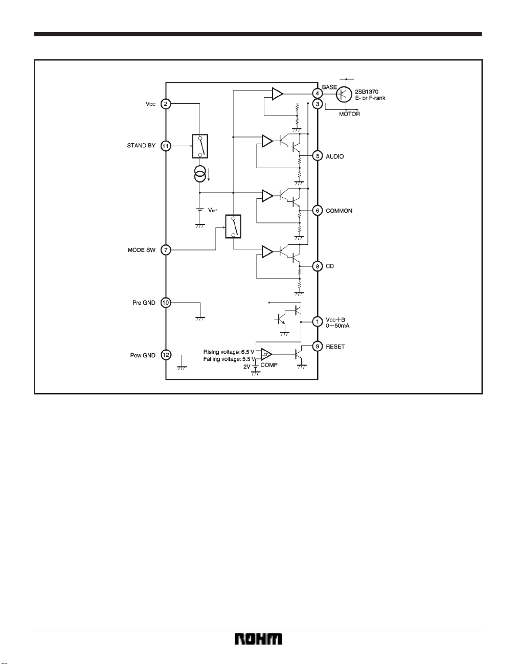
The BA3924 is a system reference power supply for use in CD radio cassette players. Outputs dedicated to a microprocessor (5.0V), CD player (7.5V), audio system (7.5V), and motor drive (9V) are built in. Also built in is a V
that allows turning ON and OFF the supply voltage by HIGH and LOW levels of the standby pin.
Applications
CD radio cassette players
Features
1) With outputs dedicated to a microcontroller, CD player, audio system, and motor drive, the IC is best
suited for CD radio cassette players.
2) Zero standby current (typ.).
3) Output current limit circuit protects the IC against
short-circuiting damage.
4) Compact 12-pin package allows large power dissipation.
5) Thermal shutdown circuit protects the IC against
thermal damage.
6) V
CCB output allows turning ON and OFF the power
supply voltage by HIGH and LOW levels of the standby pin.
CCB output
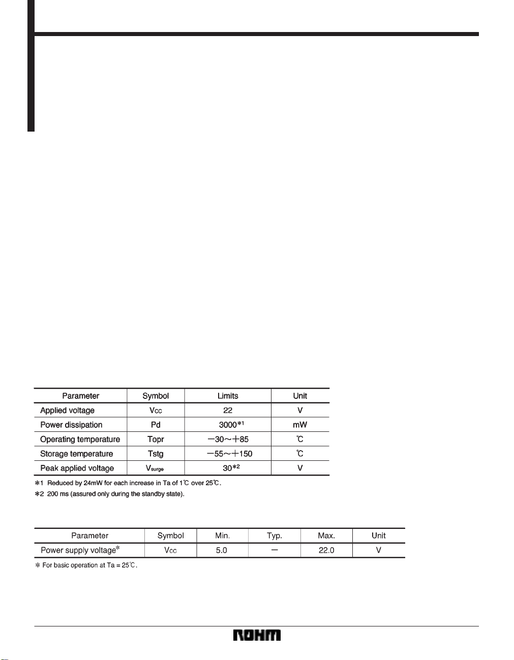
Absolute maximum ratings (Ta = 25C)
Recommended operating conditions (Ta = 25C)
141
Regulator ICs BA3924
Block diagram
142
Regulator ICs BA3924
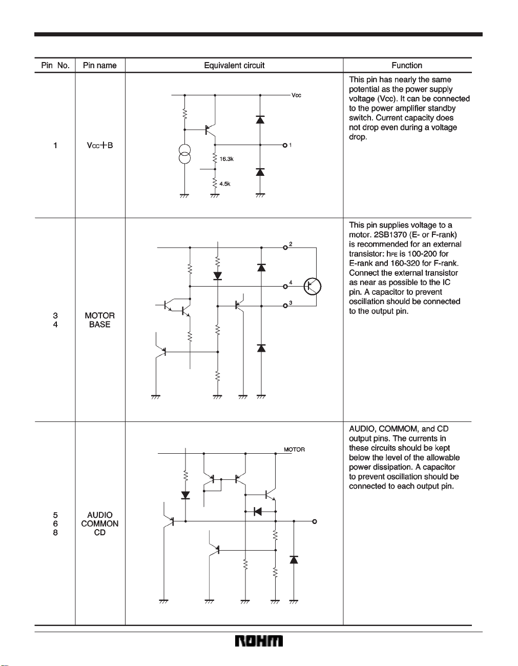
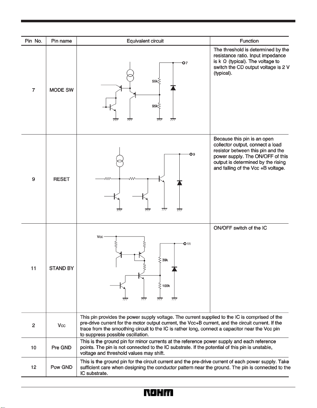
Pin descriptions
143
Regulator ICs BA3924
144

Regulator ICs BA3924
Electrical characteristics (unless otherwise noted, Ta = 25C, VCC = 12V)
145

Regulator ICs BA3924
146

Regulator ICs BA3924
Measurement circuits
147

Regulator ICs BA3924
Circuit operation
148

Regulator ICs BA3924
Application example
149

Regulator ICs BA3924
FOperation notes
(1) Operating power supply voltage
When operating within the proper ranges of power supply
voltage and ambient temperature, most circuit functions
are guaranteed. Although the rated values of electrical
characteristics cannot be absolutely guaranteed, characteristic values do not change drastically within the
proper ranges.
When the supply voltage becomes less than the sum of
the minimum I / O voltage differential and each output
voltage, the reference power supply will not function any
more. However, there will be no sudden drop in voltage
or output current.
(2) Power dissipation (Pd)
Refer to the power dissipation characteristics (Fig. 7) and
the rough estimation of IC power dissipation given on a
separate page. Make sure to consider the power dissipation of the external PNP transistors, through which power
is supplied to the AUCIO, CD, and COMMON circuits.
Leave a sufficient margin in your application.
S Power dissipation
Except under transitional conditions, the power dissipation of this IC is 3W per unit at 25_C. Use the following
equations and Fig. 1 to roughly calculate the allowable
power dissipation and decide if a heat sink is needed or
what kind of a heat sink is needed.
(Basic equation)
Pd = P * P
O
where
P = power supplied from the power supply
O = power supplied to the load from the IC
P
(Rough estimation)
S Power consumed by the AUDIO output
P1 = (VOMO * VO1) IO1
S Power consumed by the CD output
2 = (VOMO * VO2) IO2
P
S Power consumed by the COMMON output
3 = (VOMO * VO3) IO3
P
S Power consumed by the VCC+B output
4 = (VCC * VO4) IO4
P
S Power consumed by the circuit current
5 = VCC IQ
P
S Power consumed by the MOTOR output
where
P
6 = (VCC * VF) IBMO
Pd = P1 ) P2 ) P3 ) P4 ) P5 ) P6
VCC is the maximum constant supply voltage
OMO is the minimum MOTOR output voltage
V
O1 is the minimum AUDIO output voltage
V
O2 is the minimum CD output voltage
V
O3 is the minimum COMMON output voltage
V
O4 is the minimum VCC)B output voltage
V
V
CC * VF = (minimum constant supply voltage)
* 0.7V
Q is the maximum circuit current
I
O1 is the maximum AUDIO constant output
I
current
O2 is the maximum CD constant output current
I
I
O3 is the maximum COMMON constant
output current
O4 is the maximum VCC)B constant
I
output current
O5 is the maximum constant base drive current
I
150

Regulator ICs BA3924
(3) Preventing oscillation at each output
T o stop output oscillation, make sure to connect a capacitor between GND and each of the MOTOR (pin 3), AUDIO (pin 5), COMMON (pin 6), and CD (pin 8) output
pins. Use capacitors whose valve are not below the values denoted in the application circuit (Fig. 4) and not susceptible to temperature.
(4) Ground pins
Pre GND (pin 10) and Pow GND (pin 12) are the ground
pins of the IC. Pin 10 is the reference ground pin for power supplies, including the built-in reference power supply,
and the comparators. Voltage and threshold values may
shift if the potential of pin 10 is unstable. Take sufficient
care when designing the conductor pattern near this pin.
The source current from this pin is in the level of a few milliamperes. Pin 12, which is connected to the ground
traces other than those connected to pin 10, is connected
with the IC substrate and the back metal.
(5) External PNP transistors
ROHM’s 2SB1370 (E- or F-rank) is recommended. This
is a TO-220FP type transistor.
(6) Overvoltage protection circuit
Although the absolute maximum voltage is 22V, a peak
voltage of 30V for 200ms is assured only during the
standby state (pin 1 1 is LOW). The overvoltage circuit is
activated when the V
circuit is activated, a standby circuit current (IST) of a few
milliamperes flows in the IC.
The overvoltage protection circuit is also activated if a
voltage exceeding the absolute maximum rating is applied while the ST ANDBY pin is HIGH. As a result all the
output voltage is turned off.
CC voltage exceeds 23V. When the
(7) Overcurrent protection circuit
If the output current of any of the MOTOR (pin 3), AUDIO
(pin 5), COMMON (pin 6), and CD (pin 8) exceeds the
current capacity, the built-in current limit circuit limits the
current to a set level. If the potential of each pin is about
the same as that of Pow GND (pin 12), the output current
is reduced to the level of the ground short-circuit current
given in the “Electrical Characteristics.”
(8) Thermal protection
The circuit current, the limit current of each power supply
output, and the ground short-circuit current decrease
gradually with increasing temperature. For further
protection, the thermal shutdown circuit turns off all outputs when the IC is overheated, and brings back to normal operation when the temperature is decreased to a
certain level.
151

Regulator ICs BA3924
Electrical characteristic curve
External dimensions (Units: mm)
152
 Loading...