BA3880AS / BA3880AFS
Audio ICs
High-definition sound processor
BA3880AS / BA3880AFS
The BA3880AS and BA3880AFS are sound processor ICs that perform phase and harmonic compensation on audio
signals to accurately reproduce the "rise" section of audio signals that determines the characteristics of the sound, and
thus reproduce the original recording as naturally as possible.
Applications
!!!!
Component stereo systems, radio cassette players, car stereo systems, televisions, VCRs, and active speakers.
Features
!!!!
1) Correct distortion in the rising section of audio signals that results from miss-matched speakers and amplifiers, and
reproduces the original sound faithfully.
2) To allow application with all types of speakers and sources, the clarity can be adjusted using DC control.
3) DC control provided for selection of either processor mode or bypass mode.
4) Bass boost fixed internally to 4dB.
Block diagram
!!!!
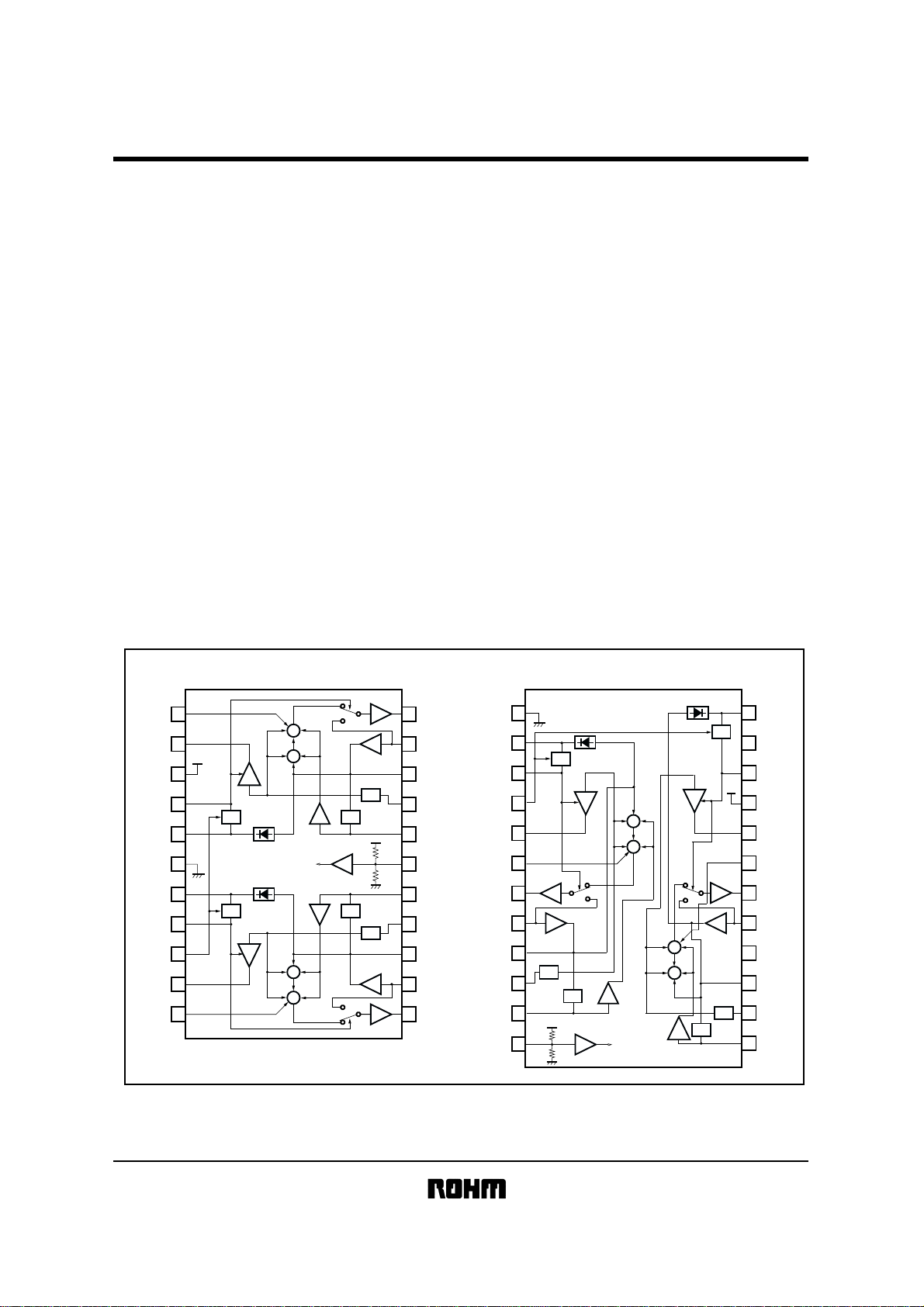
BA3880AS
1
MIXL
2
VCAL
3
CC
V
4
DEFL
5
DETL
6
GND
7
DETR
8
DEFR
CTL
9
10
VCAR
11
MIXR
CTL
CTL
VCA
VCA
+
+
+
+
+
HI MID LO
+
+
+
−
−
+
+
+
HI
+
MID
+
+
+
+
BA3880AFS
CTL
HPF
24
DETL
23
22
DEFR
21
CC
V
20
VCAL
19
MIXL
18
OUTL
17
INL
16
15
APFL
14
HPFL
13
LPFL
1
22
OUTL
21
INL
20
APFL
HPF
19
LPF
LPF
HPF
LO
HPFL
18
LPFL
17
BIASC
16
LPFR
15
HPFR
APFR
14
13
INR
OUTR
12
GND
DETR
DEFR
CTL
VCAR
MIXR
OUTR
INR
APFR
HPFR
LPFR
BIASC
2
CTL
3
VCA
LO
−
+
+
+
+
+
+
+
+
HI
MID
LO
+
+
+
−
LPF
HPF
LPF
VCA
+
+
HI
MID
+
+
+
4
5
6
7
8
9
10
11
12

Audio ICs
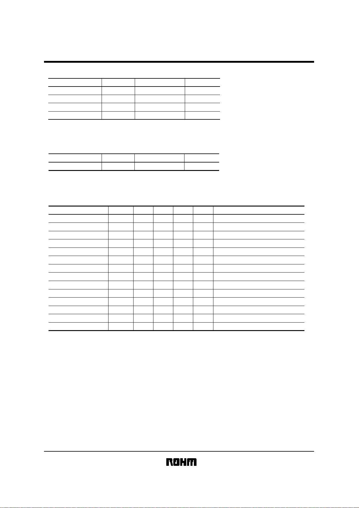
Absolute maximum ratings
!!!!
Parameter
Power supply voltage
Power dissipation
Operating temperature
Storage temperature
Reduced by 10mW for each increase in Ta of 1°C over 25°C.
∗
Recommended operating conditions
!!!!
(Ta = 25°C)
Symbol Limits Unit
CC
V
Pd
Topr
Tstg
11
∗
1000
−40~+85
−55~+125
BA3880AS / BA3880AFS
V
mW
°C
°C
Parameter
Power supply voltage V
Electrical characteristics
!!!!
(unless otherwise noted, Ta = 25°C, V
Parameter
Circuit current
Voltage gain 1
Voltage gain 2
Voltage gain 3
Voltage gain 4
Voltage gain 5
Channel balance
Maximum output voltage
Output noise voltage 1
Output noise voltage 2
Total harmonic distortion 1
Total harmonic distortion 2
Channel separation
Ripple rejection ratio
∗Note : When VCTL = 9V, the IC is in bypass mode (through operations).
When V
CTL = 4.5V, the IC is in processor mode (enhance operations) with minimum definition level.
CTL = 0V, the IC is in processor mode (enhance operations) with maximum definition level.
When V
Symbol Limits Unit
CC
Symbol
I
CC
G
V1
G
V2
G
V3
G
V4
G
V5
5.4~10.8 V
CC
= 9V, fIN = 1kHz, VIN = 200mVrms, Rg = 600Ω, RL = 100k Ω and V
Min.
3.9
Typ.
5.9
−2.0
−2.5
−1.0
9.0
−0.5
1.0
11.0
−
4.0
CB −2.0 0 2.0 dB
V
V
NO1
V
NO2
THD
THD
OM
2.0 2.3 − Vrms THD
− 210µVrms
− 16 70 µVrms
1
− 0.005 0.05 % 400Hz~30kHz BPF,
2
− 0.04 0.4 % 400Hz~30kHz BPF
CS −−67 −60 dB
RR 60 68 − dB
Max. Unit Conditions
11.8
0
2.0
1.5
4.0
13.0
−
mA
dB
dB
dB
dB
dB
IN
=
0Vrms
V
V
CTL
= 9V
fIN = 10kHz
IN
= 10kHz, V
f
IN
= 50Hz
f
fIN = 10kHz, V
=
1%
Rg = 0Ω, DIN AUDIO, V
Rg = 0Ω, DIN AUDIO
VIN = 1Vrms
Rg = 0Ω, fR = 100Hz, VR = 100mVrms
CTL
CTL
= 0V
= 0V
CTL
= 4.5V)
CTL
= 9V
V
CTL
=
9V

Audio ICs
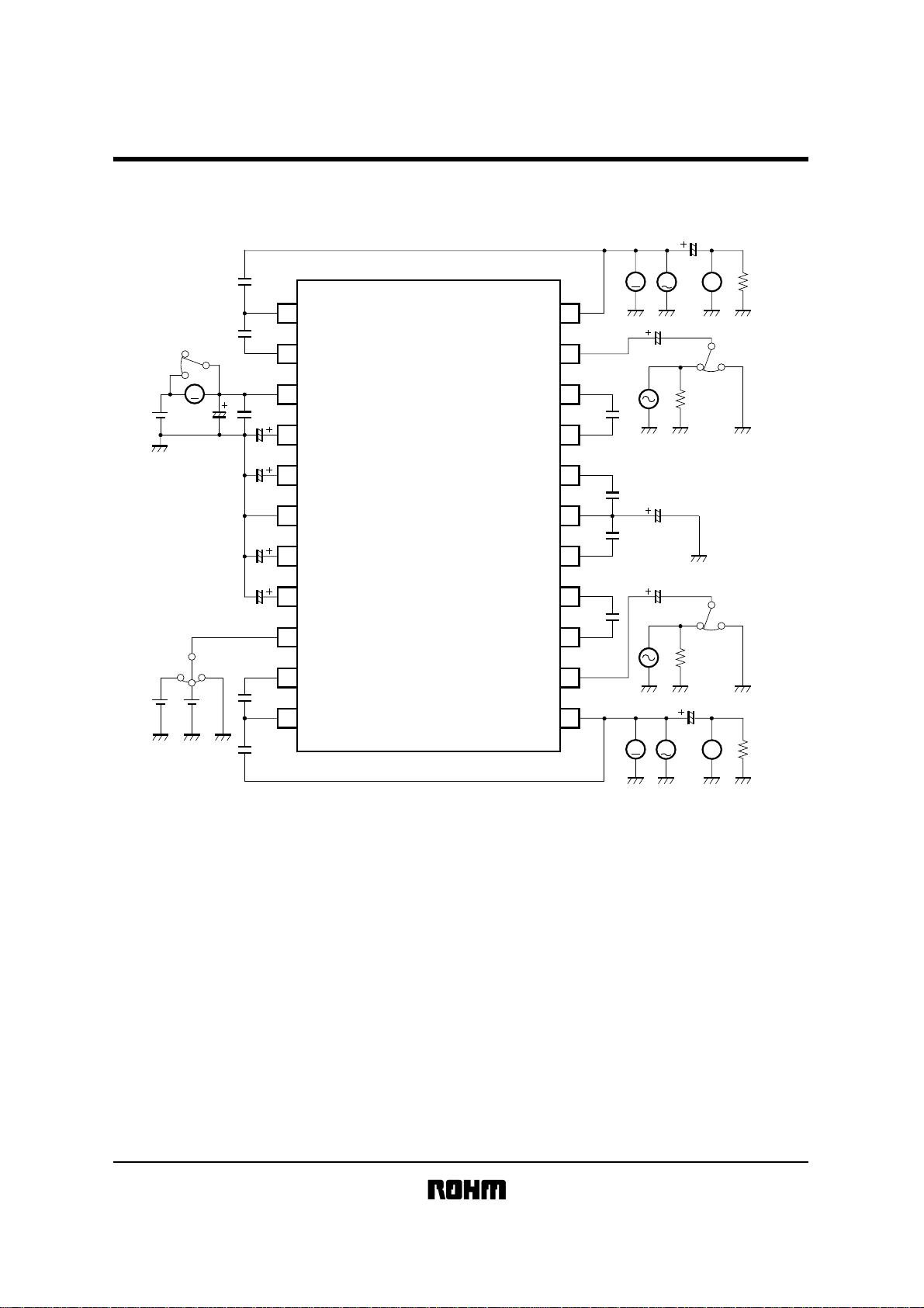
Measurement circuit
!!!!
BA3880AS
470p
6800p
BA3880AS / BA3880AFS
1 22
MIXL
2 21
VCAL
OUTL
INL
4.7µ
V
V
4.7µ
THD
100k
A
9V
9V 4.5V
47µ
3 20
CC
V
0.1µ
4 19
1µ
4.7µ
4.7µ
1µ
470p
6800p
DEFL
DETL
5 18
GND
6 17
7 16
DETR
8 15
DEFR
9 14
CTL
10 13
VCAR
11 12
MIXR
BA3880AS
Fig.1
APFL
HPFL
LPFL
BIASC
LPFR
HPFR
APFR
INR
OUTR
0.01µ
0.068µ
0.068µ
0.01µ
600
47µ
4.7µ
600
4.7µ
V
V
(Units) R : Ω
THD
C : F
100k
 Loading...