

ROHM BA3836 Datasheet
1
Multimedia ICs
Vocal fader IC
BA3836
Realizes karaoke functionality by enabling you to erase only the vocals from commercially available music software.
•
Applications
Mini-components, radio cassette players, car stereos,
karaoke sets
•
Features
1) Vocal fader functions (erase vocals from commer-
cially available music software) all on one chip.
2) Has internal secondary active LPF to enable a high-
degree of vocal cancellation (synchronous rejection
ratio) while retaining the same feeling.
3) Three control pins for switching between 4 modes:
through, vocal fader, sound multiplexing, and mute.
4) Key controller input and internal switches.
5) Internal microphone amplifier.
6) Low noise and low distortion.
7) Few external components.
•
Absolute maximum ratings (Ta = 25°C)
Parameter Symbol Limits Unit
Power supply voltage
Power dissipation
Operating temperature
Storage temperature
V
CC Max.
Pd
Topr
Tstg
18
1000
∗
1
– 40 ~ + 85
– 55 ~ + 125
V
mW
°C
°C
∗
1 Reduced by 10mW for each increase in Ta of 1°C over 25°C when mounted.
•
Recommended operating conditions (Ta = 25°C)
Parameter Symbol UnitMax.Typ.Min.
Power supply voltage
V
CC 5.4 10—V
2
Multimedia ICs BA3836
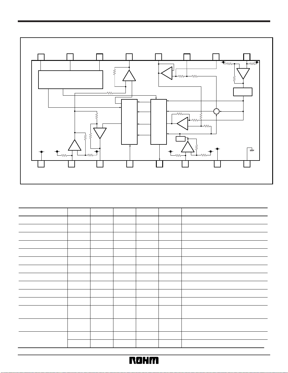
•
Electrical characteristics (unless otherwise noted, Ta = 25°C, VCC = 10V, fIN = 1kHz, VIN = 150mV, RL = 100kΩ)
Parameter Symbol Min. Typ. Max. Unit
I
Q 1.6 2.6 3.3 mA
V
om 2.3 2.8 — Vrms
G
VT 10 14 17 dB
G
VF 10 14 17 dB
G
VM 5 8 11 dB
CT 54 70 — dB
MU 74 80 — dB
SV 27 33 — dB
THD — 0.02 0.07 %
V
N — 15 22 Vrms
R
IN 35 50 65 kΩ
VthH 4.7 — — V
VthL — — 0.3 V
∆DCB — 6 18 mV
∆DCC — 6 18 mV
Quiescent current
Maximum output voltage
L / R gain
Low frequency gain
Microphone gain
Crosstalk
Mute attenuation
Vocal suppression rate
Total harmonic distortion
Noise level
Input impedance
Output switching
DC differential
Control pin threshold
(high)
Control pin threshold
(low)
Conditions
—
—
—
Through mode
THD = 1%, through mode
Through mode
f
IN = 50Hz, vocal fader mode
f
IN = 1kHz
f
IN = 1kHz
Vocal fader mode
Through mode, BW: 400Hz to 30kHz
Rg = 0, DIN AUDIO
LIN, RIN, MICIN, FK
Pin 15 switching
Pin 16 switching
•
Block diagram
SW2
LOGIC
SW1
+
–
+
–
SW3
R
L + R
L – R
L
–+
–+
–+
–+
–+
SW4
123456 7+8
16 15 14 13 12 11 10 9
CB AR
OUT LP LP LP RIN
VCC MIC LOUT FK TK LIN BIAS GND
 Loading...