

Audio ICs
Band-pass filter for spectrum analyzer
BA3835S / BA3835F
The BA3835S and BA3835F are 5-band, band-pass filter ICs that use microprocessor time division to produce serial
output for spectrum analyzer displays. To minimize the number of external components required and enable compact
and reliable designs, all of the capacitors for the filters are on the chip.
Applications
CD radio cassette players, mini-component stereo systems, car stereos
Features
1) Five band-pass filter elements for spectrum analyzer
displays.
2) High-speed readout
(output response time : 5µsec. Typ.).
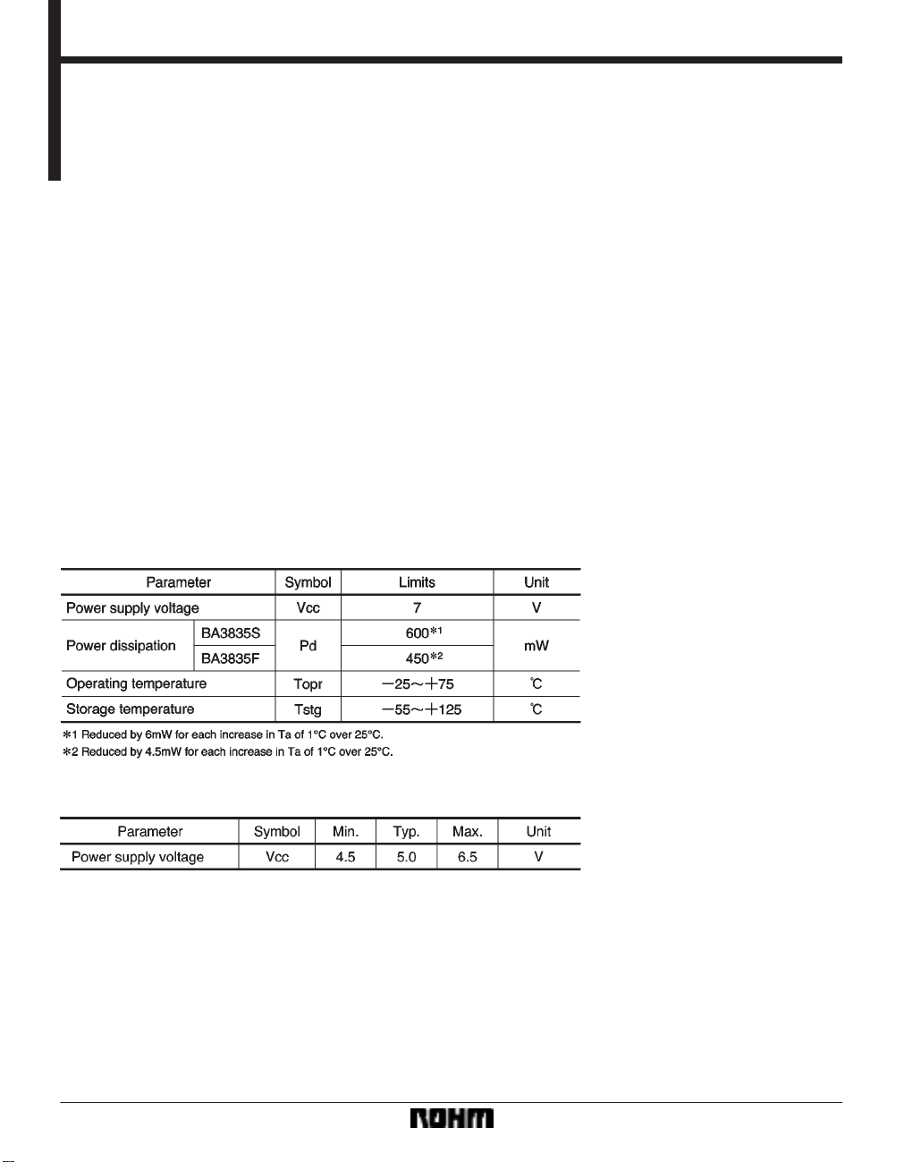
Absolute maximum ratings (Ta = 25C)
3) Discharge time constant circuit for each band is on
the chip.
4) Differential input amplifier rejects common-mode
noise.
5) Single 5V power supply.
Recommended operating conditions (Ta = 25C)
601
Audio ICs BA3835S / BA3835F
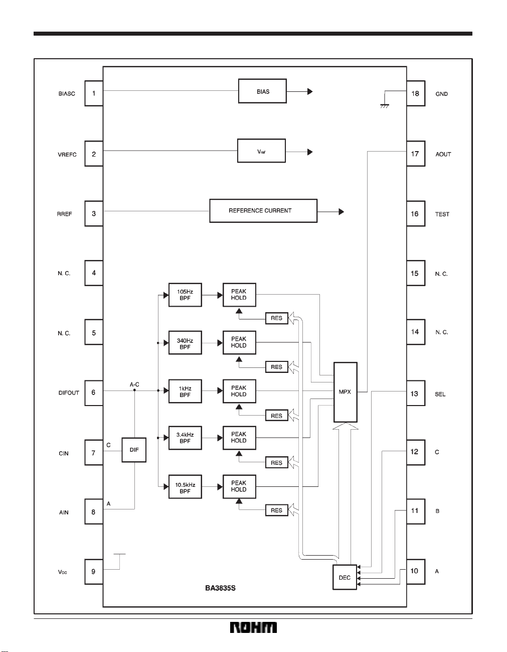
Block diagram 1 (BA3835S)
602
Audio ICs BA3835S / BA3835F
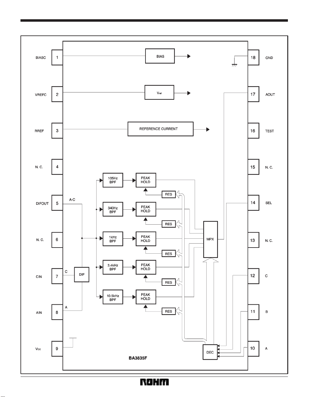
Block diagram 2 (BA3835F)
603

Audio ICs BA3835S / BA3835F
Electrical characteristics (unless otherwise noted, Ta = 25C, VCC = 5V, RL = 10MΩ, VAIN = 30dBV and
SEL = 1)
604

Audio ICs BA3835S / BA3835F
Measurement circuit (BA3835S)
605

Audio ICs BA3835S / BA3835F
Output select logic table
Timing chart
606

Audio ICs BA3835S / BA3835F
Application example (BA3835S)
607

Audio ICs BA3835S / BA3835F
Operation notes
(1) Frequency characteristics
The frequency characteristics of this IC are determined
by the resistor connected between the R
REF terminal and
GND. For the specification conditions, the value of this
resistor is 100kΩ. If it is necessary to set the frequency
characteristics accurately , use a variable resistor (note :
all bands will shift together).
And from this, the following condition is obtained :
R < 30kΩ
In this case, the “L” level voltage V
2 for the IC will
be :
V
2 < 0.75V
(2) Load characteristics
T o convert the bias sense output signal to the GND sense
signal, the IC performs a V / I conversion, and then an
I / V conversion using a 10kΩ resistor (typ.) for the output.
Therefore, if the load circuit connected to the A OUT pin
has a MOS structure there is no problem (eg. microprocessor input port), but if the connected circuit has a low
input impedance, it may cause the output level to drop.
(3) External resistor for the control pin
When using a common port for the output select control
and FL drive, you must add a diode and resistor as shown
in Fig. 4 to prevent the FL drive “L” voltage from destroying the IC.
In this case, the “L” voltage applied to the internal
comparator input terminal V
R1)R
1 = Vref
V
1)R2)R
R
1 is given by :
T o maintain a noise margin of at least 2.5V with respect to the comparator threshold level V
resentative values for V
ref, R1 and R2 are 1.5V , 20kΩ,
ref, the rep-
and 10kΩ respectively. This gives :
20kΩ)R
20kΩ)10kΩ)R
1.5V)0.25V<1.5V
(4) Recommended operating ranges
Provided that the IC is operated within the recommended
operating conditions and the recommended temperature
range, the basic circuit functions are guaranteed. Within
these ranges, ratings for electrical characteristics for
conditions other than those stipulated cannot be guaranteed, but the inherent function of the bandpass filter will
be maintained.
(5) Application circuit
Provided the recommended circuit constants are used,
the application circuit should function correctly. However ,
we recommend that you confirm the characteristics of the
circuits in actual use and pay due attention to the cautionary notes given below.
If you change the circuit constants, check both the static
and transient characteristics of the circuit, and allow sufficient margin to accommodate variations between both
ICs and external components. Note, also, that Rohm has
not been able to conduct a sufficient study into patent
rights.
608

Audio ICs BA3835S / BA3835F
(6) Output offset voltage
The relationship between the output offset voltage and
the output selection cycle (cycle time) for this IC is shown
in Fig.5. The maximum output offset voltage of 150mV
that is given in the electrical characteristics table is under
the condition that Ts = 200ms. When Ts is greater than
50ms, the graph of the output offset voltage is a straight
line at 150mV. When Ts is below 50ms, due to transient
characteristics of the peak hold circuit, the graph is a line
sloping downwards to the right. In other words, the shorter the cycle, the larger the output offset voltage.
Furthermore, the output offset voltage may shift due to
soldering or other temperature stresses from the surroundings. Therefore, when setting the spectral analyzer
light level, take into consideration the points given above
and make sure that it does not light by mistake during
quiescent periods. Use the chart below as a guide for
this, and, if necessary, leave even a larger margin.
Electrical characteristics curves
609

Audio ICs BA3835S / BA3835F
External dimensions (Units: mm)
610
 Loading...