


Audio ICs
Pre / power amplifier and motor
governor for 3V headphone stereos
BA3528AFP / BA3529AFP
The BA3528AFP and AB3529AFP have been developed for headphone stereos. They run off a 3V power supply , and
include dual pre- and power amplifiers, and a motor governor.
The preamplifiers are direct-coupled, and the power amplifiers use a fixed-gain NF circuit. An on-chip V
makes output coupling capacitors unnecessary , and the motor governor uses a bridge ratio system to minimize the external parts count and make reliable and compact designs possible.
Applications
3V portable stereo equipment
Features
1) All the functions required for headphone stereo units
on a single chip.
2) Preamplifier includes a mute amplifier.
3) Direct-coupled preamplifier.
4) No output coupling capacitors required for the power
amplifiers.
5) Power amplifiers do not require oscillation prevention
measures.
6) Power amplifier gain allows use of noise reduction
(BA3529AFP).
REF amplifier
Absolute maximum ratings (Ta = 25C)
Recommended operating conditions (Ta = 25C)
385

Audio ICs BA3528AFP / BA3529AFP
Block diagram
386
Audio ICs BA3528AFP / BA3529AFP
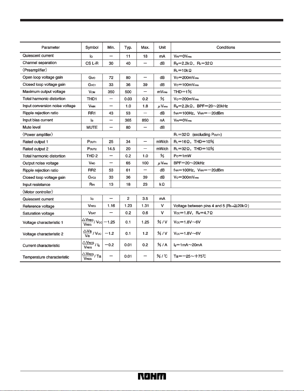
Electrical characteristics (unless otherwise noted, Ta = 25C, VCC = 3V, and f = 1kHz)
BA3528AFP
387

Audio ICs BA3528AFP / BA3529AFP
BA3529AFP
388

Audio ICs BA3528AFP / BA3529AFP
Measurement circuit
389

Audio ICs BA3528AFP / BA3529AFP
Circuit operation
(1) Preamplifier
In the preamplifier input stage the pin 22 bias is the input
and the negative feedback virtual earth, and the bias for
the input stage transistor is taken from pin 22 via the tape
head to allow direct coupling. Connect a 1000pF capacitor in parallel with the tape head to prevent high-frequency interference (see Fig. 2).
(4) Power amplifier
The power amplifier employs an NF circuit with fixed
gain. G
VC = 36dB (BA3528AFP) and GVC = 27dB
(BA3529AFP).
(2) Mute amplifier
Preamplifier output muting can be switched on and off.
The mute is off when the mute switch input (pin 1) is low
or open, and on when the mute switch input is high (tied
to V
CC via a resistor), see Fig. 3.
(3) Equalizer
The preamplifier is based on an NAB120µs NF-type
equalizer. It is possible to add a switching function for the
equalizer using the mute amplifier. Switching of the
equalizer constant is controlled by the voltage on pin 1
(low or high). Note, however, when this is done, preamplifier muting no longer operates (see Fig. 4).
For the input stage, the pin 22 bias point is the input and
the negative feedback virtual earth point, and the first
stage transistor bias is taken from pin 22. The built-in V
REF
amplifier uses the same bias point as its input, and its output voltage is about the same as DC output voltage from
the power amplifier. This becomes the virtual earth for the
headphones (see Fig. 5).
390

Audio ICs BA3528AFP / BA3529AFP
(5) Motor controller circuit
The motor controller circuit uses a resistance bridge to
maintain uniform motor speed regardless of changes in
supply voltage, ambient temperature and load torque.
Speed control is performed by a comparator and a stable
on-chip reference voltage (V
Application examples
REG = 1.23V). See Fig. 6.
391

Audio ICs BA3528AFP / BA3529AFP
392

Audio ICs BA3528AFP / BA3529AFP
Attached components
(1) Preamplifier
If the closed-loop voltage gain (G
VC) of the preamplifier
is below 30dB for a frequency of f = 1kHz, oscillation may
occur.
(2) Playback equalizer terminal (NAB)
The playback equalizer characteristics are determined
by the RC circuit connected between the output and NF
pins.
For the circuit in Fig. 9, with a closed-loop voltage gain
of GVC at an input frequency of 1 kHz, the relationships
between the values of the RC circuit components are as
follows:
C1 =
318010
120010
R
R2 = 2R110
–6
3
–GVC/20
the voltage difference between the pre-output and pin 22
will generate switching noise (a “pop” sound) when the
mute is switched on and off. To reduce the DC gain and
reduce this switching noise, we recommend that you
connect a resistor (R = 51 kΩ) as shown in Fig. 10. This
resistor reduces the gain of the circuit in the bass region
of the playback equalizer as shown in the graph in Fig.
11. By using dif ferent combinations of component values
for R
1 and C1, it is possible to compensate for this effect
in the low-frequency region as shown in the graph in Fig.
12.
The equalizer can be switched on and off using the mute
amplifier. If equalization for metal tape is added, determine R
3 as follows:
R
3 = 1.4 R1
(3) Pre-mute switching noise
If you use the mute amplifier for pre-muting,
393

Audio ICs BA3528AFP / BA3529AFP
(4) Mute amplifier output
To switch the mute amplifier on and off, switch the
constant-current supply for the mute amplifier off and on
by switching the voltage on pin 1 (Pre-mute SW) high or
low. When the mute is switched on, the mute amplifier
output goes open circuit and the output voltage is unstable resulting in the generation of an audible “pop” sound.
T o prevent this, bias pin 22 through the volume control as
shown in Fig. 13.
In applications that use a directly connected output coupling capacitor, connect a resister as shown in the circuit
diagram in Fig. 14 to reduce the pre-mute switching noise
described in (3) above.
(5) Preventing oscillation
Connect a capacitor of approximately 1000pF between
the preamplifier input and pin 22 to prevent oscillation,
and as a countermeasure against strong electric fields.
This capacitor can also be used for treble-region compensation. In this case, decide on a value for it based on
the relationship with the impedance of the magnetic head
(see Fig. 15).
When countermeasures against strong electric fields for
the power amplifiers are required, connect bypass capacitors between each input pin and pin 22, and connect
choke coils in series with the output pins and the headphones. The component values should be about 330pF
for the bypass capacitors, and the 10µH for the choke
coils so that they do not effect the audible frequency
range.
Another effective measure is to connect a bypass capacitor of about 1000pF in parallel with the filter capacitor between pin 22 and ground (pin 21). Refer to the circuit diagram in Fig. 16.
394

Audio ICs BA3528AFP / BA3529AFP
(6) Motor speed setting
To control the motor speed, the stable built-in reference
voltage V
REG is divided across R4 and R5, and this voltage
is used as the speed control voltage. The balance conditions for the bridge circuit are as follows:
R1
1)
R2
R
R2
R
*Ra
3
3
Ia
R5
R4)R5
VREG
Ea =
)
(however, Ir tt Ia)
From this, the balance conditions for the load fluctuation
zero are:
Ra = 10 R1
Ea = 11
4)R5
R
R5
VREG
Operation notes
(1) Application circuits
Provided the recommended circuit constants are used,
the application circuits should function correctly. However, we recommend that you confirm the characteristics of
the circuits in actual use. If you change the circuit
constants, check both the static and transient characteristics of the circuit, and allow sufficient margin to accommodate variations between both ICs and external components.
(2) Recommended supply voltage
The values given in the electrical characteristics table are
guaranteed only for Ta = 25C, and V
CC = 3V. However,
as long as the IC is operated within the recommended
operating temperature and supply voltage ranges, the
general circuit functions are guaranteed to operate correctly, and there will not be significant changes in the
electrical characteristics.
However, if Ra t 10 R1, the amount of positive feedback increases, and the circuit will be unstable, so within
the operating temperature range, always make
R
a y 10 R1 (see Fig. 17).
(3) Power dissipation
The internal power dissipation of the IC is depends
strongly on the value of the load resistance and the supply voltage.
For this reason, when designing sets for mass production, pay due consideration to the power dissipation characteristics of the IC with respect to ambient temperature
and supply voltage (see Figs. 18 and 19). Note, that the
maximum allowed power dissipation is 1.7W at 25C,
and this decreases by 13.6mW for each increase in temperature of 1C over this.
(4) PCB layout
In certain cases, the external circuit wiring can induce oscillations in the IC or degrade circuit performance. To
avoid this, design the PCB wiring in such a way as to keep
external wiring as short as possible, and ensure that it
does not have common impedance.
395

Audio ICs BA3528AFP / BA3529AFP
Electrical characteristic curves
396

Audio ICs BA3528AFP / BA3529AFP
Application board patterns Application board component layout
397

Audio ICs BA3528AFP / BA3529AFP
External dimensions (Units: mm)
398
 Loading...