

]30[mA]
]10[V/µs]10[V/µs]
Operational Amplifiers / Comparators
High Speed with High Voltage
Operational Amplifiers
Datasheet
BA3472, BA3472R, BA3474, BA3474R
●General Description
General-purpose BA3472,BA3472R,BA3474,BA3474R
integrate two/four Independent Op-amps and phase
compensation capacitors on a single chip and have some
features of high-gain, and wide operating voltage range of
+3[V] to +36[V](single power supply). Especially,
characteristics are high slew rate (10[V/μs]) and high
Maximum frequency (4[MHz]).
●Features
Operable with a single power supply
Wide operating supply voltage
Standard Op-Amp. Pin-assignments
Internal phase compensation
High open loop voltage gain
Internal ESD protection
Operable low input voltage around GND level
Wide output voltage range
●Packages (Typ.) (Typ.) (Max.)
MSOP8 2.90mm x 4.00mm x 0.90mm
SSOP-B8 3.00mm x 6.40mm x 1.35mm
SSOP-B14 5.00mm x 6.40mm x 1.35mm
SOP8 5.00mm x 6.20mm x 1.71mm
SOP14 8.70mm x 6.20mm x 1.71mm
●Selection Guide
●Key Specifications
Wide Operating Supply Voltage:
Single supply +3.0[V] to +36.0[V]
Dual supply ±1.5[V] to ±18.0[V]
Wide Temperature Range:
BA3474F -40[°C] to +75[°C]
BA3472F BA3472FV
BA3472FVM BA3474FV -40[°C] to +85[°C]
BA3472RFVM
BA3474RFV -40[°C] to +105[°C]
Low Input Offset Current: 6[nA] (Typ.)
Low Input Bias Current: 100[nA] (Typ.)
Wide Output Voltage Range:
VEE+0.3[V]-VCC-1.0[V](Typ.)
with VCC-VEE=30[V]
High Slew Rate: 10[V/µs]
Maximum Frequency: 4[MHz]
Human Body Model (HBM): ±5000[V] (Typ.)
Operation guaranteed
Output Current
Source/Sink
High Speed
○Product structure:Silicon monolithic integrated circuit ○This product is not designed protection against radioactive rays.
www.rohm.com TSZ02201-0RAR0G200100-1-2
© 2012 ROHM Co., Ltd. All rights reserved.
TSZ22111・14・001
Dual 30[mA]/ 30[mA
Quad
/ 30[mA
Slew Rate
1/39
+75[°C]
BA3474F
+85[°C]
BA3472F
BA3472FV
BA3472FVM
BA3474FV BA3474RFV
27.FEB.2012 Rev.001
+105[°C]
BA3472RFVM

A
BA3472, BA3472R, BA3474, BA3474R
●Pin Configuration(TOP VIEW)
OUT1
18
CH1
27
-IN1
+IN1
VEE
- +
36
CH2
+ -
45
SOP8
B
3472F BA3472FV
SSOP-B8
BA3472FVM
BA3472RFVM
●Ordering Information
VCC
OUT2
-IN2
+IN2
MSOP8
1
OUT1
-IN1
213
CH1
+IN1
VCC
+IN2
-IN2
OUT2
BA3474F
- +
312
4
5
- +
CH2
69
78
SOP14
BA3474FV
14
CH4
+ -
11
10
+ -
CH3
SSOP-B14
OUT4
-IN4
+IN4
VEE
+IN3
-IN3
OUT3
BA3474RFV
Datasheet
B A 3 4 7 x F x x - x x
Part Number
●Lineup
Topr
-40°C to +75°C 8.0mA
-40°C to +85°C
-40°C to +105°C
Supply
Current
(Typ.)
4.0mA
8.0mA SSOP-B14 Reel of 2500 BA3474FV-E2
4.0mA MSOP8 Reel of 3000 BA3472RFVM-TR
8.0mA SSOP-B14 Reel of 2500 BA3474RFV-E2
Package
F : SOP8
SOP14
FV : SSOP-B8
SSOP-B14
FVM : MSOP8
Slew Rate
(Typ.)
SOP14 Reel of 2500 BA3474F-E2
SOP8 Reel of 2500 BA3472F-E2
SSOP-B8 Reel of 2500 BA3472FV-E2
10.0V/µs
MSOP8 Reel of 3000 BA3472FVM-TR
Packaging and forming specification
E2: Embossed tape and reel
(SOP8/SOP14/SSOP-B8/SSOP-B14)
TR: Embossed tape and reel
(MSOP8)
Package
Orderable
Part Number
www.rohm.com TSZ02201-0RAR0G200100-1-2
© 2012 ROHM Co., Ltd. All rights reserved.
TSZ22111・15・001
2/39
27.FEB.2012 Rev.001
BA3472, BA3472R, BA3474, BA3474R
●Absolute Maximum Ratings (Ta=25[℃])
Ratings
Parameter Symbol
Supply Voltage
Differential Input Voltage
(*1)
Input Common-mode
Voltage Range
Operating Temperature Range
Storage Temperature Range
Maximum Junction Temperature
Note: Absolute maximum rating item indicates the condition which must not be exceeded.
Application if voltage in excess of absolute maximum rating or use out of absolute maximum rated temperature environment may cause
deterioration of characteristics.
(*1) The voltage difference between inverting input and non-inverting input is the differential input voltage.
Then input terminal voltage is set to more than VEE.
VCC-VEE +36 V
Vid 36 V
Vicm (VEE - 0.3) to VEE + 36 V
Topr
-40 to +85(SOP14:+75)
Tstg -55 to +150
Tjmax +150
BA3472
BA3474
BA3472R
BA3474R
-40 to +105 ℃
●Electrical Characteristics
○BA3472 (Unless otherwise specified VCC=+15[V], VEE=-15[V], Ta=25[℃])
Limits
Parameter Symbol
Temperature
range
Unit Condition BA3472F/FV/FVM
Min. Typ. Max.
Datasheet
Unit
℃
℃
- 1 10 mVVicm=0[V],VOUT=0[V]
Input Offset Voltage (*2) Vio 25℃
- 1.5 10
VCC=5[V],VEE=0[V],Vicm=0[V],
VOUT=VCC/2
Input Offset Current (*2) Iio 25℃ - 6 75 nA Vicm=0[V],VOUT=0[V]
Input Bias Current (*2) Ib 25℃ - 100 500 nA Vicm=0[V],VOUT=0[V]
Supply Current ICC 25℃ - 4 5.5 mA RL=∞
High Level Output Voltage VOH 25℃
3.7 4 -
13.7 14 - RL=10[kΩ]
VCC=5[V],RL=2[kΩ]
V
13.5 - - RL=2[kΩ]
- 0.1 0.3 V VCC=5[V],RL=2[kΩ]
Low Level Output Voltage VOL 25℃
- -14.7 -14.3 RL=10[kΩ]
- - -13.5 RL=2[kΩ]
Large Signal Voltage Gain AV 25℃ 80 100 - dB RL≧2[kΩ],VOUT=±10 [V]
Input Common-mode
Voltage Range
Vicm 25℃ 0 - VCC-2.0 V
VCC=5[V],VEE=0[V],
VOUT=VCC/2
Common-mode Rejection Ratio CMRR 25℃ 60 97 - dB Vicm=0[V],VOUT=0[V]
Power Supply Rejection Ratio PSRR 25℃ 60 97 - dB Vicm=0[V],VOUT=0[V]
VCC=5[V],VIN+=1[V],
Output Source Current (*3) IOH 25℃ 10 30 - mA
VIN-=0[V],VOUT=0[V]
Only 1ch is short circuit
VCC=5[V],VIN+=0[V],
Output Sink Current (*3) IOL 25℃ 20 30 - mA
VIN-=1[V],VOUT=5[V],
Only 1ch is short circuit
Maximum Frequency ft 25℃ - 4 - MHz -
Slew Rate SR 25℃ - 10 - V/μs
Av=1,Vin=-10 to +10[V],
RL=2[kΩ]
Channel Separation CS 25℃ - 120 - dB -
(*2) Absolute value
(*3) Under high temperatures, please consider the power dissipation when selecting the output current.
When the output terminal is continuously shorted the output current reduces the internal temperature by flushing.
www.rohm.com TSZ02201-0RAR0G200100-1-2
© 2012 ROHM Co., Ltd. All rights reserved.
TSZ22111・15・001
3/39
27.FEB.2012 Rev.001
BA3472, BA3472R, BA3474, BA3474R
○BA3472R (Unless otherwise specified VCC=+15[V], VEE=-15[V], Ta=25[℃])
Limits
Parameter
Symbol
Temperature
range
BA3472RFVM
Min. Typ. Max.
Unit
Datasheet
Condition
- 1 10 mVVicm=0[V],VOUT=0[V]
- 1.5 10
VCC=5[V],VEE=0[V],Vicm=0[V],
VOUT=VCC/2
Input Offset Voltage
Input Offset Current
Input Bias Current
(*4)
(*4)
Vio 25℃
(*4)
Iio 25℃ - 6 75 nA Vicm=0[V],VOUT=0[V]
Ib 25℃ - 100 500 nA Vicm=0[V],VOUT=0[V]
Supply Current ICC 25℃ - 4 5.5 mA RL=∞
High Level Output Voltage VOH 25℃
3.7 4 -
13.7 14 - RL=10[kΩ]
VCC=5[V],RL=2[kΩ]
V
13.5 - - RL=2[kΩ]
- 0.1 0.3 V VCC=5[V],RL=2[kΩ]
Low Level Output Voltage VOL 25℃
- -14.7 -14.3 RL=10[kΩ]
- - -13.5 RL=2[kΩ]
Large Signal Voltage Gain AV 25℃ 80 100 - dB RL≧2[kΩ],VOUT=±10 [V]
Input Common-mode
Voltage Range
Vicm 25℃ 0 - VCC-2.0 V
VCC=5[V],VEE=0[V],
VOUT=VCC/2
Common-mode Rejection Ratio CMRR 25℃ 60 97 - dB Vicm=0[V],VOUT=0[V]
Power Supply Rejection Ratio PSRR 25℃ 60 97 - dB Vicm=0[V],VOUT=0[V]
Output Source Current
(*5)
IOH 25℃ 10 30 - mA
VCC=5[V],VIN+=1[V],
VIN-=0[V], VOUT=0[V]
Only 1ch is short circuit
VCC=5[V],VIN+=0[V],
VIN-=1[V], VOUT=5[V]
Output Sink Current
(*5)
IOL 25℃ 20 30 - mA
Only 1ch is short circuit
Maximum Frequency ft 25℃ - 4 - MHz -
Slew Rate SR 25℃ - 10 - V/μs
Av=1,Vin=-10 to +10[V],
RL=2[kΩ]
Channel Separation CS 25℃ - 120 - dB -
(*4) Absolute value
(*5) Under high temperatures, please consider the power dissipation when selecting the output current.
When the output terminal is continuously shorted the output current reduces the internal temperature by flushing.
www.rohm.com TSZ02201-0RAR0G200100-1-2
© 2012 ROHM Co., Ltd. All rights reserved.
TSZ22111・15・001
4/39
27.FEB.2012 Rev.001

BA3472, BA3472R, BA3474, BA3474R
○BA3474 (Unless otherwise specified VCC=+15[V], VEE=-15[V], Ta=25[℃])
Limits
Parameter Symbol
Temperature
range
Min. Typ. Max.
Datasheet
Unit Condition BA3474F/FV
- 1 10 mVVicm=0[V],VOUT=0[V]
- 1.5 10
VCC=5[V],VEE=0[V], Vicm=0[V]
VOUT=VCC/2
Input Offset Voltage
Input Offset Current
Input Bias Current
(*6)
Vio 25℃
(*6)
Iio 25℃ - 6 75 nA Vicm=0[V],VOUT=0[V]
(*6)
Ib 25℃ - 100 500 nA Vicm=0[V],VOUT=0[V]
Supply Current ICC 25℃ - 8 11 mA RL=∞
High Level Output Voltage VOH 25℃
3.7 4 -
13.7 14 - RL=10[kΩ]
VCC=5[V],RL=2[kΩ]
V
13.5 - - RL=2[kΩ]
- 0.1 0.3 V VCC=5[V],RL=2[kΩ]
- -14.7 -14.3 RL=10[kΩ]
Low Level Output Voltage
VOL 25℃
- - -13.5 RL=2[kΩ]
Large Signal Voltage Gain AV 25℃ 80 100 - dB RL≧2[kΩ], VOUT=±10 [V]
Input Common-mode Voltage
Range
Vicm 25℃ 0 - VCC-2.0 V
VCC=5[V],VEE=0[V],
VOUT=VCC/2
Common-mode Rejection Ratio CMRR 25℃ 60 97 - dB Vicm=0[V],VOUT=0[V]
Power Supply Rejection Ratio PSRR 25℃ 60 97 - dB Vicm=0[V],VOUT=0[V]
Output Source Current
(*7)
IOH 25℃ 10 30 - mA
VCC=5[V],VIN+=1[V],
VIN-=0[V], VOUT=0[V]
Only 1ch is short circuit
VCC=5[V],VIN+=0[V],
VIN-=1[V], VOUT=5[V]
Output Sink Current
(*7)
IOL 25℃ 20 30 - mA
Only 1ch is short circuit
Maximum Frequency ft 25℃ - 4 - MHz -
Slew Rate SR 25℃ - 10 - V/μs
Av=1,Vin=-10 to +10[V],
RL=2[kΩ]
Channel Separation CS 25℃ - 120 - dB -
(*6) Absolute value
(*7) Under high temperatures, please consider the power dissipation when selecting the output current.
When the output terminal is continuously shorted the output current reduces the internal temperature by flushing.
www.rohm.com TSZ02201-0RAR0G200100-1-2
© 2012 ROHM Co., Ltd. All rights reserved.
TSZ22111・15・001
5/39
27.FEB.2012 Rev.001

BA3472, BA3472R, BA3474, BA3474R
○BA3474R (Unless otherwise specified VCC=+15[V], VEE=-15[V], Ta=25[℃])
Limits
Parameter Symbol
Temperature
range
Min. Typ. Max.
Datasheet
Unit Condition BA3474RFV
(*8)
(*8)
(*8)
Input Offset Voltage
Input Offset Current
Input Bias Current
Supply Current
High Level Output Voltage
Low Level Output Voltage
Large Signal Voltage Gain
Input Common-mode Voltage
Range
Common-mode Rejection Ratio
Power Supply Rejection Ratio
(*9)
(*9)
Output Source Current
Output Sink Current
Maximum Frequency
- 1 10
- 1.5 10
Vio
25℃
Iio 25℃ - 6 75 nA
Ib
25℃
- 100 500 nA
ICC 25℃ - 8 11 mA
3.7 4 -
VOH
25℃
13.7 14 -
13.5 - -
- 0.1 0.3
VOL
25℃
- -14.7 -14.3
- - -13.5
AV
25℃
80 100 - dB
Vicm 25℃ 0 - VCC-2.0 V
CMRR
25℃
60 97 - dB
PSRR 25℃ 60 97 - dB
Vicm=0[V],VOUT=0[V]
mV
VCC=5[V],VEE=0[V],Vicm=0[V],
VOUT=VCC/2
Vicm=0[V],VOUT=0[V]
Vicm=0[V],VOUT=0[V]
RL=∞
VCC=5[V],RL=2[kΩ]
RL=10[kΩ]
V
RL=2[kΩ]
VCC=5[V],RL=2[kΩ]
RL=10[kΩ]
V
RL=2[kΩ]
RL≧2[kΩ],VOUT=±10 [V]
VCC=5[V],VEE=0[V],
VOUT=VCC/2
Vicm=0[V],VOUT=0[V]
Vicm=0[V],VOUT=0[V]
VCC=5[V],VIN+=1[V],
IOH
25℃
10 30 - mA
VIN-=0[V],VOUT=0[V],
Only 1ch is short circuit
VCC=5[V],VIN+=0[V],
IOL
25℃
20 30 - mA
VIN-=1[V],VOUT=5[V],
Only 1ch is short circuit
ft 25℃ - 4 - MHz
-
Slew Rate
Channel Separation
(*8) Absolute value
(*9) Under high temperatures, please consider the power dissipation when selecting the output current.
When the output terminal is continuously shorted the output current reduces the internal temperature by flushing.
SR
CS 25℃ - 120 - dB
25℃
- 10 - V/μs
Av=1,Vin=-10 to +10[V],RL=2[kΩ]
-
www.rohm.com TSZ02201-0RAR0G200100-1-2
© 2012 ROHM Co., Ltd. All rights reserved.
TSZ22111・15・001
6/39
27.FEB.2012 Rev.001

BA3472, BA3472R, BA3474, BA3474R
Description of Electrical Characteristics
Described below are descriptions of the relevant electrical terms
Please note that item names, symbols and their meanings may differ from those on another manufacturer’s documents.
1. Absolute maximum ratings
The absolute maximum ratings are values that should never be exceeded, since doing so may result in deterioration of
electrical characteristics or damage to the part itself as well as peripheral components.
1.1 Power supply voltage (VCC-VEE)
Expresses the maximum voltage that can be supplied between the positive and negative supply terminals without
causing deterioration of the electrical characteristics or destruction of the internal circuitry.
1.2 Differential input voltage (Vid)
Indicates the maximum voltage that can be supplied between the non-inverting and inverting terminals without
damaging the IC.
1.3 Input common-mode voltage range (Vicm)
Signifies the maximum voltage that can be supplied to non-inverting and inverting terminals without causing
deterioration of the characteristics or damage to the IC itself. Normal operation is not guaranteed within the
common-mode voltage range of the maximum ratings – use within the input common-mode voltage range of the
electric characteristics instead.
1.4 Power dissipation (Pd)
Indicates the power that can be consumed by a particular mounted board at ambient temperature (25℃). For
packaged products, Pd is determined by the maximum junction temperature and the thermal resistance.
2. Electrical characteristics
2.1 Input offset voltage (Vio)
Signifies the voltage difference between the non-inverting and inverting terminals. It can be thought of as the input
voltage difference required for setting the output voltage to 0 V.
2.2 Input offset current (Iio)
Indicates the difference of input bias current between the non-inverting and inverting terminals.
2.3 Input bias current (Ib)
Denotes the current that flows into or out of the input terminal, it is defined by the average of the input bias current at
the non-inverting terminal and the input bias current at the inverting terminal.
2.4 Circuit current (ICC)
Indicates the current of the IC itself that flows under specified conditions and during no-load steady state.
2.5
maximum output voltage (VOM)
Indicates the voltage range that can be output by the IC under specified load condition. It is typically divided into
high-level output voltage and low-level output voltage.
2.6 Large signal voltage gain (AV)
The amplifying rate (gain) of the output voltage against the voltage difference between non-inverting and inverting
terminals, it is (normally) the amplifying rate (gain) with respect to DC voltage.
AV = (output voltage fluctuation) / (input offset fluctuation)
2.7 Input common-mode voltage range (Vicm)
Indicates the input voltage range under which the IC operates normally.
2.8 Common-mode rejection ratio (CMRR)
Signifies the ratio of fluctuation of the input offset voltage when the in-phase input voltage is changed (DC fluctuation).
CMRR = (change in input common-mode voltage) / (input offset fluctuation)
2.9 Power supply rejection ratio (PSRR)
Denotes the ratio of fluctuation of the input offset voltage when supply voltage is changed (DC fluctuation).
SVR = (change in power supply voltage) / (input offset fluctuation)
2.10 Channel separation (CS)
Expresses the amount of fluctuation of the input offset voltage or output voltage with respect to the change in the
output voltage of a driven channel.
2.11 Slew rate (SR)
Indicates the time fluctuation ratio of the output voltage when an input step signal is supplied.
2.12 Maximum frequency (ft)
Indicates a frequency where the voltage gain of Op-Amp is 1.
2.13 Total harmonic distortion + Noise (THD+N)
Indicates the fluctuation of input offset voltage or that of output voltage with reference to the change of output voltage
of driven channel.
2.14 Input referred noise voltage (Vn)
Indicates a noise voltage generated inside the operational amplifier equivalent by ideal voltage source connected in
series with input terminal.
Datasheet
www.rohm.com TSZ02201-0RAR0G200100-1-2
© 2012 ROHM Co., Ltd. All rights reserved.
TSZ22111・15・001
7/39
27.FEB.2012 Rev.001

V
BA3472, BA3472R, BA3474, BA3474R
●Circuit Diagram
VCC
VIN-
IN+
VEE
Fig.1 Schematic diagram (one channel only)
Datasheet
VOUT
www.rohm.com TSZ02201-0RAR0G200100-1-2
© 2012 ROHM Co., Ltd. All rights reserved.
TSZ22111・15・001
8/39
27.FEB.2012 Rev.001
BA3472, BA3472R, BA3474, BA3474R
●Typical Performance Curves
BA3472
Supply Current - Ambient Temperature
Fig.2
Derating Curve
Fig.4
Datasheet
Fig.3
Supply Current - Supply Voltage
Fig.5
High level Output Voltage - Supply Voltage
(RL=10[kΩ])
www.rohm.com TSZ02201-0RAR0G200100-1-2
© 2012 ROHM Co., Ltd. All rights reserved.
TSZ22111・15・001
9/39
27.FEB.2012 Rev.001
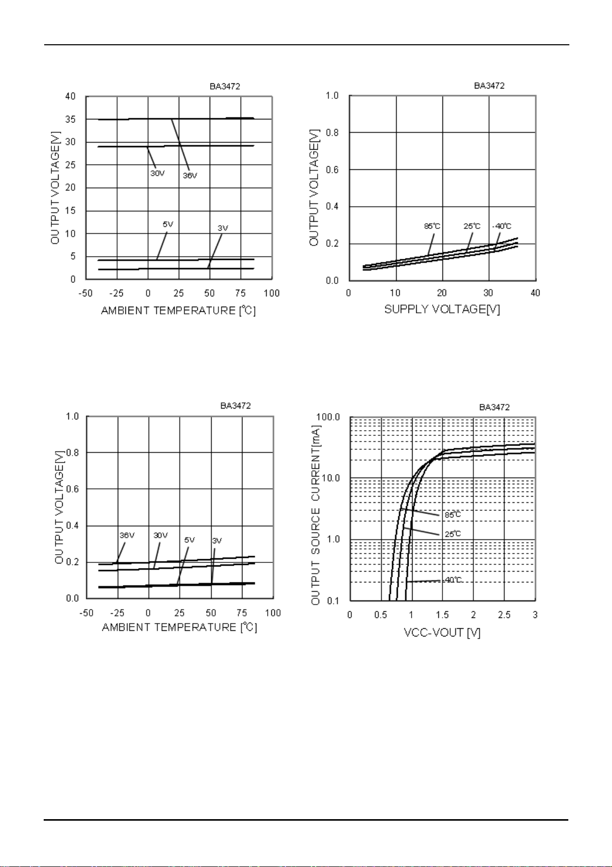
BA3472, BA3472R, BA3474, BA3474R
High level Output Voltage
- Ambient Temperature
Low level Output Voltage
- Ambient Temperature
Fig.6
(RL=10[kΩ])
Fig.8
(RL=10[kΩ])
Datasheet
Fig.7
Low level Output Voltage
- Supply Voltage
(RL=10[kΩ])
Fig.9
Output Source Current - (VCC-VOUT)
(VCC/VEE=5[V]/0[V])
www.rohm.com TSZ02201-0RAR0G200100-1-2
© 2012 ROHM Co., Ltd. All rights reserved.
TSZ22111・15・001
10/39
27.FEB.2012 Rev.001

BA3472, BA3472R, BA3474, BA3474R
(*)The data above is ability value of sample, it is not guaranteed
Output Source Current - (VOUT-VEE)
(VCC/VEE=5[V]/0[V])
Input Offset Voltage - Supply voltage
Fig.10
Fig.12
Datasheet
Fig.11
Input Offset Voltage
- Common Model Input Voltage
(VCC/VEE=15[V]/-15[V])
Fig.13
Input Offset Voltage - Ambient Temperature
www.rohm.com TSZ02201-0RAR0G200100-1-2
© 2012 ROHM Co., Ltd. All rights reserved.
TSZ22111・15・001
11/3 9
27.FEB.2012 Rev.001
BA3472, BA3472R, BA3474, BA3474R
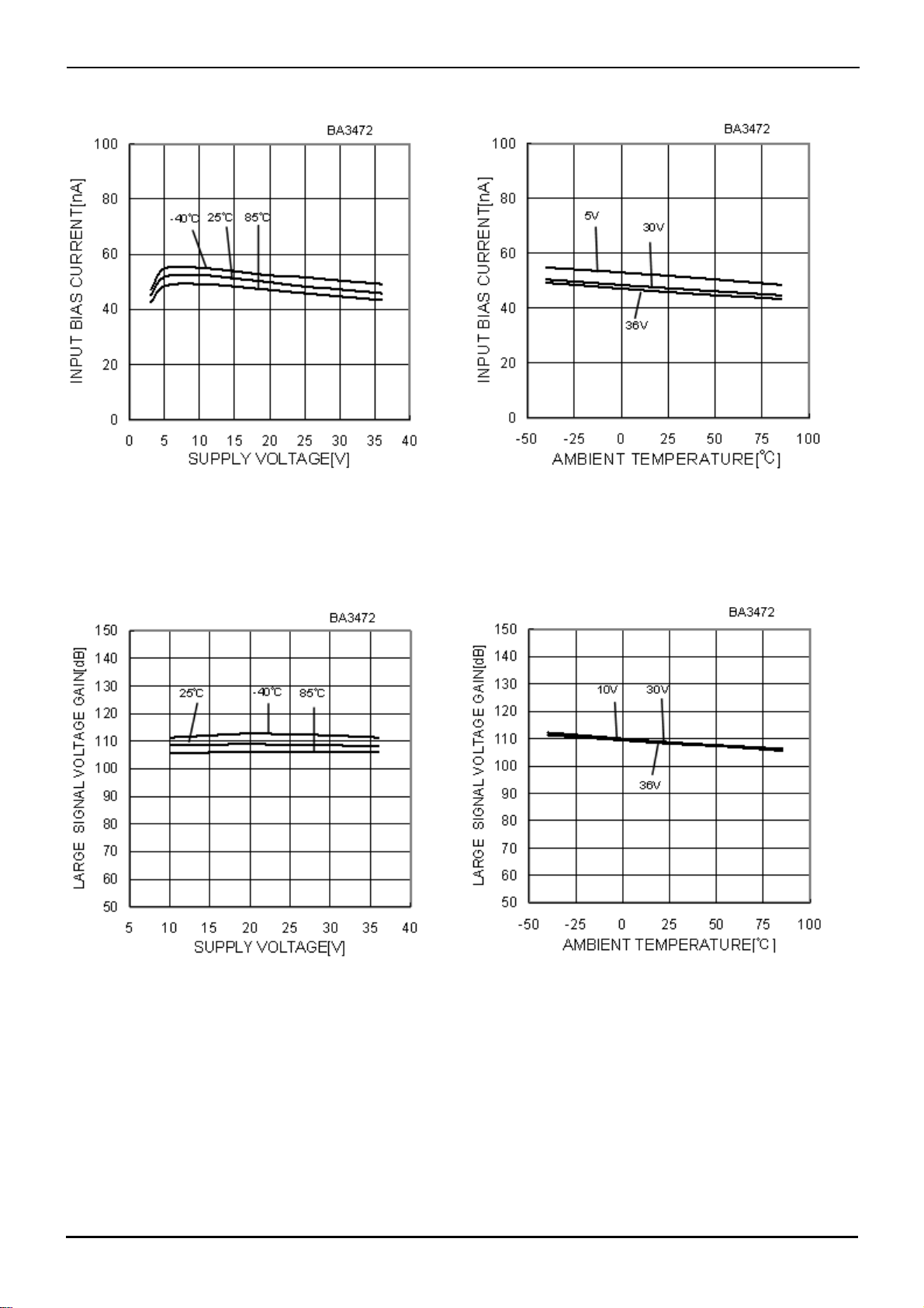
Input Bias Current - Supply voltage
Large Signal Voltage Gain
Fig.14
Fig.16
-Supply Voltage
Datasheet
Fig.15
Input Bias Current - Ambient Temperature
Fig.17
Large Signal Voltage Gain
-Ambient Temperature
www.rohm.com TSZ02201-0RAR0G200100-1-2
© 2012 ROHM Co., Ltd. All rights reserved.
TSZ22111・15・001
12/39
27.FEB.2012 Rev.001

BA3472, BA3472R, BA3474, BA3474R
Common Mode Rejection Ratio
Slew Rate L-H - Supply Voltage
Fig.18
-Supply Voltage
Fig.20
(RL=10[kΩ])
Datasheet
Fig.19
Common Mode Rejection Ratio
-Ambient Temperature
Fig.21
Slew Rate L-H - Ambient Temperature
(RL=10[kΩ])
www.rohm.com TSZ02201-0RAR0G200100-1-2
© 2012 ROHM Co., Ltd. All rights reserved.
TSZ22111・15・001
13/39
27.FEB.2012 Rev.001

BA3472, BA3472R, BA3474, BA3474R
(*)The data above is ability value of sample, it is not guaranteed
Voltage Gain - Frequency
(VCC=7.5[V]/-7.5[V], Av=40[dB],
RL=2[kΩ],CL=100[pF],Ta=25[℃])
Input / Output Voltage - Time
(VCC/VEE=15[V]/-15[V], Av=0[dB],
RL=2[kΩ], CL=100[pF], Ta=25[℃])
Fig.22
Fig.24
Datasheet
Fig.23
Input / Output Voltage - Time
(VCC/VEE=15[V]/-15[V], Av=0[dB],
RL=2[kΩ],CL=100[pF],Ta=25[℃])
www.rohm.com TSZ02201-0RAR0G200100-1-2
© 2012 ROHM Co., Ltd. All rights reserved.
TSZ22111・15・001
14/39
27.FEB.2012 Rev.001

BA3472, BA3472R, BA3474, BA3474R
BA3474
Supply Current - Ambient Temperature
Fig.25
Derating Curve
Fig.27
Datasheet
Fig.26
Supply Current - Supply Voltage
Fig.28
High level Output Voltage
- Supply Voltage
(RL=10[kΩ])
www.rohm.com TSZ02201-0RAR0G200100-1-2
© 2012 ROHM Co., Ltd. All rights reserved.
TSZ22111・15・001
15/39
27.FEB.2012 Rev.001

BA3472, BA3472R, BA3474, BA3474R
High level Output Voltage
- Ambient Temperature
Low level Output Voltage
- Ambient Temperature
Fig.29
(RL=10[kΩ])
Fig.31
(RL=10[kΩ])
Datasheet
Fig.30
Low level Output Voltage
- Supply Voltage
(RL=10[kΩ])
Fig.32
Output Source Current - (VCC-VOUT)
(VCC/VEE=5[V]/0[V])
www.rohm.com TSZ02201-0RAR0G200100-1-2
© 2012 ROHM Co., Ltd. All rights reserved.
TSZ22111・15・001
16/39
27.FEB.2012 Rev.001

BA3472, BA3472R, BA3474, BA3474R
(*)The data above is ability value of sample, it is not guaranteed
Output Source Current - (VOUT-VEE)
(VCC/VEE=5[V]/0[V])
Input Offset Voltage - Supply voltage
Fig.33
Fig.35
Datasheet
Fig.34
Input Offset Voltage
- Common Model Input Voltage
(VCC/VEE=15[V]/-15[V])
Fig.36
Input Offset Voltage -Ambient Temperature
www.rohm.com TSZ02201-0RAR0G200100-1-2
© 2012 ROHM Co., Ltd. All rights reserved.
TSZ22111・15・001
17/39
27.FEB.2012 Rev.001

BA3472, BA3472R, BA3474, BA3474R
Input Bias Current - Supply voltage
Large Signal Voltage Gain
Fig.37
Fig.39
-Supply Voltage
Datasheet
Fig.38
Input Bias Current - Ambient Temperature
Fig.40
Large Signal Voltage Gain
-Ambient Temperature
www.rohm.com TSZ02201-0RAR0G200100-1-2
© 2012 ROHM Co., Ltd. All rights reserved.
TSZ22111・15・001
18/39
27.FEB.2012 Rev.001

BA3472, BA3472R, BA3474, BA3474R
Common Mode Rejection Ratio
Slew Rate L-H - Supply Voltage
Fig.41
-Supply Voltage
Fig.43
(RL=10[kΩ])
Datasheet
Fig.42
Common Mode Rejection Ratio
-Ambient Temperature
Fig.44
Slew Rate L-H - Ambient Temperature
(RL=10[kΩ])
www.rohm.com TSZ02201-0RAR0G200100-1-2
© 2012 ROHM Co., Ltd. All rights reserved.
TSZ22111・15・001
19/39
27.FEB.2012 Rev.001

BA3472, BA3472R, BA3474, BA3474R
(*)The data above is ability value of sample, it is not guaranteed.
Voltage Gain - Frequency
(VCC=7.5[V]/-7.5[V], Av=40[dB],
RL=2[kΩ],CL=100[pF],Ta=25[℃])
Input / Output Voltage - Time
(VCC/VEE=15[V]/-15[V], Av=0[dB],
RL=2[kΩ],CL=100[pF],Ta=25[℃])
Fig.45
Fig.47
Datasheet
Fig.46
Input / Output Voltage - Time
(VCC/VEE=15[V]/-15[V], Av=0[dB],
RL=2[kΩ],CL=100[pF],Ta=25[℃])
www.rohm.com TSZ02201-0RAR0G200100-1-2
© 2012 ROHM Co., Ltd. All rights reserved.
TSZ22111・15・001
20/39
27.FEB.2012 Rev.001

BA3472, BA3472R, BA3474, BA3474R
BA3472R
Supply Current - Ambient
Fig.48
Derating Curve
Fig.50
Temperature
Datasheet
Fig.49
Supply Current - Supply Voltage
Fig.51
High level Output Voltage
- Supply Voltage
(RL=10[kΩ])
www.rohm.com TSZ02201-0RAR0G200100-1-2
© 2012 ROHM Co., Ltd. All rights reserved.
TSZ22111・15・001
21/39
27.FEB.2012 Rev.001

BA3472, BA3472R, BA3474, BA3474R
High level Output Voltage
- Ambient Temperature
Low level Output Voltage
- Ambient Temperature
Fig.52
(RL=10[kΩ])
Fig.54
(RL=10[kΩ])
Datasheet
Fig.53
Low level Output Voltage
- Supply Voltage
(RL=10[kΩ])
Fig.55
Output Source Current - (VCC-VOUT)
(VCC/VEE=5[V]/0[V])
www.rohm.com TSZ02201-0RAR0G200100-1-2
© 2012 ROHM Co., Ltd. All rights reserved.
TSZ22111・15・001
22/39
27.FEB.2012 Rev.001

(
BA3472, BA3472R, BA3474, BA3474R
(*)The data above is ability value of sample, it is not guaranteed.
Output Source Current -
Input Offset Voltage - Supply voltage
Fig.56
(VOUT-VEE)
VCC/VEE=5[V]/0[V])
Fig.58
Datasheet
Fig.57
Input Offset Voltage
- Common Model Input Voltage
(VCC/VEE=15[V]/-15[V])
Fig.59
Input Offset Voltage - Ambient
Temperature
www.rohm.com TSZ02201-0RAR0G200100-1-2
© 2012 ROHM Co., Ltd. All rights reserved.
TSZ22111・15・001
23/39
27.FEB.2012 Rev.001

BA3472, BA3472R, BA3474, BA3474R
Input Bias Current - Supply
Large Signal Voltage Gain
Fig.60
voltage
Fig.62
-Supply Voltage
Datasheet
Fig.61
Input Bias Current - Ambient
Temperature
Fig.63
Large Signal Voltage Gain
-Ambient Temperature
www.rohm.com TSZ02201-0RAR0G200100-1-2
© 2012 ROHM Co., Ltd. All rights reserved.
TSZ22111・15・001
24/39
27.FEB.2012 Rev.001

BA3472, BA3472R, BA3474, BA3474R
Datasheet
Fig.64
Common Mode Rejection Ratio
-Supply Voltage
Common Mode Rejection Ratio
Fig.65
-Ambient Temperature
Slew Rate L-H - Supply Voltage
www.rohm.com TSZ02201-0RAR0G200100-1-2
© 2012 ROHM Co., Ltd. All rights reserved.
TSZ22111・15・001
Fig.66
(RL=10[kΩ])
25/39
Slew Rate L-H - Ambient Temperature
Fig.67
(RL=10[kΩ])
27.FEB.2012 Rev.001

BA3472, BA3472R, BA3474, BA3474R
(*) The data above is ability value of sample, it is not guaranteed.
Voltage Gain - Frequency
(VCC=7.5[V]/-7.5[V], Av=40[dB],
RL=2[kΩ],CL=100[pF],Ta=25[℃])
Input / Output Voltage - Time
(VCC/VEE=15[V]/-15[V], Av=0[dB],
RL=2[kΩ],CL=100[pF],Ta=25[℃])
Fig.68
Fig.70
Datasheet
Fig.69
Input / Output Voltage - Time
(VCC/VEE=15[V]/-15[V], Av=0[dB],
RL=2[kΩ],CL=100[pF],Ta=25[℃])
www.rohm.com TSZ02201-0RAR0G200100-1-2
© 2012 ROHM Co., Ltd. All rights reserved.
TSZ22111・15・001
26/39
27.FEB.2012 Rev.001

BA3472, BA3472R, BA3474, BA3474R
BA3474R
Supply Current - Ambient Temperature
Fig.71
Derating Curve
Fig.73
Datasheet
Fig.72
Supply Current - Supply Voltage
Fig.74
High level Output Voltage
- Supply Voltage
(RL=10[kΩ])
www.rohm.com TSZ02201-0RAR0G200100-1-2
© 2012 ROHM Co., Ltd. All rights reserved.
TSZ22111・15・001
27/39
27.FEB.2012 Rev.001

BA3472, BA3472R, BA3474, BA3474R
High level Output Voltage
- Ambient Temperature
Low level Output Voltage
- Ambient Temperature
Fig.75
(RL=10[kΩ])
Fig.77
(RL=10[kΩ])
Datasheet
Fig.76
Low level Output Voltage
- Supply Voltage
(RL=10[kΩ])
Fig.78
Output Source Current - (VCC-VOUT)
(VCC/VEE=5[V]/0[V])
www.rohm.com TSZ02201-0RAR0G200100-1-2
© 2012 ROHM Co., Ltd. All rights reserved.
TSZ22111・15・001
28/39
27.FEB.2012 Rev.001

BA3472, BA3472R, BA3474, BA3474R
(*)The data above is ability value of sample, it is not guaranteed
Output Source Current - (VOUT-VEE)
Input Offset Voltage - Supply voltage
Fig.79
(VCC/VEE=5[V]/0[V])
Fig.81
Datasheet
Fig.80
Input Offset Voltage
- Common Model Input Voltage
(VCC/VEE=15[V]/-15[V])
Fig.82
Input Offset Voltage -Ambient Temperature
www.rohm.com TSZ02201-0RAR0G200100-1-2
© 2012 ROHM Co., Ltd. All rights reserved.
TSZ22111・15・001
29/39
27.FEB.2012 Rev.001

BA3472, BA3472R, BA3474, BA3474R
Input Bias Current - Supply voltage
Fig.83
Datasheet
Fig.84
Input Bias Current - Ambient Temperature
Fig.85
Large Signal Voltage Gain
-Supply Voltage
www.rohm.com TSZ02201-0RAR0G200100-1-2
© 2012 ROHM Co., Ltd. All rights reserved.
TSZ22111・15・001
30/39
Large Signal Voltage Gain
-Ambient Temperature
Fig.86
27.FEB.2012 Rev.001

BA3472, BA3472R, BA3474, BA3474R
Common Mode Rejection Ratio
Fig.87
-Supply Voltage
Datasheet
Fig.88
Common Mode Rejection Ratio
-Ambient Temperature
Fig.89
Slew Rate L-H - Supply Voltage
(RL=10[kΩ])
www.rohm.com TSZ02201-0RAR0G200100-1-2
© 2012 ROHM Co., Ltd. All rights reserved.
TSZ22111・15・001
31/39
Slew Rate L-H - Ambient Temperature
Fig.90
(RL=10[kΩ])
27.FEB.2012 Rev.001

BA3472, BA3472R, BA3474, BA3474R
(*)The data above is ability value of sample, it is not guaranteed
Voltage Gain - Frequency
(VCC=7.5[V]/-7.5[V], Av=40[dB],
RL=2[kΩ],CL=100[pF],Ta=25[℃])
Input / Output Voltage - Time
(VCC/VEE=15[V]/-15[V], Av=0[dB],
RL=2[kΩ],CL=100[pF],Ta=25[℃])
Fig.91
Fig.93
Datasheet
Fig.92
Input / Output Voltage - Time
(VCC/VEE=15[V]/-15[V], Av=0[dB],
RL=2[kΩ],CL=100[pF],Ta=25[℃])
www.rohm.com TSZ02201-0RAR0G200100-1-2
© 2012 ROHM Co., Ltd. All rights reserved.
TSZ22111・15・001
32/39
27.FEB.2012 Rev.001

A
BA3472, BA3472R, BA3474, BA3474R
●Application Information
Test circuit 1 NULL method
Parameter VF S1 S2 S3 VCC VEE EK Vicm Calculation
Datasheet
VCC, VEE, EK, Vicm Unit : [V]
Input Offset Voltage
Input Offset Current
Input Bias Current
Large Signal Voltage Gain
Common-mode Rejection Ratio
(Input Common-mode Voltage Range)
Power Supply Rejection Ratio
-Calculation-
1. Input Offset Voltage (Vio)
Vio =
| VF1 |
1 + Rf / Rs
[V]
2. Input Offset Current (Iio)
| VF2-VF1 |
Iio =
Ri ×(1 + Rf / Rs)
[A]
3. Input Bias Current (Ib)
| VF4-VF3 |
Ib =
2×Ri× (1 + Rf / Rs)
4. Large Signal Voltage Gain (Av)
v = 20×Log
EK×(1+Rf /Rs)
Δ
|VF5-VF6|
5. Common-mode Rejection Ratio (CMRR)
CMRR = 20×Log
Vicm×(1+Rf /Rs)
Δ
|VF8-VF7|
6. Power Supply Rejection Ratio (PSRR)
PSRR = 20×Log
Vcc×(1+Rf/Rs)
Δ
|VF10-VF9|
Test circuit2 switch condition
[A]
VF1 ON ON OFF 15 -15 0 0 1
VF2 OFF OFF OFF 15 -15 0 0 2
VF3 OFF ON
VF4 ON OFF
VF5
VF6 15 -15 -10 0
VF7
VF8 15 -15 0 13
VF9
VF10 18 -18 0 0
[dB]
[dB]
[dB]
ON ON ON
ON ON OFF
ON ON OFF
50[Ω]
Rs
Vicm
OFF 15 -15 0 0 3
15 -15 +10 0
15 -15 0 -15
2 -2 0 0
C2
0.1[µF]
Rf
S1
RiRs
10[kΩ]50[Ω]
10[kΩ]
Ri
S2
VCC
DUT
VEE
50[kΩ]
EK
S3
RL
RK
1000[pF]
RK
500[kΩ]
500[kΩ]
C3
C1
0.1[µF]
+15[V]
NULL
Fig.94 Test circuit 1 (one channel only)
-15[V]
4
5
6
VF
V
SW No.
SW 1 SW 2 SW3 SW4 SW5 SW6 SW7 SW8 SW9 SW
10
SW
11
SW
12 SW13SW14
Supply Current OFF OFF OFF ON OFF ON OFF OFF OFF OFF OFF OFF OFF OFF
High Level Output Voltage OFF OFF ON OFF OFF ON OFF OFF ON OFF OFF OFF ON OFF
Low Level Output Voltage OFF OFF ON OFF OFF ON OFF OFF OFF OFF OFF OFF ON OFF
Output Source Current OFF OFF ON OFF OFF ON OFF OFF OFF OFF OFF OFF OFF ON
Output Sink Current OFF OFF ON OFF OFF ON OFF OFF OFF OFF OFF OFF OFF ON
Slew Rate OFF OFF OFF ON OFF OFF OFF ON ON ON OFF OFF OFF OFF
Gain Bandwidth Product OFF ON OFF OFF ON ON OFF OFF ON ON OFF OFF OFF OFF
Equivalent Input Noise Voltage ON OFF OFF OFF ON ON OFF OFF OFF OFF ON OFF OFF OFF
www.rohm.com TSZ02201-0RAR0G200100-1-2
© 2012 ROHM Co., Ltd. All rights reserved.
TSZ22111・15・001
33/39
27.FEB.2012 Rev.001

ΔtΔV
BA3472, BA3472R, BA3474, BA3474R
Datasheet
SW4
SW5
R2
SW1 SW2 SW3
RS
R1
~
SW6 SW7 SW8
VIN- VIN+
~
Fig.95 Test circuit 2 (one channel only)
Test circuit 3 Channel separation
R1//R2
R1
VIN
-
+
VCC
VEE
Voltag e
VH
A
SW10 SW11 SW12
SW9
CL
RL
V
~
SW13 SW14
V
A
VOUT
VL
Input Voltage Waveform time
Voltag e
電圧
VH
VL
Output Voltage Waveform time
出力電圧波形
時間
Fig.96 Slew rate input output wave
VCC
OTHER
CH
VEE
R2
100 × VOUT1
VOUT2
VOUT2
V
R2
VCC
VEE
V
R1//R2
R1
VOUT1
=0.5[Vrms]
CS=20 × log
Fig.97 Test circuit 3
www.rohm.com TSZ02201-0RAR0G200100-1-2
© 2012 ROHM Co., Ltd. All rights reserved.
34/39
27.FEB.2012 Rev.001
TSZ22111・15・001

BA3472, BA3472R, BA3474, BA3474R
Datasheet
Derating curves
Power dissipation(total loss) indicates the power that can be consumed by IC at Ta=25℃(normal temperature). IC is heated
when it consumed power, and the temperature of IC chip becomes higher than ambient temperature. The temperature that
can be accepted by IC chip depends on circuit configuration, manufacturing process, and consumable power is limited.
Power dissipation is determined by the temperature allowed in IC chip (maximum junction temperature) and thermal
resistance of package (heat dissipation capability). The maximum junction temperature is typically equal to the maximum
value in the storage temperature range. Heat generated by consumed power of IC radiates from the mold resin or lead
frame of the package. The parameter which indicates this heat dissipation capability(hardness of heat release)is called
thermal resistance, represented by the symbol θja[℃/W].The temperature of IC inside the package can be estimated by this
thermal resistance. Fig.98 (a) shows the model of thermal resistance of the package. Thermal resistance θja, ambient
temperature Ta, junction temperature Tj, and power dissipation Pd can be calculated by the equation below:
θja = (Tj-Ta) / Pd [℃/W] ・・・・・ (Ⅰ)
Derating curve in Fig.98 (b) indicates power that can be consumed by IC with reference to ambient temperature. Power that
can be consumed by IC begins to attenuate at certain ambient temperature. This gradient iis determined by thermal
resistance θja. Thermal resistance θja depends on chip size, power consumption, package, ambient temperature, package
condition, wind velocity, etc even when the same of package is used. Thermal reduction curve indicates a reference value
measured at a specified condition. Fig.99(c) ~ (f) shows a derating curve for an example of BA3472, BA3474, BA3472R,
BA3474R.
θja = ( Tj ーTa ) / Pd [℃/W]
Ambient temperature
周囲温度
Ta [℃]
Power dissipation of LSI
LSI
の消費電力
Pd (max)
P2
P1
[W]
θja2 < θja1
θ' ja2
θ ja2
Chip surface temperature
Power dissipation Pd [W]
チップ 表面温度
消費電力 P [W]
(a) Thermal resistance
1000
780mW(*10)
800
690mW(*11)
590mW(*12)
600
Pd [mW]
400
許容損失
POWER DISSIPATION Pd [mW]
1000
Pd [mW]
許容損失
POWER DISSIPATION Pd [mW]
BA3472FVM
200
0
0 25 50 75 100 125
Ambient Temperature: Ta [℃]
周囲温度
(c)BA3472
937mW(*17)
800
713mW(*16)
625mW(*15)
600
590mW(*12)
400
200
0
0 25 50 75 100 125
Ambient Temperature: Ta [℃] Ambient Temperature: Ta [℃]
(e)BA3472R
Tj [℃]
BA3472F
Ta [℃]
周囲温度 [℃
0 50 75 100 125 15025
Ambient temperature
Fig. 98 Thermal resistance and derating curve
1000
800
BA3472FV
85
BA3472RFVM
105
]
600
Pd [mW]
400
許容損失
200
POWER DISSIPATION Pd [mW]
1800
1600
1400
1200
1000
Pd [mW]
800
600
許容損失
400
POWER DISSIPATION Pd [mW]
200
θ' ja1
θ ja1
Ta [℃]
周囲温度
(b) Derating curve
870mW(*13)
BA3474FV
610mW(*14)
BA3474F
0
0 25 50 75 100 125
Ambient Temperature: Ta [℃]
周囲温度
Ta [℃]
(d)BA3474
1689mW(*19)
BA3474RFV
1187mW(*18)
870mW(*13)
0
0 25 50 75 100 125
周囲温度
Ta [℃]
(f)BA3474R
Tj ' (m ax )
85
105
Tj (m ax )
(*10) (*11) (*12) (*13) (*14) (*15) (*16) (*17) (*18) (*19) Unit
6.2 5.5 4.7 7.0 4.9 5.0 5.7 7.5 9.5 13.5 [mW/℃]
When using the unit above Ta=25[℃], subtract the value above per degree[℃].
(*10) (*11) (*12) (*13) (*14) Mounted on a glass epoxy 1 layers PCB 70[mm]×70[mm]×1.6[mm] (occupied copper area:below 3[%]).
(*15) Mounted on a glass epoxy 2 layers PCB 70[mm]×70[mm]×1.6[mm] (occupied copper area:15mm×15mm).
(*16) (*18) Mounted on a glass epoxy 2 layers PCB 70[mm]×70[mm]×1.6[mm] (occupied copper area:70mm×70mm).
(*17) (*19) Mounted on a glass epoxy 4 layers PCB 70[mm]×70[mm]×1.6[mm] (occupied copper area:70mm×70mm).
Fig. 99 Derating curve
www.rohm.com TSZ02201-0RAR0G200100-1-2
© 2012 ROHM Co., Ltd. All rights reserved.
35/39
27.FEB.2012 Rev.001
TSZ22111・15・001

BA3472, BA3472R, BA3474, BA3474R
●Operational Notes
1) Unused circuits
When there are unused circuits it is recommended that they are connected
as in Fig.100, setting the non-inverting input terminal to a potential within
input common-mode voltage range (Vicm).
2) Input terminal voltage
Applying GND + 36V to the input terminal is possible without causing
deterioration of the electrical characteristics or destruction, irrespective of
the supply voltage. However, this does not ensure normal circuit operation.
Please note that the circuit operates normally only when the input voltage is
within the common mode input voltage range of the electric characteristics.
3) Power supply (single / dual)
The op-amp operates when the specified voltage supplied is between VCC
and VEE. Therefore, the single supply op-amp can be used as dual supply
op-amp as well.
4) Power dissipation Pd
Using the unit in excess of the rated power dissipation may cause deterioration in electrical characteristics due to a rise in
chip temperature, including reduced current capability. Therefore, please take into consideration the power dissipation
(Pd) under actual operating conditions and apply a sufficient margin in thermal design. Refer to the thermal derating
curves for more information.
5) Short-circuit between pins and erroneous mounting
Incorrect mounting may damage the IC. In addition, the presence of foreign particles between the outputs, the output and
the power supply, or the output and GND may result in IC destruction.
6) Operation in a strong electromagnetic field
Operation in a strong electromagnetic field may cause malfunctions.
7) Radiation
This IC is not designed to withstand radiation.
8) IC handing
Applying mechanical stress to the IC by deflecting or bending the board may cause fluctuations in the electrical
characteristics due to piezoelectric (piezo) effects.
9) Board inspection
Connecting a capacitor to a pin with low impedance may stress the IC. Therefore, discharging the capacitor after every
process is recommended. In addition, when attaching and detaching the jig during the inspection phase, ensure that the
power is turned OFF before inspection and removal. Furthermore, please take measures against ESD in the assembly
process as well as during transportation and storage.
10) Output capacitor
Discharge of the external output capacitor to VCC is possible via internal parasitic elements when VCC is shorted to VEE,
causing damage to the internal circuitry due to thermal stress. Therefore, when using this IC in circuits where oscillation
due to output capacitive load does not occur, such as in voltage comparators, use an output capacitor with a capacitance
less than 0.1µF.
Please keep this
potential in Vicm
Fig.100 Unused circuit example
+
-
Datasheet
VCC
VEE
Status of this document
The Japanese version of this document is formal specification. A customer may use this translation version only for a reference
to help reading the formal version.
If there are any differences in translation version of this document formal version takes priority.
www.rohm.com TSZ02201-0RAR0G200100-1-2
© 2012 ROHM Co., Ltd. All rights reserved.
TSZ22111・15・001
36/39
27.FEB.2012 Rev.001

BA3472, BA3472R, BA3474, BA3474R
●Physical Dimensions Tape and Reel Information
SOP8
5.0±0.2
(MAX 5.35 include BURR)
6
7
4.4±0.2
6.2±0.3
438251
0.595
1.5±0.1
0.11
1.27
0.42±0.1
S
0.1 S
+
6
°
4
°
−4°
0.3MIN
0.9±0.15
+0.1
0.17
-
0.05
(Unit : mm)
SOP14
<Tape and Reel information>
Embossed carrier tapeTape
Quantity
Direction
of feed
2500pcs
E2
The direction is the 1pin of product is at the upper left when you hold
()
reel on the left hand and you pull out the tape on the right hand
Reel
Datasheet
1pin
Order quantity needs to be multiple of the minimum quantity.
∗
Direction of feed
6.2± 0.3
4.4± 0.2
1.5± 0.1
0.11
SSOP-B8
8.7± 0.2
(MAX 9.05 include BURR)
14
1
1.27
0.4± 0.1
3.0± 0.2
(MAX 3.35 include BURR)
5678
6.4± 0.3
4.4± 0.2
1234
1.15± 0.1
0.1
(0.52)
0.65
S
0.1
0.22±0.10
8
7
0.1
0.15± 0.1
0.08
M
0.3MIN
0.15± 0.1
(Unit : mm)
0.3MIN
(Unit : mm)
<Tape and Reel information>
Embossed carrier tapeTape
Quantity
Direction
of feed
2500pcs
E2
The direction is the 1pin of product is at the upper left when you hold
()
reel on the left hand and you pull out the tape on the right hand
Reel
<Tape and Reel information>
Embossed carrier tapeTape
Quantity
Direction
of feed
2500pcs
E2
The direction is the 1pin of product is at the upper left when you hold
()
reel on the left hand and you pull out the tape on the right hand
Reel
1pin
Order quantity needs to be multiple of the minimum quantity.
∗
1pin
Order quantity needs to be multiple of the minimum quantity.
∗
Direction of feed
Direction of feed
www.rohm.com TSZ02201-0RAR0G200100-1-2
© 2012 ROHM Co., Ltd. All rights reserved.
37/39
27.FEB.2012 Rev.001
TSZ22111・15・001

BA3472, BA3472R, BA3474, BA3474R
SSOP-B14
14
5.0 ± 0.2
8
6.4 ± 0.3
0.2
±
4.4
0.3Min.
1
7
0.15 ± 0.1
1.15 ± 0.1
0.10
0.65
0.1
0.22 ± 0.1
(Unit : mm)
MSOP8
4.0±0.2
0.9MAX
0.75±0.05
2.9±0.1
(MAX 3.25 include BURR)
6
57
8
2.8±0.1
1
4
2
3
0.475
0.08±0.05
1PIN MARK
0.22
0.08 S
0.65
+0.05
−0.04
+
6°
4°
−4°
0.6±0.2
0.29±0.15
+0.05
0.145
S
−0.03
(Unit : mm)
<Tape and Reel information>
Embossed carrier tapeTape
Quantity
Direction
of feed
2500pcs
E2
The direction is the 1pin of product is at the upper left when you hold
()
reel on the left hand and you pull out the tape on the right hand
Reel
<Tape and Reel information>
Embossed carrier tapeTape
Quantity
Direction
of feed
3000pcs
TR
The direction is the 1pin of product is at the upper right when you hold
()
reel on the left hand and you pull out the tape on the right hand
Reel
Datasheet
1pin
Order quantity needs to be multiple of the minimum quantity.
∗
1pin
Order quantity needs to be multiple of the minimum quantity.
∗
Direction of feed
Direction of feed
www.rohm.com TSZ02201-0RAR0G200100-1-2
© 2012 ROHM Co., Ltd. All rights reserved.
38/39
27.FEB.2012 Rev.001
TSZ22111・15・001

BA3472, BA3472R, BA3474, BA3474R
●Marking Diagrams
SOP8(TOP VIEW)
SSOP-B8(TOP VIEW)
MSOP8(TOP VIEW)
Part Number Marking
LOT Number
1PIN MARK
Part Number Marking
Part Number Marking
LOT Number
1PIN MARK
Datasheet
SOP14(TOP VIEW)
Part Number Marking
SSOP-B14(TOP VIEW)
Part Number Marking
LOT Number
1PIN MARK
Product Name Package Type Marking
LOT Number
1PIN MARK
LOT Number
BA3472
F SOP8S
FV SSOP-B8
FVM MSOP8
3472
RFVM MSOP8 3472R
1PIN MARK
BA3474
F SOP14 3474F
FV SSOP-B14 3474
RFV SSOP-B14 3474R
www.rohm.com TSZ02201-0RAR0G200100-1-2
© 2012 ROHM Co., Ltd. All rights reserved.
TSZ22111・15・001
39/39
27.FEB.2012 Rev.001

Datasheet
Datasheet
Notice
●Precaution for circuit design
1) The products are designed and produced for application in ordinary electronic equipment (AV equipment, OA
equipment, telecommunication equipment, home appliances, amusement equipment, etc.). If the products are to be
used in devices requiring extremely high reliability (medical equipment, transport equipment, aircraft/spacecraft,
nuclear power controllers, fuel controllers, car equipment including car accessories, safety devices, etc.) and whose
malfunction or operational error may endanger human life and sufficient fail-safe measures, please consult with the
ROHM sales staff in advance. If product malfunctions may result in serious damage, including that to human life,
sufficient fail-safe measures must be taken, including the following:
[a] Installation of protection circuits or other protective devices to improve system safety
[b] Installation of redundant circuits in the case of single-circuit failure
2) The products are designed for use in a standard environment and not in any special environments. Application of the
products in a special environment can deteriorate product performance. Accordingly, verification and confirmation of
product performance, prior to use, is recommended if used under the following conditions:
[a] Use in various types of liquid, including water, oils, chemicals, and organic solvents
[b] Use outdoors where the products are exposed to direct sunlight, or in dusty places
[c] Use in places where the products are exposed to sea winds or corrosive gases, including Cl
and NO
[d] Use in places where the products are exposed to static electricity or electromagnetic waves
[e] Use in proximity to heat-producing components, plastic cords, or other flammable items
[f] Use involving sealing or coating the products with resin or other coating materials
[g] Use involving unclean solder or use of water or water-soluble cleaning agents for cleaning after soldering
[h] Use of the products in places subject to dew condensation
2
2, H2S, NH3, SO2,
3) The products are not radiation resistant.
4) Verification and confirmation of performance characteristics of products, after on-board mounting, is advised.
5) In particular, if a transient load (a large amount of load applied in a short period of time, such as pulse) is applied,
confirmation of performance characteristics after on-board mounting is strongly recommended. Avoid applying power
exceeding normal rated power; exceeding the power rating under steady-state loading condition may negatively affect
product performance and reliability.
6) De-rate Power Dissipation (Pd) depending on Ambient temperature (Ta).
When used in sealed area, confirm the actual ambient temperature.
7) Confirm that operation temperature is within the specified range described in product specification.
8) Failure induced under deviant condition from what defined in the product specification cannot be guaranteed.
●Precaution for Mounting / Circuit board design
1) When a highly active halogenous (chlorine, bromine, etc.) flux is used, the remainder of flux may negatively affect
product performance and reliability.
2) In principle, the reflow soldering method must be used; if flow soldering method is preferred, please consult with the
Company in advance.
Regarding Precaution for Mounting / Circuit board design, please specially refer to ROHM Mounting specification
●Precautions Regarding Application Examples and External Circuits
1) If change is made to the constant of an external circuit, allow a sufficient margin due to variations of the characteristics
of the products and external components, including transient characteristics, as well as static characteristics.
2) The application examples, their constants, and other types of information contained herein are applicable only when
the products are used in accordance with standard methods. Therefore, if mass production is intended, sufficient
consideration to external conditions must be made.
Notice - Rev.001

Datasheet
●Precaution for Electrostatic
This product is Electrostatic sensitive product, which may be damaged due to Electrostatic discharge. Please take proper
caution during manufacturing and storing so that voltage exceeding Product maximum rating won't be applied to products.
Please take special care under dry condition (e.g. Grounding of human body / equipment / solder iron, isolation from
charged objects, setting of Ionizer, friction prevention and temperature / humidity control).
●Precaution for Storage / Transportation
1) Product performance and soldered connections may deteriorate if the products are stored in the following places:
[a] Where the products are exposed to sea winds or corrosive gases, including Cl2, H2S, NH3, SO2, and NO2
[b] Where the temperature or humidity exceeds those recommended by the Company
[c] Storage in direct sunshine or condensation
[d] Storage in high Electrostatic
2) Even under ROHM recommended storage condition, solderability of products out of recommended storage time period
may be degraded. It is strongly recommended to confirm solderability before using products of which storage time is
exceeding recommended storage time period .
3) Store / transport cartons in the correct direction, which is indicated on a carton as a symbol. Otherwise bent leads may
occur due to excessive stress applied when dropping of a carton.
4) Use products within the specified time after opening a dry bag.
●Precaution for product label
QR code printed on ROHM product label is only for internal use, and please do not use at customer site. It might contain a
internal part number that is inconsistent with an product part number.
●Precaution for disposition
When disposing products please dispose them properly with a industry waste company.
●Precaution for Foreign exchange and Foreign trade act
Since concerned goods might be fallen under controlled goods prescribed by Foreign exchange and Foreign trade act,
please consult with ROHM in case of export.
●Prohibitions Regarding Industrial Property
1) Information and data on products, including application examples, contained in these specifications are simply for
reference; the Company does not guarantee any industrial property rights, intellectual property rights, or any other
rights of a third party regarding this information or data. Accordingly, the Company does not bear any responsibility for:
[a] infringement of the intellectual property rights of a third party
[b] any problems incurred by the use of the products listed herein.
2) The Company prohibits the purchaser of its products to exercise or use the intellectual property rights, industrial
property rights, or any other rights that either belong to or are controlled by the Company, other than the right to use,
sell, or dispose of the products.
Datasheet
Notice - Rev.001
 Loading...