

Audio ICs
Dual preamplifier with ALC
BA3308 / BA3308F / BA3308FV
The BA3308, BA3308F and BA3308FV are dual preamplifier ICs with built-in ALC circuits, and have been designed for
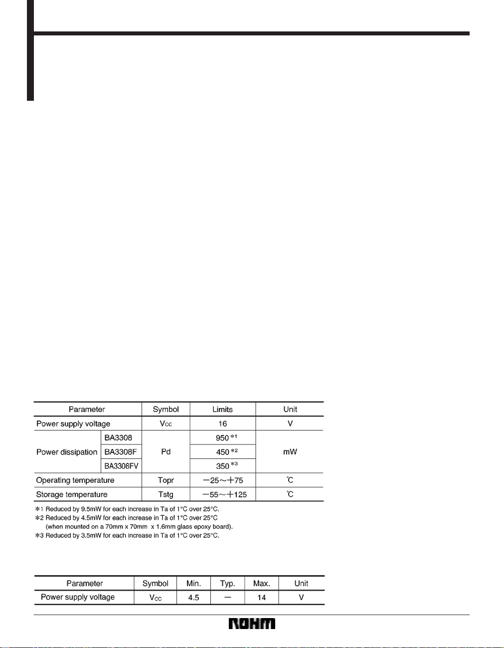
use in stereo radio-cassette recorders and tape recorders. They come in compact 9-pin SIP (BA3308), 14-pin MF
(BA3308F) and 14-pin SSOP (BS3308FV) packages, and have two record/playback preamplifiers, and an ALC circuit.
The preamplifiers have high gain and low distortion, and can be directly coupled to the tape head without coupling capacitors. This prevents tape head magnetization and “pop” noise generation.
A built-in rectifier means that an ALC circuit with good channel balance and large dynamic range can be constructed
with addition of just an external time constant circuit.
The ICs also include power-on mute circuits that suppress “pop” noise generation.
Applications
Stereo radio cassette recorders, cassette decks and
home stereo systems and music centers
Features
1) Built-in ALC rectifier diode.
2) Wide operating power supply voltage range (V
4.5V to 14V).
3) Low current dissipation (I
4) High gain (G
5) Low distortion (THD = 0.1%).
VO = 80dB).
Q = 3.5mV).
CC =
6) Low noise (V
7) Input coupling capacitors and not necessary.
8) Good ALC channel balance.
9) Power-on mute circuit.
10) ALC dynamic range can be varied by the addition
of an external input resistor.
NIN = 1µVrms)
Absolute maximum ratings (Ta = 25C)
Recommended operating conditions (Ta = 25C)
193
Audio ICs BA3308 / BA3308F / BA3308FV
Block diagram
Electrical characteristics (unless otherwise noted, Ta = 25C, V
194
CC = 7.0V, f = 1kHz and BPF: 20Hz to 20kHz)
Audio ICs BA3308 / BA3308F / BA3308FV
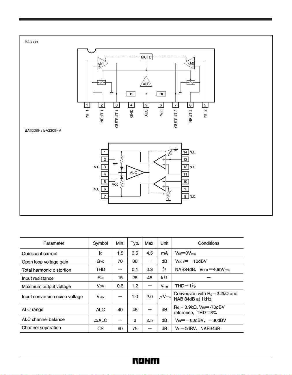
Measurement circuit
Application example Application example circuit PCB (copper side)
195

Audio ICs BA3308 / BA3308F / BA3308FV
Total application circuit
Circuit operation
(1) Recording
(1) Recording amplifier (See Fig. 5)
The channel 1 and 2 amplifier input stages of the BA3308
(pins 8 and 2) can be direct-coupled, and the input coupling capacitors C
1 and C2 are not particularly required.
The voltage gain of the recording amplifier is given by G
= R5/R3, but as a “pop” noise is generated when power
is applied, (see “operation notes”), use the time constant
circuit values given for C
3 and R3 (C4 and R4) in the ap-
plication example circuit diagram, or values close to
these, and adjust the voltage gain with R
5 (R6). R5 (R6) is
also the DC bias feedback resistor, and is connected between pin 3 (7), and the output capacitor C
5 (C6).
(2) ALC (See Fig. 6)
The BA3308 includes a signal rectifier block and electronic potentiometers required for the ALC. In the signal
rectifier block, a comparator compares the DC output
voltage component of the output stage signal (pins 3 and
7) to a voltage of 4.5V
F (1VF is about 0.7V, so 4.5VF is
approximately 3V), and if it is above this, the comparator
switches on, and charges the smoothing capacitor C
The operating point of the amplifier’s ch1 and ch2 output
stages is fixed at 3V
F (an effective value of approximately 0.75V), the
is 1.5V
F, so when the signal output voltage
comparator goes on, DC signals for electronic potentiometer control are generated, and the ALC starts operating.
The electronic potentiometers are connected between
V
the input lines (pins 2 and 8) and GND, and the input signals is attenuated by the ratio of the electronic potentiometer resistances and the external resistors R
range of the ALC can be varied by the values of R
2, but if they are too large the S/N ratio will worsen. Suf-
R
ficient ALC range should be obtained with R
ues of around several kohms. C
7 and R7 connected to pin
5 set the ALC attack and recovery times. The larger the
values of these constants, the longer the recovery time,
and the smaller the value of C
7 the shorter the attack
time.
7.
1 and R2. The
1 and
1 and R2 val-
196

Audio ICs BA3308 / BA3308F / BA3308FV
(2) Playback (See Fig. 7)
During playback, the ch1 and ch2 amplifiers are used as
NAB equalizer amplifiers, and time constant circuits are
connected between pins 1 and 3, and 7 and 9 in the negative-feedback section to give the NAB characteristics.
The voltage gain is given by:
G
V = R11 R9 / (I jϖC9 R9) /R3
In the same way as for recording, the NAB time constant
circuit is adjusted to give the required gain (to prevent
generation of a “pop” noise when power is applied). The
output stage (pins 3 and 7) operating point is fixed at 3V
Therefore, as indicated in the V
(see Fig. 19), even if the V
Max. vs, VCC characteristic
CC voltage is made larger than
5V, the maximum output voltage will not exceed 1.2V
(typ.). The ALC circuit is not required for playback, so pin
5 is grounded. The S/N ratio during playback is better if
the external resistors R
1 and R2 that are connected to the
input pins (2 and 8) for recording are switched out.
F.
197

Audio ICs BA3308 / BA3308F / BA3308FV
Operation notes
The BA3308 has a built-in power-on mute circuit to prevent generation of a “pop” sound when the power is applied. The generation of the “pop” sound is prevented by
the DC blocking capacitors C
3 and C4 connected to pins
1 and 9, and the charge time required for the ripple filter
capacitor C
T o ensure correct operation of this circuit, use the values
given in the application example circuit for C
8 and R8.
C
8 that is connected to pin 6.
3, C4, R3, R4,
Application board component layout (component side)
198

Audio ICs BA3308 / BA3308F / BA3308FV
Electrical characteristics curves
199

Audio ICs BA3308 / BA3308F / BA3308FV
External dimensions (Units: mm)
200
 Loading...