

t
Datashee
2A/1A Fixed Output LDO Regulators
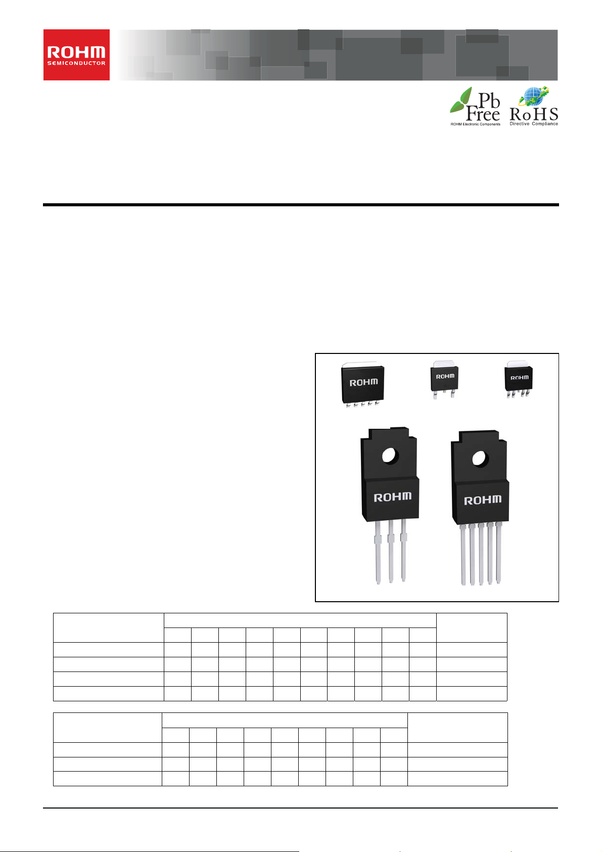
BAxxDD0T Series BAxxCC0T Series BAxxCC0FP Series
2A/1A Fixed Output LDO Regulators
With Shutdown Swicth
BAxxDD0WT Series BAxxDD0HFP Series BAxxCC0WT Series BAxxCC0WFP Series
●General Description
Standard Fixed Output LDO Regulators are low-saturation regulators, available for output s up to 2A / 1A. ROHM has a
wide output voltage range and package lineup with and without shutdown switches. This IC has a built-in over-current
protection circuit that prevents the destruction of the IC due to output short circuits, a thermal shut-down circuit that protects
the IC from damage due to overloading and an over-voltage protection circuit that protects the IC from surges generated in
the power supply line of the IC.
●Features
±1% highly accurate output voltage (BAxxDD0xx)
Low saturation with PNP output
Built-in over-current protection circuit that prevents
the destruction of the IC due to output short circuits
Built-in thermal shutdown circuit for protecting the IC
from damage due to overloading
Built-in over- voltage protection circuit that prevents
the destruction of the IC due to power supply surges
●Key Specification
Input Power Supply Voltage: 25V (Max.)
Output voltage type: Fixed
Output current: BAxxDD0xx series 2A (Max.)
BAxxCC0xx series 1A (Max.)
Shutdown current: 0μA(Typ.)
Operating temperature range: -40℃ to +125℃
●Applications
Used in DSP power supplies for DVD and CD players,
FPDs, televisions, personal computers or any other
consumer device
●Lineup matrix
■1A output BAxxCC0xx Series
Part Number
BAxxCC0WT
BAxxCC0WFP - ○ ○ ○ ○ ○ ○ - ○ - TO252-5
BAxxCC0T ○ ○ ○ ○ ○ ○ ○ ○ ○ ○ TO220FP-3
BAxxCC0FP ○ ○ ○ ○ ○ ○ ○ ○ ○ ○ TO252-3
■2A output BAxxDD0xx Series
Part Number
BAxxDD0WT ○ ○ ○ ○ ○ ○ ○ ○ ○ TO220FP-5
BAxxDD0WHFP ○ ○ ○ ○ ○ ○ ○ ○ ○ HRP5
BAxxDD0T
3.0 3.3 5.0 6.0 7.0 8.0 9.0 10.0 12.0 15.0
○ ○ ○ - ○ ○ ○ ○ ○ -
1.5 1.8 2.5 3.0 3.3 5.0 9.0 12.0 16.0
○ ○ ○ ○ ○ ○ ○ ○ ○
Output voltage (V)
Output voltage (V)
●Packages W (Typ.) x D (Typ.) x H (Max.)
HRP5 9.395mm x 10.54mm x 2.005mm
TO252-3 6.50 mm x 9.50mm x 2.50 mm
TO252-5 6.50 mm x 9.50mm x 2.50 mm
TO220FP-3 10.00 mm x 30.50mm x 4.60 mm
TO220FP-5 10.00 mm x 30.50mm x 4.60 mm
HRP5
TO252-3
TO220FP-5
Package
TO220FP-3
TO252-5
TO220FP-5 TO220FP-3
Package
○Product structure : Silicon monolithic integrated circuit ○This product is not designed protection against radioactive rays.
www.rohm.com
© 2012 ROHM Co., Ltd. All rights reserved.
TSZ22111・14・001
1/20
TSZ02201-0R6R0A600130-1-2
26.Jun.2012 Rev.001
BAxxDD0xx BAxxCC0xx
●Ordering Information
Datasheet
B A x x x x 0 x x x x
Part
Number
Output voltage
Output
Current
CC0 : 1A
DD0 : 2A
Shutdown Switch
W : Includes switch
None: without switch
Package
HFP
FP
T
: HRP5
: TO252-5
: TO252-3
: TO220FP-5
: TO220FP-3
- x x
Packaging and forming specification
TR: Embossed tape and reel
(HRP5)
E2: Embossed tape and reel
(TO252-3,TO252-5)
None : Container Tube
(TO220FP-3,TO220FP-5)
●Lineup
■1A output BAxxCC0xx Series
Maximum output
current (Max.)
Shutdown
Switch
Package
Output
voltage(Typ.)
Orderable
Part Number
3.3V BA033CC0WFP-E2
5.0V BA05CC0WFP-E2
6.0V BA06CC0WFP-E2
TO252-5 Reel of 2000
7.0V BA07CC0WFP-E2
8.0V BA08CC0WFP-E2
9.0V BA09CC0WFP-E2
12.0V BAJ2CC0WFP-E2
With Switch
3.0V BA03CC0WT
3.3V BA033CC0WT
5.0V BA05CC0WT
TO220FP-5 Tube of 500
7.0V BA07CC0WT
8.0V BA08CC0WT
9.0V BA09CC0WT
10.0V BAJ0CC0WT
12.0V BAJ2CC0WT
3.0V BA03CC0FP-E2
3.3V BA033CC0FP-E2
1A
5.0V BA05CC0FP-E2
6.0V BA06CC0FP-E2
TO252-3 Reel of 2000
7.0V BA07CC0FP-E2
8.0V BA08CC0FP-E2
9.0V BA09CC0FP-E2
10.0V BAJ0CC0FP-E2
12.0V BAJ2CC0FP-E2
No switch
15.0V BAJ5CC0FP-E2
3.0V BA03CC0T
3.3V BA033CC0T
5.0V BA05CC0T
6.0V BA06CC0T
TO220FP-3 Tube of 500
7.0V BA07CC0T
8.0V BA08CC0T
9.0V BA09CC0T
10.0V BAJ0CC0T
12.0V BAJ2CC0T
15.0V BAJ5CC0T
www.rohm.com
© 2012 ROHM Co., Ltd. All rights reserved.
TSZ22111・15・001
2/20
TSZ02201-0R6R0A600130-1-2
26.Jun.2012 Rev.001

BAxxDD0xx BAxxCC0xx
■2A output BAxxDD0xx Series
Maximum output
current (Max.)
2A
Shutdown
Switch
With Switch
No switch TO220FP-3 Tube of 500
Package
TO220FP-5 Tube of 500
HRP5 Reel of 2000
Output
voltage(Typ.)
1.5V BA15DD0WT
1.8V BA18DD0WT
2.5V BA25DD0WT
3.0V BA30DD0WT
3.3V BA33DD0WT
5.0V BA50DD0WT
9.0V BA90DD0WT
12.0V BAJ2DD0WT
16.0V BAJ6DD0WT
1.5V BA15DD0WHFP-TR
1.8V BA18DD0WHFP-TR
2.5V BA25DD0WHFP-TR
3.0V BA30DD0WHFP-TR
3.3V BA33DD0WHFP-TR
5.0V BA50DD0WHFP-TR
9.0V BA90DD0WHFP-TR
12.0V BAJ2DD0WHFP-TR
16.0V BAJ6DD0WHFP-TR
1.5V BA15DD0T
1.8V BA18DD0T
2.5V BA25DD0T
3.0V BA30DD0T
3.3V BA33DD0T
5.0V BA50DD0T
9.0V BA90DD0T
12.0V BAJ2DD0T
16.0V BAJ6DD0T
Orderable
Part Number
Datasheet
www.rohm.com
© 2012 ROHM Co., Ltd. All rights reserved.
TSZ22111・15・001
3/20
TSZ02201-0R6R0A600130-1-2
26.Jun.2012 Rev.001
BAxxDD0xx BAxxCC0xx
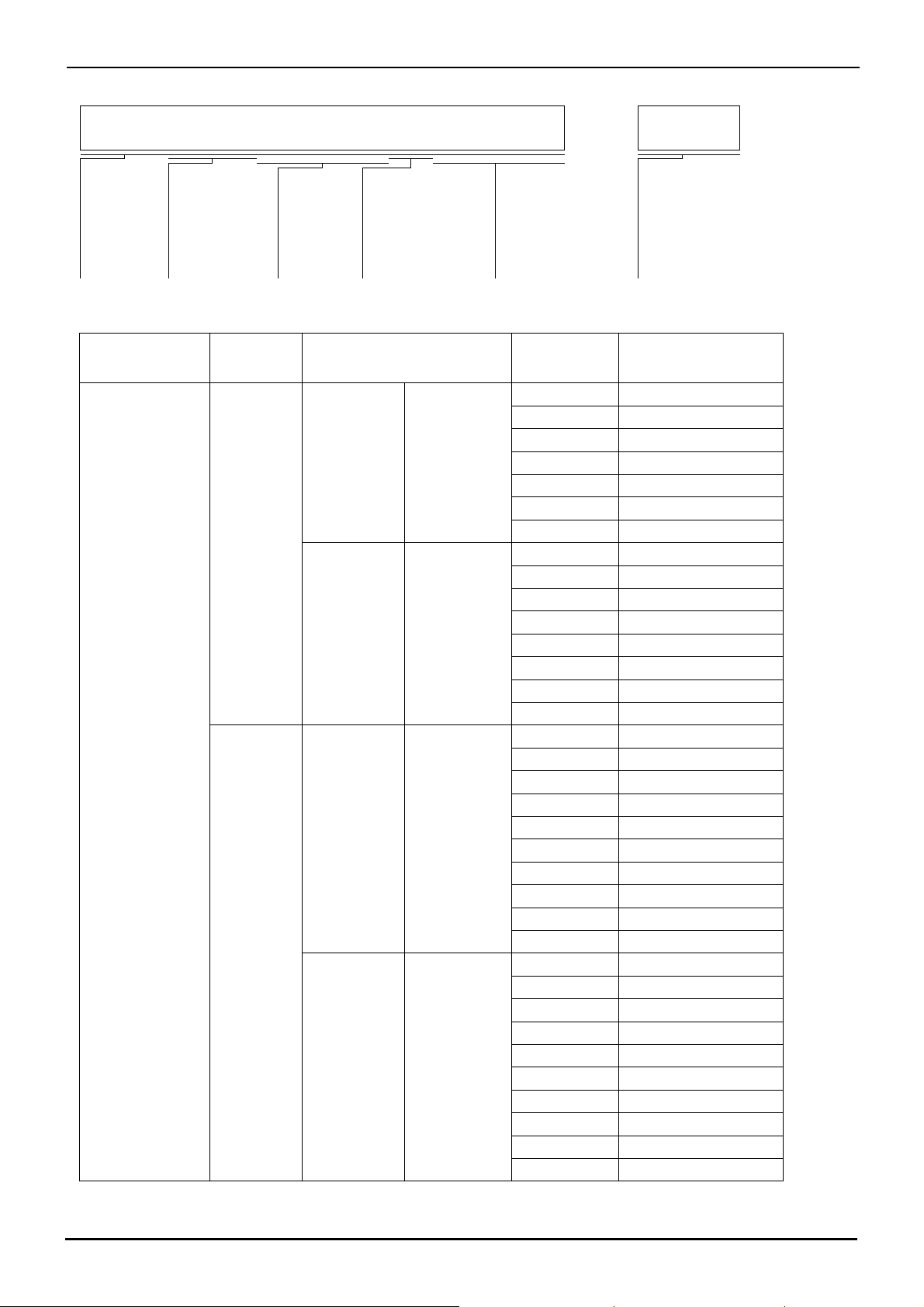
●Block Diagrams / Pin Configurations / Pin Descriptions
BAxxCC0WFP/ BAxxDD0WHFP/ BAxxCC0WT/ BAxxDD0WT
GND(TO252-5・HRP5)
Fin
Datasheet
Vcc
Vref
OVP TSD OCP
1 2
CTL Vcc N.C.
Driver
4
3
OUT N.C.
(TO252-5)
GND
(TO220FP-5,HRP5)
Fig.1
R2
R1
5
TOP VIEW
FIN
PIN No. Pin Name Function
1 CTL Output voltage ON/OFF control
2 Vcc Power supply voltage input
3 N.C./GND Unconnected terminal/GND*1
4 OUT Voltage output
5 N.C. Unconnected terminal
Fin GND GND*2
1
*
TO252-5=N.C.,TO220FP-5,HRP5=GND
2
*
TO252-5,HRP5 only
1 2 3 4 5
TO220FP-5
1 2 3 4 5
TO252-5
1 2 3 4 5
HRP5
BAxxCC0T/ BAxxCC0FP/ BAxxDD0T
TOP VIEW
1
TO252-3
FIN
2
3
1
2 3
TO220FP-3
Vref
Vcc
1
OVP TSD OCP
Fin
2
N.C.
(TO252-3)
GND
(TO220FP-3)
Fig.2
GND(TO252-3)
Vcc
Driver
R2
R1
3
OUT
PIN No. Pin Name Function
1 Vcc Power supply voltage input
2 N.C./GND Unconnected terminal/GND*1
3 OUT Voltage output
Fi GND GND*2
1
*
TO252-3=N.C.,TO220FP-3=GND
2
*
TO252-3 only
www.rohm.com
© 2012 ROHM Co., Ltd. All rights reserved.
TSZ22111・15・001
4/20
TSZ02201-0R6R0A600130-1-2
26.Jun.2012 Rev.001
BAxxDD0xx BAxxCC0xx
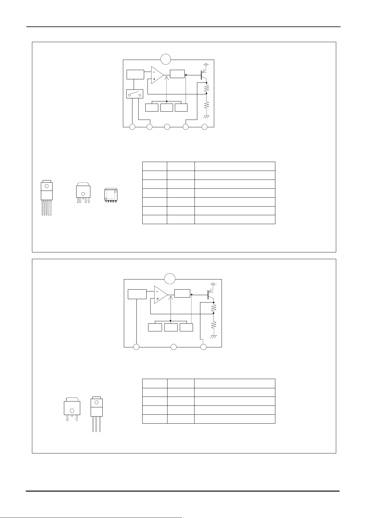
●Absolute Maximum Ratings (Ta=25℃)
Parameter Symbol Ratings Unit
Datasheet
Input Power Supply Voltage*1 V
-0.3 to +35 V
CC
2300(HRP5)
Power Dissipation*2 Pd
1300(TO252-5)
1200(TO252-3)
2000(TO220FP-3,5)
Operating Temperature Range Topr -40 to +125 ℃
Ambient Storage Temperature Tstg -55 to +150 ℃
Junction Temperature Tj
+150 ℃
MAX.
Output Control Terminal Voltage*3 Vctl -0.3 to +Vcc V
Voltage Applied to the Tip *4 VCC peak +50 V
*1 Must not exceed Pd
*2 HRP5 : In cases in which Ta≧25℃ when a 70mm×70mm×1.6mm glass
epoxy board is used, the power is reduced by 18.4 mW/℃.
TO252FP-3 : In cases in which Ta≧25℃ when a 70mm×70mm×1.6mm glass
epoxy board is used, the power is reduced by 9.6 mW/℃.
TO252FP-5 : In cases in which Ta≧25℃ when a 70mm×70mm×1.6mm glass
epoxy board is used, the power is reduced by 10.4 mW/℃.
TO220FP-5 : No heat sink. When Ta≧25℃, the power is reduced by 16 mW/℃.
*3 Only for models with shutdown switches.
*4 Applied voltage : 200msec or less (tr≥1msec)
50V
35V
0V
●Recommended Operating Ratings (Ta=25℃)
Parameter Symbol
Input
Power Supply
Voltage
Output Current
BAxxCC0xx
BAxxDD0xx 3.0 ― 25.0 V
BAxxCC0xx
BAxxDD0xx ―
V
CC
Io
Min. Typ. Max.
4.0
―
Output Control Terminal Voltage Vctl 0 ― V
Ratings
―
―
―
25.0 V
1 A
2 A
V
CC
mW
tr≧1msec
MAX200msec
(Voltage Supply more than 35V)
Unit
www.rohm.com
© 2012 ROHM Co., Ltd. All rights reserved.
TSZ22111・15・001
5/20
TSZ02201-0R6R0A600130-1-2
26.Jun.2012 Rev.001

BAxxDD0xx BAxxCC0xx
*7
Datasheet
●Electrical Characteristics
BAxxCC0 Series (Unless otherwise specified, Ta=25℃, V
Parameter Symbol
Output Voltage *6 Vo
Min. Typ. Max.
Vo(T)×
0.98
CTL=5V, Io=500mA Setting
Limit
Vo(T)
Vo(T)×
1.02
Unit Conditions
V
*5)
Shut Down Current Isd - 0 10 μA VCTL=0V
Bias Current Ib
-
2.5 5.0 mA VCTL=2V, Io=0mA
Dropout Voltage ΔVd - 0.3 0.5 V Vcc=Vo×0.95
Peak Output Current Io 1.0
Ripple Rejection R.R. 45 55 - dB
Line Regulation Reg.I
-
- -
A
f=120Hz,
Io=100mA
20 100 mV
Vcc=Vo(T)+1→25V
ein
=1Vrms,
Load Regulation Reg.L - 50 150 mV Io=5mA→1A
Temperature Coefficient of
Output Voltage
*8
Tcvo
- ±0.02 - %/℃ Io=5mA,Tj=0 to 125℃
Output Short Current Ios - 0.40 - A Vcc=25V
ON Mode Voltage VthH 2.0
- -
V ACTIVE MODE, Io=0mA
OFF Mode Voltage VthL - - 0.8 V OFF MODE, Io=0mA
Input High Current ICTL 100 200 300 μA VCTL=5V, Io=0mA
BAxxDD0 series (Unless otherwise specified, Ta=25℃, VCTL=3V, Vcc=VCCT*9)
Parameter Symbol
Shut Down Current Isd
Bias Current Ib - 0.9 2.0 mA Io=0mA
Output Voltage
Dropout Voltage 1
Dropout Voltage 2
Peak Output Current Io 2.0
Ripple Rejection R.R. - 55 - dB f=120Hz, ein*7=-20dBV, Io=100mA
Line Regulation Reg.I
Load Regulation Reg.L - 50 200 mV Io=0mA→2A
Temperature Coefficient of
Output Voltage
CTL ON Mode Voltage Von 2.0 - Vcc V ACTIVE MODE, Io=0mA
CTL OFF Mode Voltage Voff - - 0.8 V OFF MODE, Io=0mA
CTL Input Current ICTL - 60 120 μA VCTL=3V, Io=0mA
*5 Vo=3.3V:Vcc=8.3V, Vo=5V:Vcc=10V, Vo=6V:Vcc=11V, Vo=7V:Vcc=12V, Vo=8V:Vcc=13V, Vo=9V:Vcc=14V, Vo=12V:Vcc=17V
*6 Vo(T)=3.3, 5. 0 , 6.0, 7. 0, 8.0, 9.0,12V
*7 ein : Input Voltage Ripple
*8 Not 100% tested
*9 Vo=1.5V,1.8V,2.5V,3.0V:VCCT =4.0V、Vo=3.3V,5.0V:VCCT =7.0V、Vo=9V:VCCT =12.0V、Vo=12V:VCCT =14.0V、Vo=16V:VCCT =18.0V)
*10 Votyp=1.5V,1.8V,2.5V,3.0V,3.3V,5.0V,9.0V,12.0V,16.0V
*
11 Vo≧3.0V
*10
Vo
*11
*11
ΔVd2 - 0.45 0.7 V Vcc=0.95×Vo, Io=2A
*8
ΔVd1 -
Tcvo - ±0.02 - %/℃ Io=5mA, Tj=0 to 125℃
Min. Typ. Max.
-
Votyp×
0.99
-
Limit
0 10 μA VCTL=0V, Io=0mA
Votyp
Votyp×
1.01
0.3 0.5 V
- -
15 50 mV
Unit Conditions
V Io=200mA
Vcc=0.95×Vo, Io=1A
A
Vcc=VCCT*9V→25V, Io=200mA
www.rohm.com
© 2012 ROHM Co., Ltd. All rights reserved.
TSZ22111・15・001
6/20
TSZ02201-0R6R0A600130-1-2
26.Jun.2012 Rev.001
BAxxDD0xx BAxxCC0xx
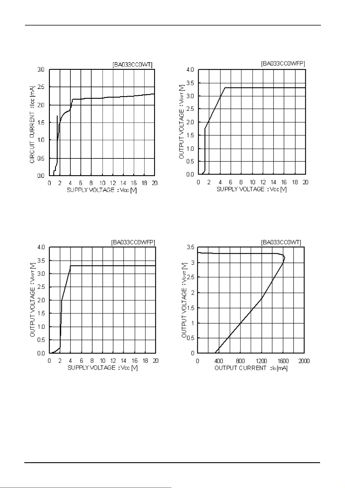
●Typical Performance Curves
(Unless specified otherwise, Vcc=8.3V, Vo=3.3V, V
BAxxCC0xx (BA33CC0WT)
=5.0V, and Io=0mA)
CTL
Datasheet
Fig.3
Circuit current
Fig.4
Input Stability
Fig.5
Input Stability
(Io=500mA)
www.rohm.com
© 2012 ROHM Co., Ltd. All rights reserved.
TSZ22111・15・001
7/20
Fig.6
Load Stability
TSZ02201-0R6R0A600130-1-2
26.Jun.2012 Rev.001

BAxxDD0xx BAxxCC0xx
●Typical Performance Curves - continued
Datasheet
Fig.7
Input/Output Voltage Difference
Io-△Vd Characteristics (Vcc=2.95V)
Fig.8
Ripple Rejection Characteristics
(Io=100mA)
Fig.9
Output Voltage
Temperature Characteristics
www.rohm.com
© 2012 ROHM Co., Ltd. All rights reserved.
TSZ22111・15・001
8/20
Fig.10
Circuit Current by load Level
(IOUT=0mA→1A)
TSZ02201-0R6R0A600130-1-2
26.Jun.2012 Rev.001

BAxxDD0xx BAxxCC0xx
●Typical Performance Curves - continued
Datasheet
Fig.11
CTL Voltage vs. CTL Current
Fig.12
CTL Voltage vs. Output Voltage
Fig.13
Overvoltage Operating
Characteristics (Io=200mA)
www.rohm.com
© 2012 ROHM Co., Ltd. All rights reserved.
TSZ22111・15・001
9/20
Fig.14
Thermal Shutdown
Circuit Characteristics
TSZ02201-0R6R0A600130-1-2
26.Jun.2012 Rev.001

BAxxDD0xx BAxxCC0xx
●Typical Performance Curves - continued
(Unless specified otherwise, Vcc=7.0V, Vo=5.0V, V
BAxxDD0xx (BA50DD0WT)
Datasheet
CTL=3.0V, and Io=0mA)
Fig.15
Circuit Current
Fig.16
Input Stability (Io=0mA)
Fig.17
Input Stability (Io=2A)
www.rohm.com
© 2012 ROHM Co., Ltd. All rights reserved.
TSZ22111・15・001
10/20
Fig.18
Load Stability
TSZ02201-0R6R0A600130-1-2
26.Jun.2012 Rev.001

BAxxDD0xx BAxxCC0xx
●Typical Performance Curves - continued
Datasheet
Fig.19
Input/Output Voltage Difference
Fig.20
Ripple Rejection Characteristics
Fig.21
Temperature Characteristics
www.rohm.com
© 2012 ROHM Co., Ltd. All rights reserved.
TSZ22111・15・001
11/20
Fig.22
Circuit Current by Load Level
(lout=0mA→2A)
TSZ02201-0R6R0A600130-1-2
26.Jun.2012 Rev.001

BAxxDD0xx BAxxCC0xx
●Typical Performance Curves - continued
Datasheet
[BA50DD0WT]
[V]
Fig.23
CTL Voltage vs. CTL Current
Fig.24
CTL Voltage vs. Output Voltage
Fig.25
Overvoltage Operating
(lo=200mA)
www.rohm.com
© 2012 ROHM Co., Ltd. All rights reserved.
TSZ22111・15・001
12/20
Fig.26
Thermal Shutdown
Circuit Characteristics
TSZ02201-0R6R0A600130-1-2
26.Jun.2012 Rev.001

BAxxDD0xx BAxxCC0xx
)
3
●I/O equivalence circuit
<BAxxDD0xx Series> <BAxxCC0xx Series>
OUT
25kΩ
CTL
25kΩ
CTL
Vcc
39kΩ 2kΩ
31kΩ
10kΩ
Vcc
Vcc
R2
R1
Fig.27
●Power Dissipation
HRP-5
10
Board size : 70×70×1.6 ㎜
Board front copper foil area : 10.5×10.5 ㎜
9
①2-layer board (back surface copper foil area :15×15 ㎜
②2-layer board (back surface copper foil area :70×70 ㎜2)
8
③4-layer board (back surface copper foil area :70×70 ㎜
7
③7.3W
6
5
②5.5W
4
3
Power Dissipation:Pd(W)
2
①2.3W
1
0
0 25 50 75 100 125 150
Ambient temperature:Ta(
(board contains a thermal via)
Fig.29
℃)
2
2
)
2
)
TO220FP-5
25
When using a maximum heat sick :
When using an IC alone :
20
(1)20.0
15
10
Power Dissipation:Pd(W
5
(2)2.0
0
0 25 50 75 100 125 150
Ambient temperature:Ta(℃)
Fig.30
10kΩ
Fig.28
θj-c=6.25(℃/W)
θj-6=62.5(℃/W)
Datasheet
Vcc
R2
R1
OUT
TO252-5
2.0
Mounted on a Rohm standard board
Board size : 70
Copper foil area :7
1.6
TO252-5
1.30
1.2
0.8
Power Dissipation:Pd(W)
0.4
0.0
0 25 50 75 100 125 150
×70×1.6 ㎜
×7 ㎜
θja=96.2(℃/W)
Ambient temperature:Ta(
℃)
Fig.31
www.rohm.com
© 2012 ROHM Co., Ltd. All rights reserved.
TSZ22111・15・001
13/20
TSZ02201-0R6R0A600130-1-2
26.Jun.2012 Rev.001

BAxxDD0xx BAxxCC0xx
Datasheet
When using at temperatures over Ta=25℃, please refer to the heat reducing characteristics shown in Fig.29 through 31.
The IC characteristics are closely related to the temperature at which the IC is used and if the temperature exceeds the
maximum junction temperature Tj
MAX., the elements may be damaged or destroyed. From the standpoints of instantaneous
destruction and long-term operating reliability, it is necessary give sufficient consideration to IC heat. In order to protect the
IC from thermal damage, it is necessary to operate it at temperatures lower than the maximum junction temperature TjMAX
of the IC.
Fig.30 shows the acceptable loss and heat reducing characteristics of the TO220FP package The portion shown by the
diagonal line is the acceptable loss range that can be used with the IC alone. Even when the ambient temperature Ta is a
normal temperature (25℃), the chip (junction) temperature Tj may be quite high so please operate the IC at temperatures
less than the acceptable loss Pd.
The method of calculating the power consumption Pc (W) is as follows.
Pc = (Vcc-Vo) × Io + Vcc × Icca
Acceptable loss Pd≦Pc
Vcc:
Input voltage
Vo:
Output voltage
Io:
Load current
Vcca:
Circuit current
Solving this for load current I
Io≦
(Please refer to Fig.10 and 22 for Icca.)
Pd – Vcc×Icca
Vcc-Vo
It is then possible to fin d the maxi mu m load cu r rent Io
in order to operate within the acceptable loss:
O
MAX with respect to the applied volt age Vcc at the ti me of therma l design .
・Calculation Example
Example 1) When Ta=85℃, Vcc=8.3V, Vo=3.3V, BA33DD0WT
1.04-8.3×Icca
Io≦ With the IC alone : θja=62.5℃/W → -16mW/℃
5
Io≦200mA (Icca : 2mA) 25℃=2000mW → 85℃=1040mW
Please refer to the above information and keep thermal designs within the scope of acceptable loss for all oper ating
temperature ranges.
The power consumption Pc of the IC when there is a short circuit (short between Vo and GND) is:
Pc=Vcc×(Icca+Ishort)
*Ishort: Short circuit current
●Peripheral Circuit Considerations
・Vcc Terminal
Please attach a capacitor (greater than 0.33µF) between the Vcc and GND.
The capacitance values will differ depending on the application, so please t ake this in to acco unt w hen configuring the termin al.
・GND Terminal
Please be sure to keep the set ground and IC ground at the same potential lev el so that a potential difference does not
arise between them.
If a potential difference arises between the set ground and the IC ground, the preset voltage will not be outputted,
causing the system to become unstable. Therefore, please reduce the impedance b y making the grou nd patterns as wide
as possible and by reducing the distance between the set ground and the IC ground as much as possible.
・CTL Terminal
The CTL terminal is turned ON at 2.0V and higher and OFF at 0.8V and low er wi thin the operating pow er supply volt age range.
The power supply and the CTL terminal may be started up and shut down in any order without problems.
0.1
EFFECTIVE SERIES RESISTANCE:ESR [Ω]
100
Unstable operating region
10
Stable operating region
1
1
10
Unstable operating region
100
OUTPUT CURRENT:lo(mA)
1000
●Vo Terminal
IC
100
22μF
10
1
EFFECTIVE SERIES RESISTANCE:ESR [Ω]
0.1
0
Unstable operating region
Stable operating region
Unstable operating region
400
600
200
OUTPUT CURRENT:lo(mA)
800
1000
OUT
Fig.32 Output Equivalent Circuit Fig.33 ESR-Io Characteristics Fig.34 ESR vs. Io Characteristics
(BAxxCC0) (BAxxDD0)
Please attach an anti-oscillation capacitor between V
o and GND. The capacitance of the capacitor may significantly change
due to factors such as temperature changes, making it impossible to completely stop oscillations. Please use a tantalum
capacitor or aluminum electrolysis capacitor with favorable characteristics and small internal series resistance (ESR) even
at low temperatures. The output fluctuates regardless of whether the ESR is large or small. Please use the IC within the
stable operating region while referring to the ESR characteristics reference data shown in Fig.32 through 34. In applications
where there are sudden load fluctuations, the use of a capacitor with large capacitance is recommended.
10000
www.rohm.com
© 2012 ROHM Co., Ltd. All rights reserved.
TSZ22111・15・001
14/20
TSZ02201-0R6R0A600130-1-2
26.Jun.2012 Rev.001

BAxxDD0xx BAxxCC0xx
Datasheet
●Operational Notes
1) Protection Circuits
Over-current Protection Circuit
A built-in over-current protection circuit correspond ing to the current capacity pr events the destruction of the IC when there
are load shorts. This protection circuit is a “7”-shap ed curren t control circuit that is designed such that the current is restricted
and does not latch even when a large current momentarily flows through the system with a high-capacitance capacitor.
However, while this protection circuit is e ffective f or the prevention of destruction due to unexpected accidents, it is not
suitable for continuous operation or transient use. Please be aware when creating thermal designs that the overcurrent
protection circuit has negative current capacity characteristics with regard to temperature (Refer to Fig.6 and 18).
Thermal Shutdown Circuit (Thermal Protection)
This system has a built-in temperature protection circuit for the purpose of protecting the IC from thermal damage.
As shown above, this must be used within the range of acceptable loss, but if the acceptable loss happens to be
continuously exceeded, the chip temperature Tj increases, causing the temperature protection circuit to operate.
When the thermal shutdown circuit operates, the operation of the circuit is suspended. The circuit resumes op eration
immediately after the chip temperature Tj decreases, so the output repeats the ON and OFF states (Please refer to
Fig.14 and 26 for the temperatures at which the temperature protection circuit operates).
There are cases in which the IC is destroyed due to thermal runaway when it is left in the ov erloaded state. Be sure to
avoid leaving the IC in the overloaded state.
Reverse Current
In order to prevent the destruction of the IC when a reverse current flows through the IC, it is recommended that a diode
be placed between the Vcc and Vo and a pathway be created so that the current can escape (Refer to Fig.35).
Reverse current
Vcc
CTL
OUT
GND
Fig.35 Bypass diode
2) This IC is bipolar IC that has a P-board (substrate) and P+ isolation la yer between each devise, as shown in Fig.36. A
P-N junction is formed between this P-layer and the N-layer of each device, and the P-N junction operates as a parasitic
diode when the electric potential relationship is GND> Pin A, GND> Pin B, while it operates as a parasitic transistor when
the electric potential relationship is Pin B GND> Pin A. Parasitic devices are structurally inevitable in the IC. The
operation of parasitic devices induces mutual interference between circuits, causing malfunctions and eventually the
destruction of the IC. It is necessary to be careful not to use the IC in ways that would cause parasitic elements to
operate. For example, applying a voltage that is lower than the GND (P-board) to the input terminal.
(Pin A)
Resistor
P+
N
P
N
P+
P
Parasitic element
GND
N
Fig.36 Example of the basic structure of a bipolar IC
Transistor (NPN)
(Pin B)
C
P+
N
Parasitic element
or transistor
B
E
P
N
N
P
GND
GND
P+
N
(Pin B)
(Pin A)
C
B
E
GND
GND
Parasitic element
or transistor
Parasitic element
Status of this document
The Japanese version of this document is formal specification. A customer may use this translation version only for a reference
to help reading the formal version.
If there are any differences in translation version of this doc
www.rohm.com
© 2012 ROHM Co., Ltd. All rights reserved.
TSZ22111・15・001
ument formal version takes priority.
15/20
TSZ02201-0R6R0A600130-1-2
26.Jun.2012 Rev.001

BAxxDD0xx BAxxCC0xx
●Physical Dimension Tape and Reel Information
HRP5
9.395±0.125
(MAX 9.745 include BURR)
8.82 ± 0.1
(6.5)
1.905±0.1
<Tape and Reel information>
8.0±0.13 1.017±0.2
1.2575
1.72
0.08±0.05
54321
0.73±0.1
0.08 S
(7.49)
S
0.835±0.2
1.523±0.15
+5.5°
4.5°
−4.5°
+0.1
0.27
−0.05
(Unit : mm)
10.54±0.13
TO252-3
6.5±0.2
+0.2
5.1
-
FIN
C0.5
0.1
2.3±0.2
0.5±0.1
<Tape and Reel information>
5.5±0.2 1.5±0.2
0.65
0.75
2.3±0.2
21 3
0.8
0.65
2.3±0.2
0.5±0.1
1.0±0.2
9.5±0.5
1.5
2.5
(Unit : mm)
TO252-5
6.5±0.2
+0.2
5.1
-
0.1
C0.5
2.3±0.2
0.5±0.1
<Tape and Reel information>
5.5±0.2 1.5±0.2
123 54
0.5
FIN
9.5±0.5
1.5
0.8
1.27
2.5
0.5±0.1
1.0±0.2
TO220FP-3
+0.4
−0.2
17.0
+0.3
10.0
−0.1
+0.3
7.0
−0.1
φ
1.8±0.2
12.0±0.2
8.0±0.2
3.2±0.1
+0.3
4.5
−0.1
(Unit : mm)
+0.2
2.8
−0.1
Embossed carrier tapeTape
Quantity
Direction
of feed
2000pcs
TR
The direction is the 1pin of product is at the upper right when you hold
( )
reel on the left hand and you pull out the tape on the right hand
Reel
Embossed carrier tapeTape
Quantity
Direction
of feed
2000pcs
E2
The direction is the 1pin of product is at the lower left when you hold
( )
reel on the left hand and you pull out the tape on the right hand
Reel
Embossed carrier tapeTape
Quantity
Direction
of feed
2000pcs
E2
The direction is the 1pin of product is at the lower left when you hold
( )
reel on the left hand and you pull out the tape on the right hand
Reel
<Tape and Reel information>
TubeContainer
Quantity
Direction of feed
500pcs
Direction of products is fixed in a container tube
1pin
Direction of feed
Order quantity needs to be multiple of the minimum quantity.
∗
1pin
Order quantity needs to be multiple of the minimum quantity.
∗
1pin
Order quantity needs to be multiple of the minimum quantity.
∗
Direction of feed
Direction of feed
Datasheet
231
1.3
0.8
2.54±0.5
0.55
+0.1
−0.05
13.5Min.
5.0±0.2
2.54±0.5
www.rohm.com
© 2012 ROHM Co., Ltd. All rights reserved.
TSZ22111・15・001
2.6±0.5
(Unit : mm)
16/20
Order quantity needs to be multiple of the minimum quantity.
∗
TSZ02201-0R6R0A600130-1-2
26.Jun.2012 Rev.001

BAxxDD0xx BAxxCC0xx
TO220FP-5
+0.3
10.0
−0.1
+0.3
7.0
1.8±0.28.0±0.2
−0.1
φ
3.2±0.1
+0.3
4.5
−0.1
+0.2
2.8
−0.1
−0.2
+0.4
17.0
13.5Min.
12.0±0.2
0.7
1.2
0.8
1.778
23451
0.5±0.1
2.85
(Unit : mm)
<Tape and Reel information>
TubeContainer
Quantity
Direction of feed
500pcs
Direction of products is fixed in a container tube
Order quantity needs to be multiple of the minimum quantity.
∗
●Marking Diagrams
HRP5 (TOP VIEW)
Part Number Marking
LOT Number
1PIN MARK
TO252-3
(TOP VIEW)
Part Number Marking
TO252-5
(TOP VIEW)
Part Number Marking
LOT Number
LOT Number
TO220FP-3 (TOP VIEW)
TO220FP-5 (TOP VIEW)
Part Number Marking
LOT Number
Part Number Marking
LOT Number
Datasheet
www.rohm.com
© 2012 ROHM Co., Ltd. All rights reserved.
TSZ22111・15・001
17/20
TSZ02201-0R6R0A600130-1-2
26.Jun.2012 Rev.001

BAxxDD0xx BAxxCC0xx
■1A output BAxxCC0xx Series
Orderable
Part Number
Package
Datasheet
Part Number
Marking
BA033CC0WFP-E2
BA05CC0WFP-E2 05CC0W
BA06CC0WFP-E2 06CC0W
BA07CC0WFP-E2 07CC0W
BA08CC0WFP-E2 08CC0W
BA09CC0WFP-E2 09CC0W
BAJ2CC0WFP-E2 J2CC0W
BA03CC0WT
BA033CC0WT 033CC0W
BA05CC0WT 05CC0W
BA07CC0WT 07CC0W
BA08CC0WT 08CC0W
BA09CC0WT 09CC0W
BAJ0CC0WT J0CC0W
BAJ2CC0WT J2CC0W
BA03CC0FP-E2
BA033CC0FP-E2 033CC0
BA05CC0FP-E2 05CC0
BA06CC0FP-E2 06CC0
BA07CC0FP-E2 07CC0
BA08CC0FP-E2 08CC0
BA09CC0FP-E2 09CC0
BAJ0CC0FP-E2 J0CC0
BAJ2CC0FP-E2 J2CC0
BAJ5CC0FP-E2 J5CC0
BA03CC0T
BA033CC0T 033CC0
BA05CC0T 05CC0
BA06CC0T 06CC0
BA07CC0T 07CC0
BA08CC0T 08CC0
BA09CC0T 09CC0
BAJ0CC0T J0CC0
BAJ2CC0T J2CC0
BAJ5CC0T J5CC0
TO252-5
TO220FP-5
TO252-3
TO220FP-3
033CC0W
03CC0W
03CC0
03CC0
www.rohm.com
© 2012 ROHM Co., Ltd. All rights reserved.
TSZ22111・15・001
18/20
TSZ02201-0R6R0A600130-1-2
26.Jun.2012 Rev.001

BAxxDD0xx BAxxCC0xx
■2A output BAxxDD0xx Series
Orderable
Part Number
Package
Datasheet
Part Number
Marking
BA15DD0WT
BA18DD0WT 18DD0W
BA25DD0WT 25DD0W
BA30DD0WT 30DD0W
BA33DD0WT 33DD0W
BA50DD0WT 50DD0W
BA90DD0WT 90DD0W
BAJ2DD0WT J2DD0W
BAJ6DD0WT J6DD0W
BA15DD0WHFP-TR
BA18DD0WHFP-TR 18DD0W
BA25DD0WHFP-TR 25DD0W
BA30DD0WHFP-TR 30DD0W
BA33DD0WHFP-TR 33DD0W
BA50DD0WHFP-TR 50DD0W
BA90DD0WHFP-TR 90DD0W
BAJ2DD0WHFP-TR J2DD0W
BAJ6DD0WHFP-TR J6DD0W
BA15DD0T
BA18DD0T 18DD0
BA25DD0T 25DD0
BA30DD0T 30DD0
BA33DD0T 33DD0
BA50DD0T 50DD0
BA90DD0T 90DD0
BAJ2DD0T J2DD0
BAJ6DD0T J6DD0
TO220FP-5
HRP5
TO220FP-3
15DD0W
15DD0W
15DD0
www.rohm.com
© 2012 ROHM Co., Ltd. All rights reserved.
TSZ22111・15・001
19/20
TSZ02201-0R6R0A600130-1-2
26.Jun.2012 Rev.001

BAxxDD0xx BAxxCC0xx
●Revision History
Date Revision Changes
26.Jun.2012 001 New Release
Datasheet
www.rohm.com
© 2012 ROHM Co., Ltd. All rights reserved.
TSZ22111・15・001
20/20
TSZ02201-0R6R0A600130-1-2
26.Jun.2012 Rev.001

Datasheet
Datasheet
Notice
●General Precaution
1) Before you use our Products, you are requested to carefully read this document and fully understand its contents.
ROHM shall not be in any way responsible or liable for failure, malfunction or accident arising from the use of a ny
ROHM’s Products against warning, caution or note contained in this document.
2) All information contained in this document is current as of the issuing date and subject to change without any prior
notice. Before purchasing or using ROHM’s Products, please confirm the latest information with a ROHM sales
representative.
●Precaution on using ROHM Products
1) Our Products are designed and manufactured for application in ordinar y el ectronic eq uipm ents (such as AV equipment ,
OA equipment, telecommunication equipment, home electronic appliances, amusement equipment, etc.). If you
intend to use our Products in devices requiring extremely high reliability (such as medical equipment, transport
equipment, traffic equipment, aircraft/spacecraft, nuclear power controllers, fuel controllers, car equipment including car
accessories, safety devices, etc.) and whose malfunction or failure may cause loss of human life, bodily injury or
serious damage to property (“Specific Applications”), please consult with the ROHM sales representative in advance.
Unless otherwise agreed in writing by ROHM in advance, ROHM shall not be in any way respons ible or liable for any
damages, expenses or losses incurred by you or third parties arising from the use of any ROHM’s Products for Specific
Applications.
2) ROHM designs and manufactures its Products subject to strict quality control system. However, semiconductor
products can fail or malfunction at a certain rate. Please be sure to implement, at your own responsibilities, adequate
safety measures including but not limited to fail-safe design against the physical injury, damage to any propert y, which
a failure or malfunction of our Products may cause. The following are examples of safety measures:
[a] Installation of protection circuits or other protective devices to improve system safety
[b] Installation of redundant circuits to reduce the impact of single or multiple circuit failure
3) Our Products are designed and manufactured for use under standard conditions and not under any special or
extraordinary environments or conditions, as exemplified below. Accordingly, ROHM shall not be in any way
responsible or liable for any damages, expenses or losses arising from the use of any ROHM’s Products under any
special or extraordinary environments or conditions. If you intend to use our Products under any special or
extraordinary environments or conditions (as exemplified below), your independent verification and confirmation of
product performance, reliability, etc, prior to use, must be necessary:
[a] Use of our Products in any types of liquid, including water, oils, chemicals, and organic solvents
[b] Use of our Products outdoors or in places where the Products are exposed to direct sunlight or dust
[c] Use of our Products in places where the Products are exposed to sea wind or corrosive gases, including Cl
2S, NH3, SO2, and NO2
H
[d] Use of our Products in places where the Products are exposed to static electricity or electromagnetic waves
[e] Use of our Products in proximity to heat-producing components, plastic cords, or other flammable items
[f] Sealing or coating our Products with resin or other coating materials
[g] Use of our Products without cleaning residue of flux (even if you use no-clean type fluxes, cleaning residue of
flux is recommended); or Washing our Products by using water or water-solub le cleaning agents for cleaning
residue after soldering
[h] Use of the Products in places subject to dew condensation
4) The Products are not subject to radiation-proof design.
5) Please verify and confirm characteristics of the final or mounted products in using the Products.
6) In particular, if a transient load (a large amount of load applied in a short per iod of time, such as pulse) is applied,
confirmation of performance characteristics after on-board mounting is strongly recomm ended. Avoid applying power
exceeding normal rated power; exceeding the power ratin g under steady-state loading condition may negatively affect
product performance and reliability.
7) De-rate Power Dissipation (Pd) depending o n Ambient temper ature (Ta). When us ed in se aled area, confirm the actual
ambient temperature.
8) Confirm that operation temperature is within the specified range described in the product specification.
9) ROHM shall not be in any way responsible or liable for failure induced under dev iant condition from what is defined in
this document.
2,
Notice - Rev.003
© 2012 ROHM Co., Ltd. All rights reserved.

Datasheet
●Precaution for Mounting / Circuit board design
1) When a highly active halogen ous (chlori ne, bromin e, etc.) flux is used, the residue of flux may negativel y affect product
performance and reliability.
2) In principle, the reflo w soldering method must be used; if flow soldering method is preferred, please consult with the
ROHM representative in advance.
For details, please refer to ROHM Mounting specification
●Precautions Regarding Application Examples and External Circuits
1) If change is made to the constant of an external circuit, please allow a sufficient margin consideri ng variations of the
characteristics of the Products and external components, including transient characteristics, as well as static
characteristics.
2) You agree that application notes, reference designs, and associated data and informatio n contained in this document
are presented only as guidance for Products use. Therefore, in case you use such information, you are solely
responsible for it and you must exercise your own independent verification and judgmen t in the use of such information
contained in this document. ROHM shall not be in any way responsible or liable for any damages, expenses or losses
incurred by you or third parties arising from the use of such information.
●Precaution for Electrostatic
This Product is electrostatic sensitive product, which may be damaged due to electrostatic discharge. Please take proper
caution in your manufacturing process and storage so that voltage exceeding the Products maximum rating will not be
applied to Products. Please take special care under dr y condition (e.g. Gro unding of human bod y / equipment / solder iron,
isolation from charged objects, setting of Ionizer, friction prevention and temperature / humidity control).
●Precaution for Storage / Transportation
1) Product performance and soldered connections may deteriorate if the Products are stored in the places where:
[a] the Products are exposed to sea winds or corrosive gases, including Cl2, H2S, NH3, SO2, and NO2
[b] the temperature or humidity exceeds those recommended by ROHM
[c] the Products are exposed to direct sunshine or condensation
[d] the Products are exposed to high Electrostatic
2) Even under ROHM recommended storage condition, solderabilit y of products out of recommended storage time period
may be degraded. It is strongly recommended to confirm solderabilit y before using Products of which storage time is
exceeding the recommended storage time period.
3) Store / transport cartons in the correct direction, which is indicate d on a carton with a symbol. Otherwise bent leads
may occur due to excessive stress applied when dropping of a carton.
4) Use Products within the specified time after opening a humidity barrier bag. Baking is required before using Products of
which storage time is exceeding the recommended storage time period.
●Precaution for Product Label
QR code printed on ROHM Products label is for ROHM’s internal use only.
●Precaution for Disposition
When disposing Products please dispose them properly using an authorized industry waste company.
●Precaution for Foreign Exchange and F oreign Trade act
Since our Products might fall under controlled goods prescribed by the applicable foreign exchange and foreign trade act,
please consult with ROHM representative in case of export.
●Precaution Regarding Intellectual Prop erty Rights
1) All information and data including but not limited to application exam ple contained in this document is for reference
only. ROHM does not warrant that foregoing information or data will not infringe an y intellectual property rights or any
other rights of any third party regarding such information or data. ROHM shall not be in any way responsible or liable
for infringement of any intellectual property rights or other damages arising from use of such information or data.:
No license, expressly or implied, is granted hereby under any intellectual property rights or other rights of ROHM or any
2)
third parties with respect to the information contained in this document.
Datasheet
Notice - Rev.003
© 2012 ROHM Co., Ltd. All rights reserved.

Datasheet
●Other Precaution
1) The information contained in this document is provided on an “as is” basis and ROHM does not warrant that all
information contained in this document is accurate and/or error-free. ROHM shall not be in any way responsible or
liable for any damages, expenses or losses incurred by you or third parties resulting from inaccuracy or errors of or
concerning such information.
2) This document may not be reprinted or reproduced, in whole or in part, without prior written consent of ROHM.
3) The Products may not be disassembled, converted, modified, reproduced or other wise changed without prior written
consent of ROHM.
4) In no event shall you use in any way whatsoever the Products and the related technical information contained in the
Products or this document for any military purposes, including but not limited to, the development of mass-destruction
weapons.
5) The proper names of companies or products described in this docume nt are trademarks or registered trademarks of
ROHM, its affiliated companies or third parties.
Datasheet
Notice - Rev.003
© 2012 ROHM Co., Ltd. All rights reserved.
 Loading...