ROHM 2SB1243, 2SB1184 Datasheet

Transistors
Power Transistor (−60V, −3A)
2SB1184 / 2SB1243
2SB1184 / 2SB1243
Features
!!!!
1) Low V
CE(sat)
V
CE(sat)
.
= -0.5V (Typ.)
!!!!
(IC/IB = -2A / -0.2A)
2) Complements the 2SD1760 / 2SD1864.
Structure
!!!!
Epitaxial planar type
PNP silicon transistor
Absolute maximum ratings
!!!!
Parameter
Collector-base voltage
Collector-emitter voltage
Emitter-base voltage
Collector current
Collector power
dissipation
Junction temperature
Storage temperature
1 Single pulse, Pw = 100ms
*
2 Printed circuit board, 1.7mm thick, collector copper plating 100mm2 or larger.
*
2SB1184
2SB1243
(Ta = 25°C)
Symbol Limits Unit
CBO
V
V
CEO
V
EBO
I
CP
I
P
Tj
Tstg
C
C
−60 V
−50
−5
−3
1
15
1
150
−55~+150
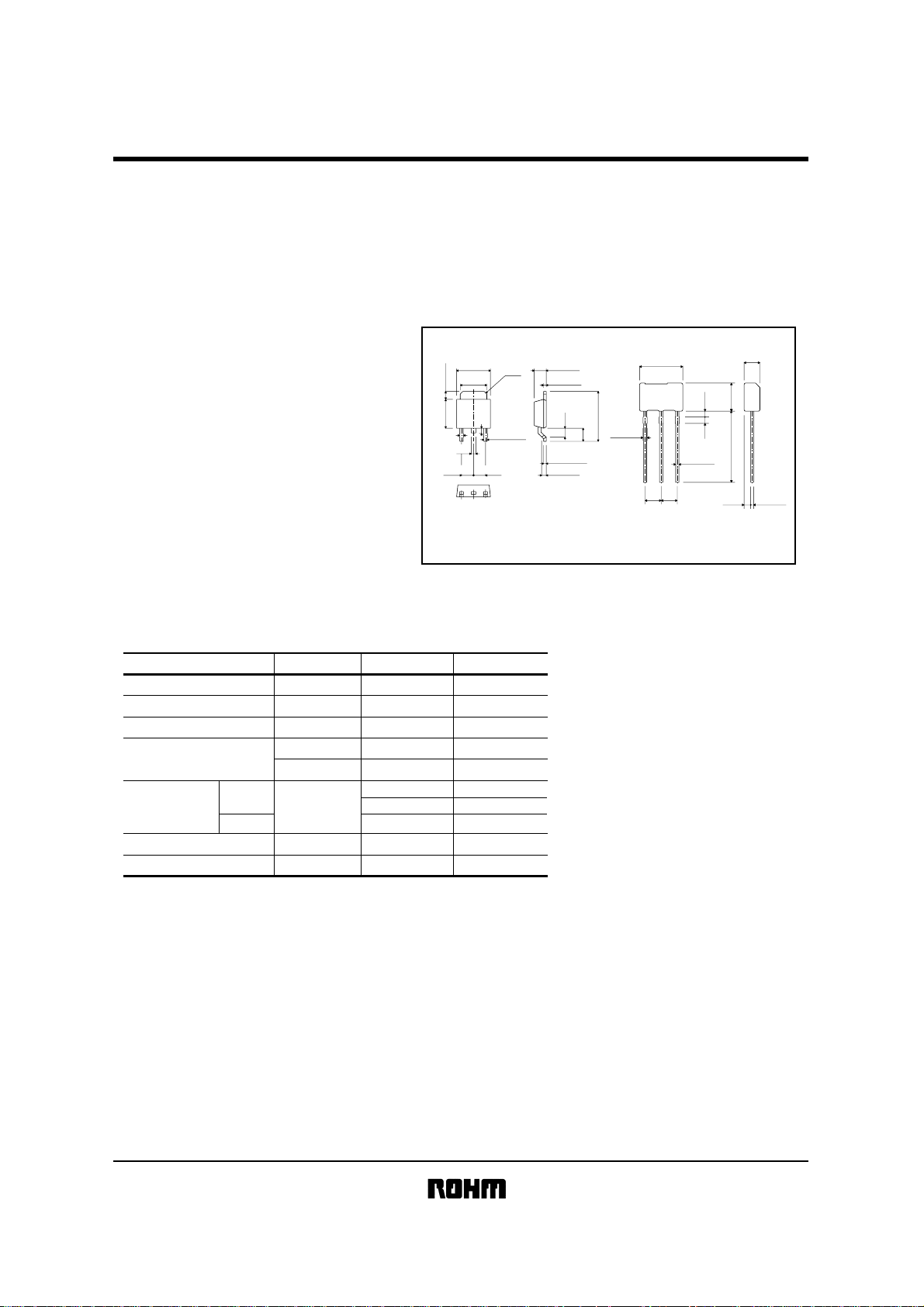
External dimensions
(Units : mm)
2SB1184 2SB1243
6.5±0.2
+0.2
5.1
−0.1
1.5±0.3
−0.1
+0.3
5.5
0.75
0.9
(2)
(1)
ROHM : CPT3
EIAJ : SC-63
0.9
0.65±0.1
2.3±0.22.3±0.2
(3)
C0.5
(1) Base
(2) Collector
(3) Emitter
2.3
−0.1
0.5±0.1
1.5
0.55±0.1
1.0±0.2
9.5±0.5
0.65Max.
2.5
(1)
+0.2
V
V
A (DC)
A (Pulse)−4.5
1
*
W
W (Tc = 25˚C)
2
*
W
°C
°C
6.8±0.2
(2)
(3)
2.54
2.54
ROHM :
0.5
ATV
2.5
±
0.2
0.2
±
0.9
4.4
1.0
0.5
±
±
0.1
14.5
1.05
0.45
±
0.1
(1) Emitter
(2) Collector
(3) Base

Transistors
Electrical characteristics
!!!!
Parameter Symbol
Collector-base breakdown voltage
Collector-emitter breakdown voltage
Emitter-base breakdown voltage
Collector cutoff current
Emitter cutoff current
Collector-emitter saturation voltage
Base-emitter saturation voltage
DC current transfer ratio
Transition frequency
Output capacitance
Measured using pulse current.
*
(Ta = 25°C)
BV
BV
BV
V
V
Cob
CBO
CEO
EBO
I
CBO
I
EBO
CE(sat)
BE(sat)
h
FE
f
T
Min.
Typ. Max. Unit Conditions
−60
−50
−5
-
-
-
-
-
-
-
-
-
--
82
-
-
70
-
50
-
-
-
−1
−1
−1
−1.5 I
390
-
-
V
V
V
µA
µA
V
V
-
MHz
pF
C
= −50µA
I
C
= −1mA
I
E
= −50µA
I
CB
V
EB
V
I
C/IB
C/IB
CE
V
V
CE
CB
V
2SB1184 / 2SB1243
= −40V
= −4V
= −2A/−0.2A
= −2A/−0.2A
= −3V, IC = −0.5A
= −5V, IE = 0.5A, f = 30MHz
= −10V, IE = 0A, f = 1MHz
*
*
*
Packaging specifications and h
!!!!
Package
Code
h
FE
Type
2SB1184
2SB1243
Basic ordering unit (pieces)
PQR
PQR
hFE values are classified as follows :
Item P Q R
FE
h
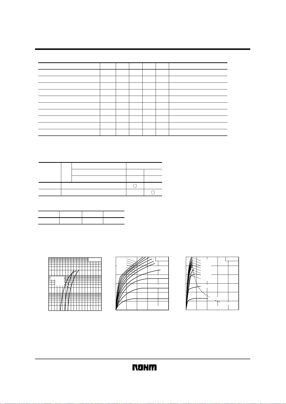
Electrical characteristic curves
!!!!
-10
-5
(A)
C
-2
-1
-0.5
-0.2
-0.1
-0.05
COLLECTOR CURRENT : I
-0.02
-0.01
0 -0.2 -1.4-0.4 -0.8 -1.2 -1.6 -1.8-1.0-0.6
Fig.1 Grounded emitter
82~180 120~270 180~390
VCE = -3V
Ta = 100°C
25°C
-25°C
BASE TO EMITTER VOLTAGE : V
propagation characteristics
BE
(V)
FE
TL TV2
2500 2500
-
-3.0
-50mA
-45mA
-40mA
-35mA
-2.5
(A)
-30mA
C
-25mA
-2.0
-1.5
-1.0
-0.5
COLLECTOR CURRENT : I
0
-10 -2-3-4-5
COLLECTOR TO EMITTER VOLTAGE : V
Fig.2 Grounded emitter output
characteristics ( Ι )
Taping
-
Tc = 25°C
-20mA
-15mA
-10mA
I
B
=
-5mA
0mA
-3.0
-2.5
(A)
C
-2.0
-1.5
-1.0
-0.5
COLLECTOR CURRENT : I
CE
(V)
-50mA
-45mA
-40mA
-35mA
-30mA
-25mA
-20mA
-15mA
-10mA
IB = -5mA
0
-100 -20 -30 -40 -50
COLLECTOR TO EMITTER VOLTAGE : VCE (V)
Tc = 25°C
PC = 15W
IB = 0mA
Fig.3 Grounded emitter output
characteristics ( ΙΙ )
 Loading...