

Rohde&Schwarz R&S®WinIQSIM2™ Digital Standardss User Manual

R&S®SMW-K42/-K83
3GPP FDD incl. enhanced MS/BS
tests, HSPA, HSPA+
User Manual
(;ÙÐè2)
1175669002
Version 22

This document describes the following software options:
●
R&S®SMW-K42 3GPP FDD (1413.3784.xx)
●
R&S®SMW-K83 3GPP HSPA/HSPA+ and enhanced BS/MS tests (1413.4580.xx)
This manual describes firmware version FW 5.00.166.xx and later of the R&S®SMW200A.
© 2022 Rohde & Schwarz GmbH & Co. KG
Muehldorfstr. 15, 81671 Muenchen, Germany
Phone: +49 89 41 29 - 0
Email: info@rohde-schwarz.com
Internet: www.rohde-schwarz.com
Subject to change – data without tolerance limits is not binding.
R&S® is a registered trademark of Rohde & Schwarz GmbH & Co. KG.
Trade names are trademarks of the owners.
1175.6690.02 | Version 22 | R&S®SMW-K42/-K83
The following abbreviations are used throughout this manual: R&S®SMW200A is abbreviated as R&S SMW, R&S®WinIQSIM2TM is
abbreviated as R&S WinIQSIM2; the license types 02/03/07/11/13/16/12 are abbreviated as xx.

R&S®SMW-K42/-K83
Contents
1 Welcome to the 3GPP FDD options....................................................11
1.1 Accessing the 3GPP FDD dialog............................................................................... 13
1.2 What's new...................................................................................................................13
1.3 Documentation overview............................................................................................13
1.3.1 Getting started manual..................................................................................................13
1.3.2 User manuals and help................................................................................................. 14
1.3.3 Tutorials.........................................................................................................................14
1.3.4 Service manual............................................................................................................. 14
1.3.5 Instrument security procedures.....................................................................................14
1.3.6 Printed safety instructions............................................................................................. 14
1.3.7 Data sheets and brochures........................................................................................... 15
Contents
1.3.8 Release notes and open source acknowledgment (OSA)............................................ 15
1.3.9 Application notes, application cards, white papers, etc.................................................15
1.4 Scope........................................................................................................................... 15
1.5 Notes on screenshots.................................................................................................16
2 About the 3GPP FDD options............................................................. 17
2.1 Required options.........................................................................................................17
2.2 Major 3GPP parameters overview............................................................................. 17
2.3 Modulation system 3GPP FDD...................................................................................18
2.3.1 Scrambling code generator........................................................................................... 19
2.3.2 Scrambling unit............................................................................................................. 22
2.3.3 Channelization code generator..................................................................................... 23
2.3.4 Data source...................................................................................................................23
2.3.5 Slot and frame builder................................................................................................... 23
2.3.6 Timing offset..................................................................................................................24
2.3.7 Demultiplexer................................................................................................................ 25
2.3.8 Power control................................................................................................................ 25
2.3.9 Summation and filtering................................................................................................ 26
2.3.10 Multicode.......................................................................................................................26
2.3.11 Orthogonal channel noise (OCNS)............................................................................... 27
2.3.12 HARQ feedback............................................................................................................ 30
3User Manual 1175.6690.02 ─ 22

R&S®SMW-K42/-K83
2.3.13 HS-SCCH less operation.............................................................................................. 32
2.3.14 Higher order modulation................................................................................................33
2.3.15 MIMO in HSPA+............................................................................................................ 35
2.3.16 Dual cell HSDPA (DC-HSDPA)..................................................................................... 40
2.3.17 HS-DPCCH extension for 4C-HSDPA and 8C-HSDPA.................................................44
2.3.18 Dual cell HSUPA (Dual cell E-DCH)..............................................................................44
2.3.19 UE capabilities.............................................................................................................. 44
2.3.20 Uplink discontinuous transmission (UL DTX)................................................................45
2.3.21 Uplink user scheduling.................................................................................................. 47
2.4 Routing and enabling an external control signal.....................................................50
3 3GPP FDD configuration and settings............................................... 51
3.1 General settings for 3GPP FDD signals....................................................................52
Contents
3.2 Trigger settings........................................................................................................... 55
3.3 Marker settings............................................................................................................59
3.4 Clock settings..............................................................................................................61
3.5 Local and global connectors settings.......................................................................62
3.6 Basestations and user equipment settings..............................................................63
3.6.1 Common configuration settings.....................................................................................63
3.6.2 General power settings................................................................................................. 66
3.7 Test setups/models..................................................................................................... 69
3.8 Predefined settings - downlink.................................................................................. 72
3.9 Additional user equipment - uplink........................................................................... 74
3.10 Base station settings.................................................................................................. 75
3.10.1 Common settings.......................................................................................................... 76
3.10.2 Orthogonal channel noise (OCNS) settings.................................................................. 78
3.10.3 Channel table................................................................................................................ 79
3.10.4 Channel graph - BS.......................................................................................................85
3.10.5 Code domain graph - BS...............................................................................................86
3.11 Compressed mode......................................................................................................89
3.11.1 Compressed mode general settings............................................................................. 90
3.11.2 Compressed mode configuration graph........................................................................ 92
3.12 HSDPA settings - BS................................................................................................... 95
3.12.1 Enhanced HSDPA mode settings..................................................................................95
4User Manual 1175.6690.02 ─ 22

R&S®SMW-K42/-K83
3.12.2 MIMO configuration.......................................................................................................97
3.13 HSDPA H-Set mode settings - BS.............................................................................. 99
3.13.1 HSDPA H-Set general settings......................................................................................99
3.13.2 H-Set configuration common settings......................................................................... 100
3.13.3 MIMO settings............................................................................................................. 103
3.13.4 Global settings............................................................................................................ 104
3.13.5 Coding configuration................................................................................................... 107
3.13.6 Signal structure............................................................................................................110
3.13.7 HARQ simulation.........................................................................................................112
3.13.8 Error insertion..............................................................................................................113
3.13.9 Randomly varying modulation and number of codes (Type 3i) settings......................114
3.14 Enhanced settings for P-CPICH - BS1.....................................................................117
3.15 Enhanced settings for P-CCPCH - BS1................................................................... 118
Contents
3.15.1 Channel number and state.......................................................................................... 118
3.15.2 Channel coding - enhanced P-CCPCH BS1............................................................... 119
3.16 Enhanced settings for DPCHs - BS1....................................................................... 120
3.16.1 Channel number and state..........................................................................................121
3.16.2 Channel coding........................................................................................................... 122
3.16.3 Transport channel - enhanced DPCHs BS1................................................................125
3.16.4 Error insertion - enhanced DPCHs BS1......................................................................128
3.16.5 Dynamic power control - enhanced DPCHs BS1........................................................130
3.17 S-CCPCH settings - BS channel table.....................................................................135
3.18 Config AICH/AP-AICH - BS channel table...............................................................137
3.19 DPCCH settings - BS channel table........................................................................ 138
3.19.1 Common slot structure (DPCCH)................................................................................138
3.19.2 TPC settings................................................................................................................141
3.19.3 DPCCH power offset...................................................................................................144
3.20 Config E-AGCH - BS channel table......................................................................... 145
3.21 Config E-RGCH/E-HICH - BS channel table............................................................ 147
3.22 Config F-DPCH - BS channel table.......................................................................... 149
3.22.1 Common settings........................................................................................................ 149
3.22.2 TPC settings................................................................................................................150
3.23 Multi channel assistant - BS.................................................................................... 153
5User Manual 1175.6690.02 ─ 22

R&S®SMW-K42/-K83
3.24 User equipment configuration (UE).........................................................................157
3.24.1 General settings.......................................................................................................... 158
3.24.2 Code domain graph - UE............................................................................................ 161
3.24.3 Channel settings......................................................................................................... 161
3.25 UL-DTX/user scheduling - UE.................................................................................. 162
3.26 Dynamic power control - UE.................................................................................... 166
3.27 Scheduling list...........................................................................................................171
3.28 DPCCH settings - UE................................................................................................ 172
3.29 DPDCH settings - UE................................................................................................ 179
3.29.1 DPDCH common settings........................................................................................... 179
3.29.2 Channel table.............................................................................................................. 181
3.30 HS-DPCCH settings - UE.......................................................................................... 183
3.30.1 About HS-DPCCH.......................................................................................................184
Contents
3.30.2 HS-DPCCH common settings..................................................................................... 186
3.30.3 HS-DPCCH scheduling table (Release 8 and later/RT)..............................................190
3.30.4 HS-DPCCH settings for normal operation (up to Release 7)...................................... 199
3.30.5 MIMO settings HS-DPCCH (up to Release 7)............................................................ 201
3.31 E-DPCCH settings - UE.............................................................................................204
3.32 HSUPA FRC settings - UE.........................................................................................206
3.32.1 FRC general settings.................................................................................................. 206
3.32.2 Coding and physical channels settings....................................................................... 208
3.32.3 DTX mode settings......................................................................................................211
3.32.4 HARQ simulation settings........................................................................................... 213
3.32.5 Bit and block error insertion settings........................................................................... 216
3.33 E-DPDCH settings - UE.............................................................................................218
3.33.1 E-DPDCH common settings........................................................................................219
3.33.2 Channel table.............................................................................................................. 220
3.34 E-DCH scheduling - UE.............................................................................................221
3.35 Global enhanced channel settings - UE1................................................................225
3.35.1 Enhanced channels state............................................................................................226
3.35.2 Channel coding........................................................................................................... 226
3.35.3 Transport channel....................................................................................................... 230
3.35.4 Error insertion..............................................................................................................233
6User Manual 1175.6690.02 ─ 22

R&S®SMW-K42/-K83
3.36 PRACH settings - UE................................................................................................ 234
3.36.1 Graphical display.........................................................................................................236
3.36.2 Preamble settings....................................................................................................... 240
3.36.3 Message part settings................................................................................................. 241
3.36.4 Channel coding state.................................................................................................. 243
3.37 PCPCH settings - UE.................................................................................................245
3.37.1 Graphical display.........................................................................................................247
3.37.2 Preamble settings....................................................................................................... 250
3.37.3 Message part settings................................................................................................. 252
3.37.4 Channel coding settings..............................................................................................256
3.38 Filtering, clipping, ARB settings..............................................................................257
3.38.1 Filter settings...............................................................................................................258
3.38.2 Clipping settings..........................................................................................................259
Contents
3.38.3 ARB settings............................................................................................................... 262
4 How to work with the 3GPP FDD option.......................................... 263
4.1 Resolving domain conflicts..................................................................................... 263
4.2 Using the DL-UL timing offset settings...................................................................266
4.3 Configuring UL-DTX transmission and visualizing the scheduling..................... 266
4.4 Configuring and visualizing the uplink user scheduling...................................... 269
4.5 How to configure the HS-DPCCH settings for 4C-HSDPA tests........................... 271
5 Application sheets............................................................................. 273
5.1 Uplink dual cell HSDPA test signal generation...................................................... 273
5.1.1 Options and equipment required.................................................................................273
5.1.2 Test setup....................................................................................................................273
5.1.3 Generating an uplink DC-HSDPA test signal (non-MIMO mode)................................ 274
5.1.4 Generating an uplink test signal for simultaneous dual cell and MIMO operation...... 276
6 Performing base stations tests according to TS 25.141................ 277
6.1 Introduction............................................................................................................... 277
6.1.1 General considerations............................................................................................... 279
6.1.2 General settings.......................................................................................................... 281
6.1.3 Base station configuration...........................................................................................285
6.1.4 Apply........................................................................................................................... 286
7User Manual 1175.6690.02 ─ 22

R&S®SMW-K42/-K83
6.2 Receiver tests............................................................................................................286
6.2.1 Overview..................................................................................................................... 286
6.2.2 Receiver characteristics.............................................................................................. 290
6.2.3 Performance requirements..........................................................................................311
6.3 Transmitter tests....................................................................................................... 336
6.3.1 Basic configuration......................................................................................................336
6.3.2 Test case 6.4.2 - power control steps..........................................................................336
6.3.3 Test case 6.6 - transmit intermodulation..................................................................... 343
7 Remote-control commands...............................................................348
7.1 General commands...................................................................................................349
7.2 Filter/clipping settings..............................................................................................355
7.3 Trigger settings......................................................................................................... 360
Contents
7.4 Marker settings..........................................................................................................364
7.5 Clock settings............................................................................................................366
7.6 Test models and predefined settings...................................................................... 367
7.7 Setting base stations................................................................................................ 371
7.8 Enhanced channels of base station 1..................................................................... 418
7.8.1 General settings.......................................................................................................... 419
7.8.2 Channel coding........................................................................................................... 420
7.8.3 Dynamic power control settings.................................................................................. 432
7.8.4 Error insertion..............................................................................................................436
7.9 User equipment settings.......................................................................................... 439
7.9.1 General settings.......................................................................................................... 440
7.9.2 Compressed mode settings........................................................................................ 445
7.9.3 DPCCH settings.......................................................................................................... 447
7.9.4 HS-DPCCH settings....................................................................................................454
7.9.5 DPDCH settings.......................................................................................................... 473
7.9.6 PCPCH settings.......................................................................................................... 477
7.9.7 PRACH settings.......................................................................................................... 488
7.9.8 HSUPA settings...........................................................................................................497
7.9.9 UL-DTX and uplink scheduling settings...................................................................... 517
7.9.10 Dynamic power control settings.................................................................................. 522
7.10 Enhanced channels of the user equipment............................................................526
8User Manual 1175.6690.02 ─ 22

R&S®SMW-K42/-K83
7.11 Setting up test cases according to TS 25.141........................................................539
Annex.................................................................................................. 562
A Reference............................................................................................562
List of commands.............................................................................. 569
Index....................................................................................................580
Contents
9User Manual 1175.6690.02 ─ 22

R&S®SMW-K42/-K83
Contents
10User Manual 1175.6690.02 ─ 22

R&S®SMW-K42/-K83
1 Welcome to the 3GPP FDD options
The R&S SMW-K42/-K83 are firmware applications that add functionality to generate
signals in accordance with the WCDMA standard 3GPP FDD.
WCDMA (Wideband CDMA) describes a group of mobile radiocommunication technologies, the details of which differ greatly. The R&S SMW supports the 3GPP FDD stan-
dard developed by the 3GPP (3rd Generation Partnership Project) standardization committee.
The R&S SMW generates the 3GPP FDD signals in a combination of realtime mode
(enhanced channels) and arbitrary waveform mode. Channel coding and simulation of
bit and block errors can be activated for the enhanced channels of Release 99 and for
H-Sets 1 to 5 generated in real time. Channel coding can also be activated for HSDPA/
HSPA+ H-Sets and all HSUPA/HSPA+ FRC channels which are generated in arbitrary
wave mode. Data lists can also be used for the data and TPC fields. The enhanced
state of realtime channels can be switched off to generate specific test scenarios. In
arbitrary waveform mode, the signal is first calculated and then output.
Welcome to the 3GPP FDD options
The R&S SMW simulates 3GPP FDD at the physical channel level and also at the
transport layer level for all channels for which channel coding can be activated.
3GPP FDD/HSDPA/HSUPA/HSPA+ key features
●
Support of all physical channels of 3GPP FDD, HSDPA, HSUPA and HSPA+
●
HSDPA H-Sets 1 to 12 with channel coding; user-definable H-Set configuration
●
HSUPA fixed reference channels with channel coding and HARQ feedback simulation
●
Realtime generation of P-CCPCH and up to three DPCHs in downlink
●
One UE in real time in uplink, up to 128 additional mobile stations via ARB
●
Dynamic power control of a code channel possible
●
Support of UL-DTX, DC-HSDPA, 4C-HSDPA and 8C-HSDPA
Functional overview of option R&S SMW-K42
The following list gives an overview of the functions provided by the option R&S SMWK42 for generating a 3GPP FDD signal:
●
Configuration of up to four base stations and four user equipment.
●
Combination of realtime mode (enhanced channels) and arbitrary waveform mode
●
All special channels and up to 512 channels on the downlink, except HSDPA,
HSUPA and HSPA+
●
Various test models and pre-defined settings for the uplink and the downlink
●
Modulation 16QAM and 64QAM (downlink) for configuring high-speed channels in
continuous mode (test model 5&6, HSDPA)
●
Clipping for reducing the crest factor
●
Misuse TPC" parameter for varying the original normal transmit power over time
●
Simulation of up to 128 additional user equipment
11User Manual 1175.6690.02 ─ 22

R&S®SMW-K42/-K83
The following functions are provided specifically for the receiver test:
●
●
●
●
●
●
Functional overview of the extension R&S SMW-K83
Enhanced MS/BS tests incl. HSDPA extends the 3GPP FDD signal generation with
simulation of high-speed channels in the downlink (HS-SCCH, HS-PDSCH) and the
uplink (HS-DPCCH) and with dynamic power control. HSDPA (high speed downlink
packet access) mode enhances the 3GPP FDD standard by data channels with high
data rates especially for multi-media applications.
Welcome to the 3GPP FDD options
Realtime generation of up to four code channels with the option of using data lists
for the data and TPC fields
Channel coding of the reference measurement channels, AMR and BCH in real
time
Feeding through of bit errors (to test a BER tester) and block errors (to test a BLER
tester)
Simulation of orthogonal channel noise (OCNS in accordance with TS 25.101)
Presettings in accordance with 3GPP specifications
HSDPA Downlink in continuous mode (test model 5&6 for TX tests)
The following functions are provided for enhanced BS/MS tests including HSDPA:
●
HSDPA uplink
●
HSDPA downlink (packet mode and H-Set mode without CPC, 64QAM and MIMO)
●
Dynamic Power Control
●
Predefined and user-definable H-Sets
●
Assistance in the setting of the appropriate sequence length for arbitrary waveform
mode
HSUPA extends the 3GPP FDD signal generation with full HSUPA (high speed uplink
packet access) support. Option K59 3GPP FDD HSPA+ extends the HSDPA and/or
HSUPA signal generation with HSPA+ features in the downlink and uplink
The following functions are provided for HSUPA:
●
HSUPA Downlink (RX measurements on 3GPP FDD UEs with correct timing )
●
HSUPA Uplink (RX measurements on 3GPP FDD node BS supporting HSUPA)
●
HSUPA HARQ Feedback support
The following functions are provided for HSPA+:
●
Downlink 64QAM with channel coding
●
Uplink 16QAM (4PAM)
●
Downlink MIMO
●
Uplink ACK/PCI/CQI feedback for downlink MIMO and/or Dual-Cell HSDPA
●
CPC in downlink (HS-SCCH less operation, enhanced F-DPCH) and uplink (ULDTX, Uplink DPCCH slot format 4)
●
Support for the generation of 3i OCNS and for randomly varying modulation and
the number of HS-PDSCH channels in H-Set over time (type 3i enhanced performance requirements tests).
12User Manual 1175.6690.02 ─ 22

R&S®SMW-K42/-K83
This user manual contains a description of the functionality that the application provides, including remote control operation.
All functions not discussed in this manual are the same as in the base unit and are
described in the R&S SMW user manual. The latest version is available at:
www.rohde-schwarz.com/manual/SMW200A
Installation
You can find detailed installation instructions in the delivery of the option or in the
R&S SMW service manual.
1.1 Accessing the 3GPP FDD dialog
To open the dialog with 3GPP FDD settings
► In the block diagram of the R&S SMW, select "Baseband > 3GPP FDD".
Welcome to the 3GPP FDD options
Documentation overview
A dialog box opens that display the provided general settings.
The signal generation is not started immediately. To start signal generation with the
default settings, select "State > On".
1.2 What's new
This manual describes firmware version FW 5.00.166.xx and later of the
R&S®SMW200A.
Compared to the previous version some power reference settings require option
R&S SMW-K83, see "Power Reference" on page 67.
1.3 Documentation overview
This section provides an overview of the R&S SMW user documentation. Unless specified otherwise, you find the documents on the R&S SMW product page at:
www.rohde-schwarz.com/manual/smw200a
1.3.1 Getting started manual
Introduces the R&S SMW and describes how to set up and start working with the product. Includes basic operations, typical measurement examples, and general information, e.g. safety instructions, etc. A printed version is delivered with the instrument.
13User Manual 1175.6690.02 ─ 22

R&S®SMW-K42/-K83
1.3.2 User manuals and help
Separate manuals for the base unit and the software options are provided for download:
●
●
The contents of the user manuals are available as help in the R&S SMW. The help
offers quick, context-sensitive access to the complete information for the base unit and
the software options.
All user manuals are also available for download or for immediate display on the Internet.
Welcome to the 3GPP FDD options
Documentation overview
Base unit manual
Contains the description of all instrument modes and functions. It also provides an
introduction to remote control, a complete description of the remote control commands with programming examples, and information on maintenance, instrument
interfaces and error messages. Includes the contents of the getting started manual.
Software option manual
Contains the description of the specific functions of an option. Basic information on
operating the R&S SMW is not included.
1.3.3 Tutorials
The R&S SMW provides interactive examples and demonstrations on operating the
instrument in form of tutorials. A set of tutorials is available directly on the instrument.
1.3.4 Service manual
Describes the performance test for checking compliance with rated specifications, firmware update, troubleshooting, adjustments, installing options and maintenance.
The service manual is available for registered users on the global Rohde & Schwarz
information system (GLORIS):
https://gloris.rohde-schwarz.com
1.3.5 Instrument security procedures
Deals with security issues when working with the R&S SMW in secure areas. It is available for download on the Internet.
1.3.6 Printed safety instructions
Provides safety information in many languages. The printed document is delivered with
the product.
14User Manual 1175.6690.02 ─ 22

R&S®SMW-K42/-K83
1.3.7 Data sheets and brochures
The data sheet contains the technical specifications of the R&S SMW. It also lists the
options and their order numbers and optional accessories.
The brochure provides an overview of the instrument and deals with the specific characteristics.
See www.rohde-schwarz.com/brochure-datasheet/smw200a
1.3.8 Release notes and open source acknowledgment (OSA)
The release notes list new features, improvements and known issues of the current
firmware version, and describe the firmware installation.
The open-source acknowledgment document provides verbatim license texts of the
used open source software.
See www.rohde-schwarz.com/firmware/smw200a
Welcome to the 3GPP FDD options
Scope
1.3.9 Application notes, application cards, white papers, etc.
These documents deal with special applications or background information on particular topics.
See www.rohde-schwarz.com/application/smw200a and www.rohde-schwarz.com/
manual/smw200a
1.4 Scope
Tasks (in manual or remote operation) that are also performed in the base unit in the
same way are not described here.
In particular, it includes:
●
Managing settings and data lists, like saving and loading settings, creating and
accessing data lists, or accessing files in a particular directory.
●
Information on regular trigger, marker and clock signals and filter settings, if appropriate.
●
General instrument configuration, such as checking the system configuration, configuring networks and remote operation
●
Using the common status registers
For a description of such tasks, see the R&S SMW user manual.
15User Manual 1175.6690.02 ─ 22

R&S®SMW-K42/-K83
1.5 Notes on screenshots
When describing the functions of the product, we use sample screenshots. These
screenshots are meant to illustrate as many as possible of the provided functions and
possible interdependencies between parameters. The shown values may not represent
realistic usage scenarios.
The screenshots usually show a fully equipped product, that is: with all options installed. Thus, some functions shown in the screenshots may not be available in your particular product configuration.
Welcome to the 3GPP FDD options
Notes on screenshots
16User Manual 1175.6690.02 ─ 22

R&S®SMW-K42/-K83
2 About the 3GPP FDD options
Some background knowledge on basic terms and principles used in the 3GPP FDD
modulation system is provided here for better understanding of the required configuration settings.
2.1 Required options
The basic equipment layout for generating 3GPP FDD signals includes the:
●
●
●
●
About the 3GPP FDD options
Major 3GPP parameters overview
Standard or wideband Baseband Generator (R&S SMW-B10/-B9)
Baseband Main Module (R&S SMW-B13) or Wideband baseband main module
(R&S SMW-B13XT)
Frequency option (e.g. R&S SMW-B1003)
Digital standard 3GPP FDD (R&S SMW-K42)
The following options are required to support all 3GPP-related settings described in
this user manual:
●
Standard or wideband Baseband Generator (R&S SMW-B10/-B9)
●
Baseband Main Module, two I/Q paths (R&S SMW-B13T) or Wideband baseband
main module (R&S SMW-B13XT)
●
Frequency option (e.g. R&S SMW-B1003)
●
Frequency option (e.g. R&S SMW-B2003)
●
Option digital standard 3GPP FDD (R&S SMW-K42)
●
Option 3GPP FDD HSPA/HSPA+, Enhanced BS/MS Tests (R&S SMW-K83)
●
Further options are required to perform all test cases implemented in the "Test
Case Wizard".
For more information, see data sheet.
2.2 Major 3GPP parameters overview
Table 2-1 gives an overview of parameters of the modulation system 3GPP FDD.
17User Manual 1175.6690.02 ─ 22

R&S®SMW-K42/-K83
Table 2-1: Parameters of the modulation system
Parameter Value
Chip rate 3.84 Mcps
About the 3GPP FDD options
Modulation system 3GPP FDD
Channel types
Symbol rates 7.5 ksps, 15 ksps, 30 ksps to 960 ksps depending on the channel type (down-
Downlink:
●
Primary Common Pilot Channel (P-CPICH)
●
Secondary Common Pilot Channel (S-CPICH)
●
Primary Sync Channel (P-SCH)
●
Secondary Sync Channel (S-SCH)
●
Primary Common Control Phys. Channel (P-CCPCH)
●
Secondary Common Control Phys. Channel (S-CCPCH)
●
Page Indication Channel (PICH)
●
Acquisition Indication Channel (AICH)
●
Access Preamble Acquisition Indication Channel (AP-AICH)
●
Collision Detection Acquisition Indication Channel (CD-AICH)
●
Phys. Downlink Shared Channel (PDSCH)
●
Dedicated Physical Control Channel (DL-DPCCH)
●
Dedicated Phys. Channel (DPCH)
●
High-Speed Shared Control Channel (HS-SCCH)
●
High-Speed Physical Downlink Shared Channel (HS-PDSCH), Modulation
QPSK, 16 QAM or 64QAM
●
HSUPA channels (E-AGCH, E-RGCH, E-HICH, F-DPCH)
Uplink:
●
Phys. Random Access Channel (PRACH)
●
Phys. Common Packet Channel (PCPCH)
●
Dedicated Physical Control Channel (DPCCH)
●
Dedicated Physical Data Channel (DPDCH)
●
High Speed Dedicated Physical Control Channel (HS-DPCCH)
●
E-DCH Dedicated Physical Control Channel (E-DPCCH)
●
E-DCH dedicated physical data channel (E-DPDCH)
link)
15 ksps, 30 ksps, 60 ksps to 1920 ksps depending on the channel type (uplink)
Channel count In downlink 4 base stations each with up to 128 DPCHs and 11 special channels.
In uplink 4 user equipment either with PRACH or PCPCH or a combination of
DPCCH, up to 6 DPDCH, HS-DPCCH, E-DPCCH and up to 4 E-DPDCH channels.
Frame structure Timeslot: 0.667 ms,
Subframe: 3 timeslots = 2 ms
Radio frame: 15 timeslots = 10 ms
The frame structure in symbols depends on the symbol rate.
Scrambling code Downlink: 18-bit M sequence
Uplink: 25-bit M sequence in long mode and 8-bit M sequence in short mode
Channelization code for
most of the channel
types
"Orthogonal Variable Spreading Factor Code (OVSF)" square matrix of dimension chip rate/symbol rate
2.3 Modulation system 3GPP FDD
The following block diagram shows the components of the 3GPP FDD transmission
system.
18User Manual 1175.6690.02 ─ 22
R&S®SMW-K42/-K83
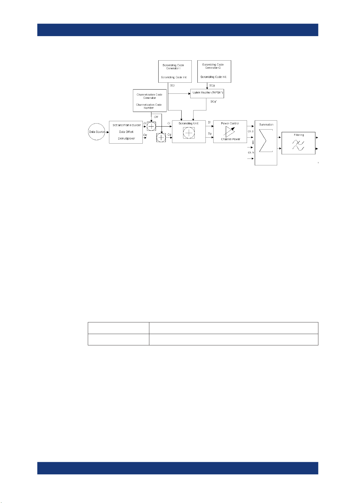
Figure 2-1: Components of the 3GPP FDD transmission system
2.3.1 Scrambling code generator
About the 3GPP FDD options
Modulation system 3GPP FDD
The scrambling code generator (previously called long code generator) is used to
scramble the chip sequence as a function of the transmitter.
Depending on the link direction and mode (long or short), the structure and initialization
regulation of the generator are different.
2.3.1.1 Downlink scrambling code generator
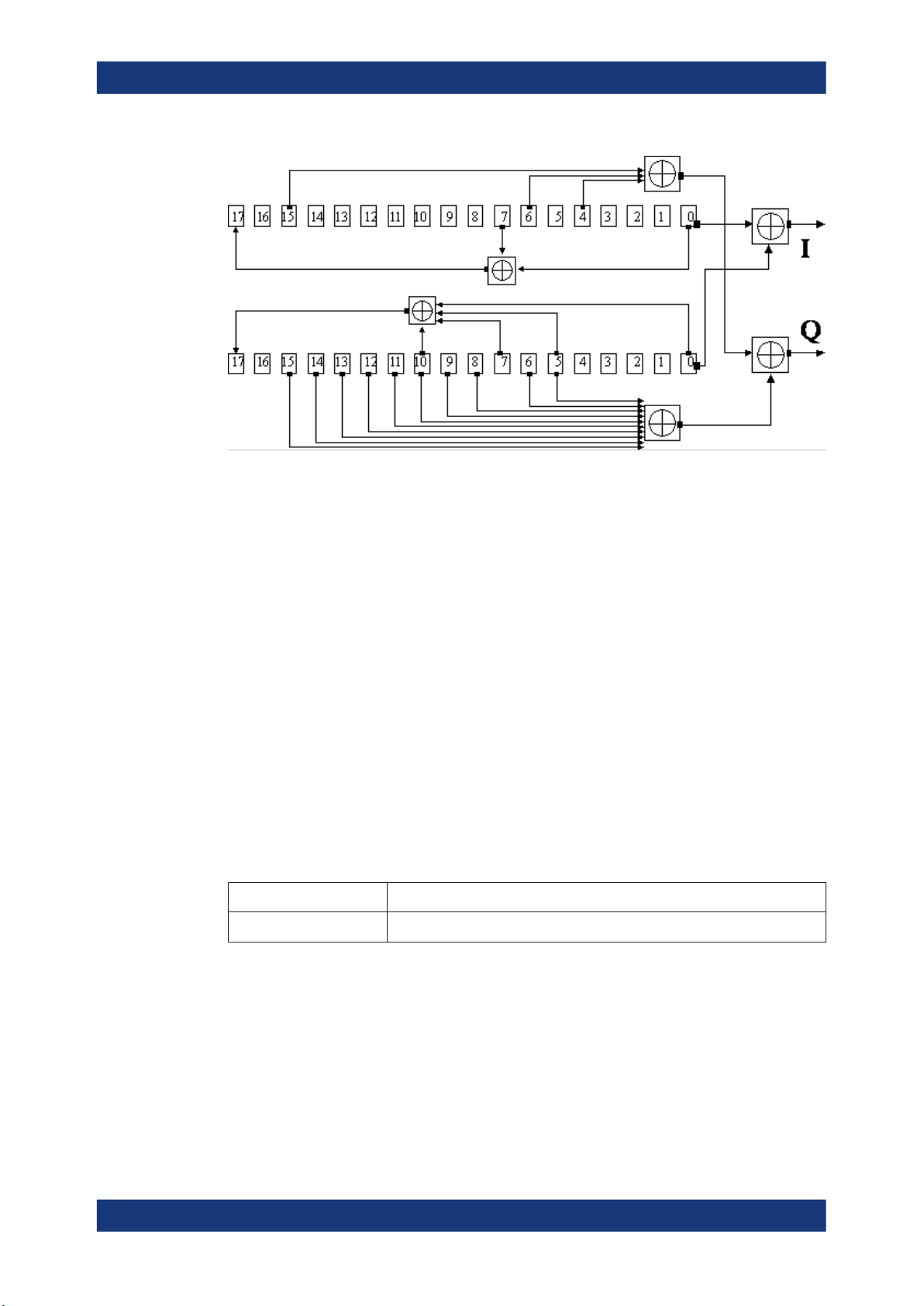
This generator consists of a pair of shift registers from which the binary sequences for
in-phase and orthogonal component of the scrambling code are determined. The Fig-
ure 2-2 shows that the I component is produced as EXOR operation of the LSB out-
puts. However the register contents are first masked and read out for the Q component
and then EXORed.
Table 2-2: Generator polynomials of the downlink scrambling code generators
Shift register 1
Shift register 2
x18+x7+1
x18+x10+x7+x5+1
19User Manual 1175.6690.02 ─ 22
R&S®SMW-K42/-K83
Figure 2-2: Structure of downlink scrambling code generator
The shift registers are initialized by loading shift register 1 with "0...01" and shift register 2 completely with "1". In addition, shift register 1 is wound forward by n cycles, n
being the scrambling code number or scrambling code (SC) for short.
About the 3GPP FDD options
Modulation system 3GPP FDD
After a cycle time of one radio frame the generators are reset, i.e. the above initialization is carried out again.
2.3.1.2 Uplink scrambling code generator
In the uplink, a differentiation is made between two SC modes. The long SC can be
used for all types of channel. The short SC can be used as an alternative to the long
SC for all channels except PRACH and PCPCH.
Uplink long scrambling code
Principally, the code generator of the long SC in the uplink is of the same structure as
the SC in the downlink. However, the generator polynomials of the shift registers and
the type of initialization are different.
Table 2-3: Generator polynomials of the uplink long scrambling code generator
Shift register 1
Shift register 2
x25+x3+1
x25+x3+x2+x+1
The shift registers are initialized by allocating 1 to shift register 1-bit number 24 and the
binary form of the scrambling code number n to bits 23 to 0. Shift register 2 is loaded
with "1".
The read-out positions for the Q component are defined such that they correspond to
an IQ offset of 16.777.232 cycles.
After a cycle time of one radio frame the generators are reset, i.e. the above initialization is carried out again.
20User Manual 1175.6690.02 ─ 22
R&S®SMW-K42/-K83
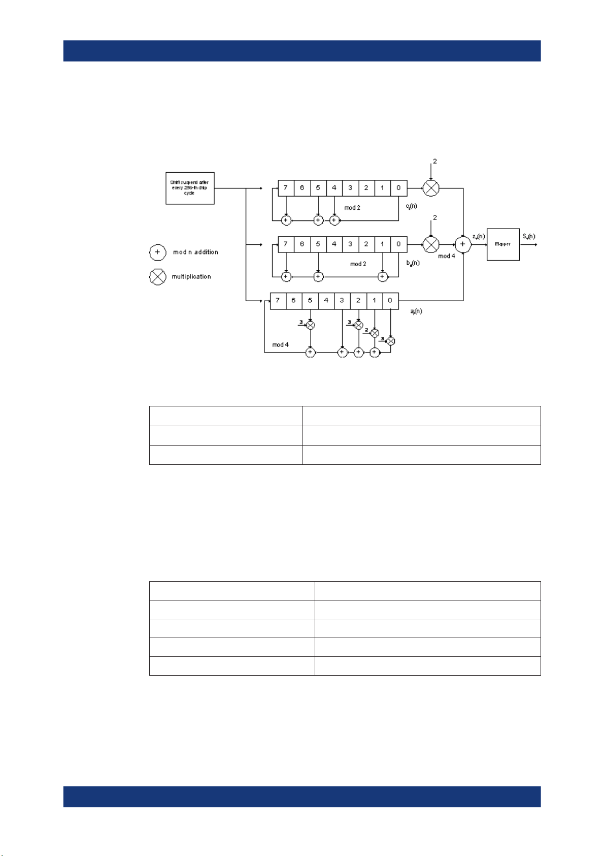
Uplink short scrambling code
The code generator of the short SC in the uplink consists of a total of three coupled
shift registers.
About the 3GPP FDD options
Modulation system 3GPP FDD
Figure 2-3: Structure of uplink short scrambling code generator
Table 2-4: Generator polynomials of uplink short scrambling code generator
Shift register 1 (binary)
Shift register 2 (binary)
Shift register 3 (quaternary)
x8+x7+x5+x4+1
x8+x7+x5+x+1
x8+x5+3x3+x2+2x+1
The output sequences of the two binary shift registers are weighted with factor 2 and
added to the output sequence of the quaternary shift register. The resulting quaternary
output sequence is mapped into the binary complex level by the mapper block.
For initialization, of the three 8-bit shift registers (in a modified way) the binary form of
the 24-bit short SC number n is used. For details see 3GPP TS 25 213, "Spreading
and Modulation".
Table 2-5: Mapping of the quaternary output sequence into the binary IQ level
zv(n) Sv(n)
0 +1 + j1
1 -1 + j1
2 -1 - j1
3 +1 - j1
Preamble scrambling code generator
When generating the preambles of the PRACH and PCPCH, a special SC is used. It is
based on the Long SC described under a), however only the I component is taken and
subsequently a pointer (e
j(PI/4 + PI/4 * k)
, k=0 to 4095) modulated upon it.
21User Manual 1175.6690.02 ─ 22
R&S®SMW-K42/-K83
Modification of the long and short scrambling code output sequence
The scrambling code sequence of the Q component is modified as standard to reduce
the crest factor of the signal. Zero-crossings can thus be avoided for every second
cycle. (This method is often called "HPSK").
For details see 3GPP TS 25 213, "Spreading and Modulation". The R&S SMW uses a
decimation factor of 2.
2.3.2 Scrambling unit
In the scrambling unit, the output of the scrambling code generator is linked with
spread symbols.
The input signal and the scrambling code signal are interpreted as complex signal:
(Ci , Cq , SCi , SCq' ∈ { -1, +1 })
The output signal is a complex multiplication of two signals:
Si + j Sq = (Ci + j Cq) * (SCi + j SCq')
About the 3GPP FDD options
Modulation system 3GPP FDD
The following equations apply:
Si = CiSCi – CqSCq'
Sq = CiSCq' + CqSC
i
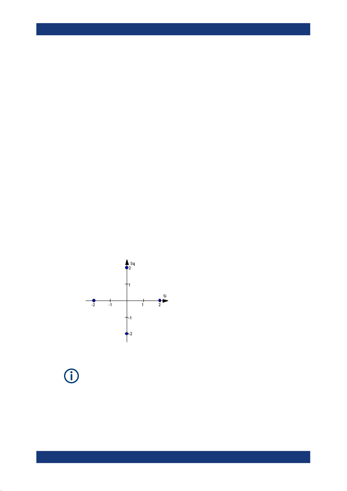
The signal thus obtained can be interpreted as a QPSK signal with the following constellation diagram:
Figure 2-4: Constellation diagram of a channel with 0 dB power
There are auxiliary conditions for some types of channels that can result in different
constellation diagrams. If, for instance, symbols of the SCH are coded, a BPSK constellation is obtained without the scrambling unit.
Furthermore, with HSDPA and HSPA+, the higher order modulations 4PAM, 16QAM
and 64QAM were introduced.
22User Manual 1175.6690.02 ─ 22

R&S®SMW-K42/-K83
2.3.3 Channelization code generator
The channelization code generator cyclically outputs a channel-specific bit pattern. The
length of the cycle corresponds to the period of the source symbol to be spread, i.e.
the number of bits corresponds to the spread factor. The spreading sequence for the I
and Q branch is identical (real value). Spreading is a simple EXOR operation.
Two different channelization code generators are used depending on the type of channel:
Channelization code generator for all channels except SCH
Due to this channelization code, the channel separation takes place in the sum signal.
The channelization code number is the line of an orthogonal spreading matrix which is
generated according to an iterative scheme ("OVSF").
Channelization code generator SCH
This generator replaces the one described above if the synchronization code symbol of
the SCH channels is spread.
About the 3GPP FDD options
Modulation system 3GPP FDD
The spreading matrix is replaced by a method that forms the spreading sequence. For
details, see 3GPP TS 25 213.
2.3.4 Data source
The data and TPC fields of the enhanced channels (realtime channels) can be filled
from data lists containing user-defined data. This allows user information from the
physical layer or from higher layers such as the transport layer to be introduced into
the signal generation process.
The choice of data sources is crucially important for the signal characteristics. The constellation diagram and the crest factor in particular are modeled to a great extent by a
suitable choice of data.
2.3.5 Slot and frame builder
The bits from the data source are first entered into a frame structure. The frames are
made up of three hierarchical levels:
Table 2-6: Hierarchical structure of 3GPP FDD frames
Hierarchy Length in ms Remarks
Timeslot 0.667
Subframe 2 ms One subframe consists of 3 timeslots.
Radio frame 10 After a radio frame, pilot symbols are repeated. One radio
frame consists of 15 timeslots.
A frame is also the length of a scrambling code cycle. Frames
are the basic unit.
The sequence length is stated in radio frames.
23User Manual 1175.6690.02 ─ 22

R&S®SMW-K42/-K83
The configuration of the timeslots depends on the channel type and symbol rate. The
following components are distinguished:
●
●
●
●
●
●
●
About the 3GPP FDD options
Modulation system 3GPP FDD
Pilot sequence
The pilot sequence characterizes the timeslot position within the radio frame and
also depends on the symbol rate, transmit diversity and the pilot length parameter.
Channel types DPCH, S-CCPCH, DL-DPCCH, DPCCH, PRACH and PCPCH have
a pilot sequence.
Synchronization code symbol
The synchronization code symbol is the only symbol of the SCH.
TPC symbol
This symbol is used to control the transmit power. It is used in DPCH, DL-DPCCH
and DPCCH.
A bit pattern for the sequence of TPC symbols can be indicated as a channel-specific pattern.
Data symbols
These symbols carry the user information and are fed from the data source. They
are used in DPCH, P-CCPCH, S-CCPCH, PDSCH, E-AGCH, E-RGCH, E-HICH,
DPDCH, PRACH, PCPCH, HS-PDSCH and E-DPDCH.
Signature
The signature is used in PRACH and PCPCH. 16 fixed bit patterns are defined.
TFCI (transport format combination indicator)
If enabled, the TFCI is used in DPCH/DPCCH. In this case, a code sequence with
the length of 30 is defined using this value and distributed among 15 subsequent
timeslots. In PRACH and PCPCH, the TFCI field is provided as standard.
FBI
Feedback indication bits are only used in DPCCH and PCPCH.
2.3.6 Timing offset
The symbol stream can be shifted in time relative to the other channels. For this purpose, a timing offset can be entered into the channel table, stating the range of shifting
in multiples of 256 chips. Since the generator does not generate infinite symbol
streams like a real-time system, this offset is implemented as a rotation.
Example:
DPCH 30 ksps, 1 timeslot, timing offset = 2;
2 x 256 chips = 512 chip offset;
4 data symbols shifting at a symbol rate of 30 ksps (1 symbol corresponds to 3.84
Mcps / 30 ksps = 128 chips).
Previously:
11 11 11 11 00 01 10 11 00 10 01 11 11 01 00 01 10 11 01 00
Afterwards:
10 11 01 00 11 11 11 11 00 01 10 11 00 10 01 11 11 01 00 01
24User Manual 1175.6690.02 ─ 22
R&S®SMW-K42/-K83
The use of the timing offset usually causes a reduction of the crest factor of the total
signal. This is based on the fact that the spreading chips CH and scramble chips
SCi/SCq' that are applied to the pilot sequences of the channels are not always the
same.
2.3.7 Demultiplexer
In the downlink, the symbol stream is divided into 2-bit streams Di and Dq before processing in the spreading unit.
For example, if QPSK modulation is used for a channel, the symbol stream is processed as follows:
●
●
For the above example with timing offset:
Di = 1 1 0 0 1 1 1 1 0 0 1 1 0 1 0 1 1 0 0 0
About the 3GPP FDD options
Modulation system 3GPP FDD
It is divided by allocating bits 1, 3, 5, to 2n-1 to the in-phase bitstream D
It is divided by allocating bits 2, 4, 6, 2n to the quadrature bitstream Dq.
i
Dq = 0 1 1 0 1 1 1 1 0 1 0 1 0 0 1 1 1 1 0 1
(left-hand bit is always the first one in the time sequence)
In the uplink, independent data are used for the two paths.
PRACH/PCPCH: Preamble : signature parallel to I and Q
DPCCH/E-DPCCH: all bits to I, Q always unused
DPDCH/HS-DPCCH/EDPDCH:
2.3.8 Power control
After spreading and scrambling, a channel-specific power factor p is applied to the signal. A value of -6 dB therefore results in half the level (or ¼ power) and the following
diagram (DPCH):
Message part : data to I, pilot, TPC and TFCI to Q
all bits are always to I or Q (dependent on channel number), the other
path is unused.
25User Manual 1175.6690.02 ─ 22

R&S®SMW-K42/-K83
Figure 2-5: Constellation diagram of a channel with –6 dB power
2.3.9 Summation and filtering
After application of the channel power, the components of the individual channels are
summed up.
About the 3GPP FDD options
Modulation system 3GPP FDD
The constellation diagram of the sum signal is obtained by superposition of the diagrams of the individual channels. If the signal consists of two channels with power of -6
dB and -12 dB and each channel contains independent source data (DPCH), the following constellation diagram is obtained:
Figure 2-6: Constellation diagram of a 3GPP WCDMA signal with two DPCH channels
2.3.10 Multicode
3GPP FDD supports multicode transmission for downlink-dedicated physical channels
(DPCH).
This form of transmission is used for channels intended for the same receiver, i.e.
those receivers that belong to a radio link. The first channel of this group is used as a
master channel.
Shared parts (pilot, TPC and TCFI) are spread for all channels using the spreading
code of the master channel.
26User Manual 1175.6690.02 ─ 22
R&S®SMW-K42/-K83
Instead of changing the spreading code within a slot several times, the master code
rather than the shared parts can be sent at higher power. Then blank out the other
channels correspondingly.
2.3.11 Orthogonal channel noise (OCNS)
With orthogonal channel noise, a practical downlink signal is generated to test the
maximum input levels of user equipment in accordance with standard specifications.
This simulates the data and control signals of the other orthogonal channels in the
downlink. 3GPP TS 25.101 contains a precise definition of the required appearance of
the OCNS signal.
Four different OCNS scenarios are defined in the standard. One standard scenario,
two scenarios for HSDPA test cases and one scenario for type 3i enhanced performance requirements tests according to 3GPP TS34.121-1.
When activating OCNS and depending on the selected OCNS mode, different channel
groups with different presetting are assigned as in the following tables. These channels
cannot be edited in the channel table.
About the 3GPP FDD options
Modulation system 3GPP FDD
2.3.11.1 Standard, HSDPA and HSDPA2 modes
For the "Standard", "HSDPA" and "HSDPA2" modes, the OCNS channels are all normal DPCHs. The symbol rate is set at 30 ksps and the pilot length to 8 bits.
The powers of the OCNS channel outputs are relative. In the R&S SMW, the power of
the OCNS component is set so that OCNS channels supplement the remaining channels in BS1 to make total power of 0 dB (linear 1).
It is not possible to adapt the OCNS power if the linear power of the remaining channels is >1, this produces an error message. The OCNS channels are then given the
maximum power (all -80 dB).
The "Total Power" display is updated after automatic calculation of the output; it is not
possible to use "Adjust Total Power" to make the setting.
Table 2-7: Defined settings for the OCNS signal in base station 1 in Standard mode
Chan. code Timing offset
(x256Tchip)
2 86 -1 DPCH 30 ksps 8 bit
11 134 -3 DPCH 30 ksps 8 bit
17 52 -3 DPCH 30 ksps 8 bit
23 45 -5 DPCH 30 ksps 8 bit
Level setting
(dB)
Channel type Symbol rate Pilot length
31 143 -2 DPCH 30 ksps 8 bit
38 112 -4 DPCH 30 ksps 8 bit
47 59 -8 DPCH 30 ksps 8 bit
55 23 -7 DPCH 30 ksps 8 bit
27User Manual 1175.6690.02 ─ 22

R&S®SMW-K42/-K83
About the 3GPP FDD options
Modulation system 3GPP FDD
Chan. code Timing offset
(x256Tchip)
62 1 -4 DPCH 30 ksps 8 bit
69 88 -6 DPCH 30 ksps 8 bit
78 30 -5 DPCH 30 ksps 8 bit
85 18 -9 DPCH 30 ksps 8 bit
94 30 -10 DPCH 30 ksps 8 bit
125 61 -8 DPCH 30 ksps 8 bit
113 128 -6 DPCH 30 ksps 8 bit
119 143 0 DPCH 30 ksps 8 bit
Table 2-8: Defined settings for the OCNS signal in base station 1 in HSDPA mode
Channelization
code at SF=128
122 0 DPCH 30 ksps 8 bit
123 -2 DPCH 30 ksps 8 bit
124 -2 DPCH 30 ksps 8 bit
125 -4 DPCH 30 ksps 8 bit
Relative Level
setting (dB)
Level setting
(dB)
Channel type Symbol rate Pilot length
Channel type Symbol rate Pilot length
126 -1 DPCH 30 ksps 8 bit
127 -3 DPCH 30 ksps 8 bit
Table 2-9: Defined settings for the OCNS signal in base station 1 in HSDPA2 mode
Channelization
code at SF=128
4 0 DPCH 30 ksps 8 bit
5 -2 DPCH 30 ksps 8 bit
6 -4 DPCH 30 ksps 8 bit
7 -1 DPCH 30 ksps 8 bit
2.3.11.2 3i OCNS mode
Option: R&S SMW-K83
In the "3i" OCNS mode, 16 DPCH channels are inserted in the BS 1 channel according
to 3GPP TS34.121-1, chapter E.5E.
According to 3GPP TS34.121-1, table E.5E.1.3, the channelization code of each of
these channels changes randomly on a symbol-by-symbol basis between two possible
values.
Relative Level
setting (dB)
Channel type Symbol rate Pilot length
28User Manual 1175.6690.02 ─ 22

R&S®SMW-K42/-K83
The power control sequence modeling according to 3GPP TS34.121-1, chapter E.5E.3
is applied to these channels. The power relationship between these channels is
according to 3GPP TS34.121-1, table E.5E.1.3 only during the first slot. It can deviate
in the subsequent slots up to a certain range, but the total power of these channels is
maintained constant (by normalization).
If the "3i" OCNS mode is activated, the OCNS channels are automatically leveled to
have total power of 0 dB for all channels of BS 1.
About the 3GPP FDD options
Modulation system 3GPP FDD
Table 2-10: Defined settings for the OCNS signal in base station 1 in 3i mode
Slot format Symbol Rate,
kbps
10 30 2 108 -1.7
10 30 3 103 -2.7
10 30 5 109 -3.5
10 30 6 118 -0.8
10 30 90 4 -6.2
10 30 94 123 -4.6
10 30 96 111 -2.3
10 30 98 106 -4.1
10 30 99 100 -3.1
10 30 101 113 -5.1
12 60 52 44 0.0
10 30 110 124 -4.6
First Ch. code of
the channel
Second Ch. code
of the channel
Relative Power,
dB
(before the 0 dB
adjustment)
10 30 114 115 -4.8
10 30 116 126 -4.8
12 60 60 46 -1.1
10 30 125 95 -4.1
29User Manual 1175.6690.02 ─ 22

R&S®SMW-K42/-K83
Refer to Chapter 3.13.9, "Randomly varying modulation and number of codes (Type 3i)
settings", on page 114 for description of the further settings required for the 3i
enhanced performance requirements tests according to 3GPP TS 34.121-1.
2.3.12 HARQ feedback
The HARQ Feedback functionality extends the basic 3GPP FDD option in order to
meet the requirements defined in 3GPP TS 25.141, chapter 8.12 and 8.13.
This allows you to control the transmission of the HSUPA fixed reference channels
(FRC 1-7), the HSPA+ fixed reference channel (FPC 8) and the user defined fixed reference channels dynamically. An ACK from the base station leads to the transmission
of a new packet. In contrast, a NACK forces the instrument to retransmit the packet
with a new channel coding configuration (i.e. new redundancy version RV) of the concerned HARQ process.
2.3.12.1 Limitations
About the 3GPP FDD options
Modulation system 3GPP FDD
Although an arbitrary data source can be selected, the same user data is used for all
HARQ processes and for all retransmissions.
Example:
If FRC4 is configured and the data source is set to PN9, then the first 5076 bits of the
PN9 are used as input for all four HARQ processes. This happens regardless of which
retransmission is performed. Note that the bitstream after channel coding is different
for different retransmissions due to different redundancy versions.
Furthermore, "DTX-Mode" and "Bit-Error-Insertion/Block-Error-Insertion" are not available in this mode.
2.3.12.2 Setup
If an instrument with fading simulation is available, no more test equipment is needed
in order to fulfill the test setup described in 3GPP TS 25.141, annex B.3.4.
As the instrument has no RF input available, the HARQ feedback from the base station
is expected as a TTL signal. The instrument provides two input connectors for this signal, the LEVATT connector on the external AUX I/O BNC adapter board R&S SMx-Z5
and the USER 1 connector on the instrument. Use the parameter Connector (HARQ)
to enable the currently used in each baseband.
A high level (TTL) is interpreted as an ACK, while a low level corresponds to a NACK.
Use the parameter ACK Definition (HARQ) to redefined it.
2.3.12.3 Timing
In general, the ACK/NACK feedback from the base station is available at the selected
instruments connector (LEVATT or the USER 1) with the same timing as the E-HICH is
30User Manual 1175.6690.02 ─ 22
 Loading...